EP1184690B1 - Optical element - Google Patents
Optical element Download PDFInfo
- Publication number
- EP1184690B1 EP1184690B1 EP01120593A EP01120593A EP1184690B1 EP 1184690 B1 EP1184690 B1 EP 1184690B1 EP 01120593 A EP01120593 A EP 01120593A EP 01120593 A EP01120593 A EP 01120593A EP 1184690 B1 EP1184690 B1 EP 1184690B1
- Authority
- EP
- European Patent Office
- Prior art keywords
- photonic crystal
- region
- holes
- optical element
- refractive index
- Prior art date
- Legal status (The legal status is an assumption and is not a legal conclusion. Google has not performed a legal analysis and makes no representation as to the accuracy of the status listed.)
- Expired - Lifetime
Links
Images


Classifications
-
- G—PHYSICS
- G02—OPTICS
- G02B—OPTICAL ELEMENTS, SYSTEMS OR APPARATUS
- G02B6/00—Light guides; Structural details of arrangements comprising light guides and other optical elements, e.g. couplings
- G02B6/10—Light guides; Structural details of arrangements comprising light guides and other optical elements, e.g. couplings of the optical waveguide type
- G02B6/12—Light guides; Structural details of arrangements comprising light guides and other optical elements, e.g. couplings of the optical waveguide type of the integrated circuit kind
- G02B6/122—Basic optical elements, e.g. light-guiding paths
- G02B6/1225—Basic optical elements, e.g. light-guiding paths comprising photonic band-gap structures or photonic lattices
-
- B—PERFORMING OPERATIONS; TRANSPORTING
- B82—NANOTECHNOLOGY
- B82Y—SPECIFIC USES OR APPLICATIONS OF NANOSTRUCTURES; MEASUREMENT OR ANALYSIS OF NANOSTRUCTURES; MANUFACTURE OR TREATMENT OF NANOSTRUCTURES
- B82Y20/00—Nanooptics, e.g. quantum optics or photonic crystals
Definitions
- the present invention generally relates to an optical element. More specifically, the present invention is directed to an optical element with employment of photonic crystals, refractive indexes of which are changed periodically, depending upon positions thereof.
- photonic crystals have been effectively developed, which present peculier dispersion characteristics, as compared with the conventional optical crystals.
- these photonic crystals are strongly expected to be applied to various sorts of optical elements such as optical modulation elements, optical deflection element, and switching elements. Since a photonic crystal is structured in such a manner that within a first material, second materials whose refractive index is different from that of the first material are arranged at an interval corresponding to a wavelength of light, this photonic crystal owns such a characteristic that the refractive index thereof is changed periodically, depending upon the positions of this photonic crystal.
- WO9853351 discloses grading the effective refractive index in the region between the photonic crystal structure and the normal medium. Such gradually changing refractive index is realized in WO9853351 by either progressively decreasing the size of the holes or by progressively decreasing the packing density of the holes in the region between the photonic crystal structure and the normal medium.
- the present invention has been made to solve the above-explained problem and therefore in an alternative way, has an object to provide an optical element having a small light reflection loss produced in a boundary surface between a photonic crystal and the normal medium, according to the appended claims.
- Fig. 1 is a plan view schematically indicating a general-purpose structure of an optical element 100 constituted in such a manner that a photonic crystal region 102 is formed in a central portion of a substrate 101 made of a silicon material.
- a plurality of cylindrical holes 103 are formed in five layers, and are arranged in a two-dimensional triangular lattice shape in such a way that these holes 103 are positioned perpendicular to a propagation direction of light. Air is filled with these holes 103. While an effective refractive index of the substrate 101 is set to 3.065, in such a case where a wavelength of light of interest propagated in a vacuum atmosphere is equal to, for example, 1.55 ⁇ m, a radius R of one hole 103 is selected to be 0.387 ⁇ m, and also a pitch A of the arranged holes 103 is selected to be 0.93 ⁇ m.
- Such a photonic crystal region 102 is fabricated in such a manner that, for instance, after resist has been made on a portion over the substrate 101, where the holes 103 are not formed, the resultant substrate 101 is treated by a dry etching process having a superior vertical characteristic.
- Light propagating through a photonic crystal is adversely influenced by a multiple scattering phenomenon caused by a periodic (cyclic or alternate) structure of this photonic crystal.
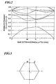
- This propagation characteristic may be explained with reference to a photonic band diagram which is similar to an electron band diagram in a semiconductor. For instance, in such a case where light is propagating through the photonic crystal region 102 as shown in Fig. 1 parallel to a plane of this drawing, and further, a plane of polarization of this light is located in parallel to the plane of this drawing, such a photonic band diagram (reduced zone scheme) as shown in Fig. 2 is obtained.
- a normalized frequency band (namely, photonic band gap), in which light can not be propagated through a photonic crystal, within a photonic band.
- a normalized frequency band from 0.29 to 0.45 corresponds to the photonic band gap.
- a normalized frequency band from 0.45 to 0.80 there is such light propagated through the photonic crystal region 102 toward a minus direction of the Y-axis (namely, wave vectors of point " ⁇ " to point "M").
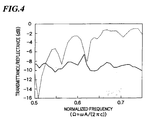
- the inventors of the present invention calculated both a transmittance and a reflectance on the basis of intensity of light obtained from the following simulation. That is, Gaussian distribution pulse light belonging to the normalized frequency band from 0.5 to 0.75 as shown in Fig. 2 is propagated toward an arrow direction as shown in Fig. 1, and the intensity of the light is simulated at a position P which is just after the Gaussian distribution pulse light had been projected from the photonic crystal region 102.
- Both the transmittance and a reflectance were calculated based upon the intensity of light obtained from a simulation. It should also be noted that this simulation has been carried out by employing the FDTD (finite difference time domain) method which is generally utilized in a numeral analysis of a photonic crystal.
- FDTD finite difference time domain
- Fig. 4 graphically represents a relationship among the normalized frequency, the transmittance, and the reflectance, which are obtained in the above-explained calculation.
- a solid line indicates the transmittance
- a broken line indicates the reflectance.
- the transmittance is equal to -8dB to -10dB.
- intensity of the light measured after transmitting through the photonic crystal region 102 is dropped by appropriately 1 digit than intensity of the light measured before transmitting through it.
- the reflectance of the light at the boundary surface of the photonic crystal region 102 is high, which light belongs to the propagation region of this photonic crystal region 102.
- a reflection loss occurred at the boundary surface of the photonic crystal region 102 may constitute a main reason why the intensity of the light transmitting through this photonic crystal region 102 is lowered.
- Such a reflection loss is improper in the case where the transmission light belonging to the propagation region of the photonic crystal is utilized because the S/N ratio of the output signal would be deteriorated, and further, the high power of the light source should be required.
- the refractive index N of the material of the normal medium region is equal to 3.065, a ratio of this refractive index N to the averaged refractive index N AV becomes 2.3, namely represents a large value.
- the inventors of the present invention have tried to increase transmittances of light which belongs to the propagation region of the photonic crystal by interposing the below-mentioned intermediate region between the normal medium region and the photonic crystal region.
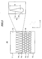
- Fig. 5 is a plan view schematically showing a structure of an optical element according to the present invention.
- an optical element 10 is arranged in such a manner that a photonic crystal region 13 is formed at a central portion of a substrate 11 including silicon as a medium, and furthermore, an intermediate 14 is formed -between a normal medium region 12 located at an upper portion of the substrate 11 and the photonic crystal region 13.
- a plurality of holes 15 having cylinder shapes are arranged in a two-dimensional triangular lattice shape, and these holes 15 are filled with air.
- holes 16 having projection portions 17 are arranged at an regular interval along one lateral column (namely, plus direction of the X-axis).
- the projection portions 17 are tapered and have sharp edges toward the normal medium region 12 , and lower halves of the projection portions 17 are united to semi-cylindrical portions 18. Similar to the photonic crystal region 13, these holes 16 are filled with air.
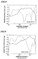
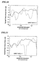
- Figs. 6-15 are graphic diagrams graphically showing relations among normalized frequencies, transmittances, and reflectances in the respective cases where the aspect ratios are selected to be one to ten. It should also be noted that in these graphic diagrams, a solid line indicates a transmittance, and a broken line indicates a reflectance. As shown in these graphic representations, the following fact can be seen.
- the aspect ratio when the aspect ratio is selected to be larger than, or equal to 3, the transmittances of the light belonging to the propagation region of the photonic crystal with respect to this photonic crystal are increased over a wide portion of the propagation range (namely, a normalized frequency band from 0.5 to 0.75) of this photonic crystal.
- the transmittance may be improved by 4dB to 5dB in an average value.
- a ratio of an averaged refractive index of the intermediate region 14 to an averaged refractive index of the photonic crystal region 13 is selected to be smaller than 2.3.
- the refractive index in the intermediate region 14 is gradually decreased from the refractive index of the normal medium region 12 to the averaged refractive index of the photonic crystal region 13.
- the mismatching problem of the impedance occurred between the normal medium region 12 and the photonic crystal region 13 may be gradually solved in the intermediate region 14, so that the reflection loss of the light produced at the boundary of the photonic crystal region 13 can be suppressed.
- the arrangement form of the holes in the photonic crystal region is not limited to such a two-dimensional triangular lattice form as shown in Fig. 2, but also may be realized by other two-dimensionally periodic forms (for example, two-dimensional cube-lattice form), or three-dimensionally lattice forms. Even in the case where the holes are arranged in the above-described arrangement forms, since the first to third embodiments are applied thereto, similar effects may be achieved.
- the optical elements may be used as an optical modulation element, an optical deflection element, or an optical switching element.
- the optical elements may be used as an optical modulation element, an optical deflection element, or an optical switching element.
- electrodes are mounted on the respective edge surfaces of the photonic crystal region of the optical element in such a manner that these electrodes are opposite to each other, since electric fields are applied among these electrodes so as to change the refractive index of the photonic crystal region, both intensity and a direction of the light which passes through this photonic crystal region may be changed.
- the modulation operation of the light, the deflection operation of the light, and the switching operation of the light may be carried out.
- lithium niobate may be employed as a material whose refractive index may be changed by an electric field.
- the reflection loss of the light occurred at the boundary surface between the photonic crystal and the normal medium can be suppressed, and thus, an optical element having the superior transmission characteristic can be provided.
Applications Claiming Priority (2)
| Application Number | Priority Date | Filing Date | Title |
|---|---|---|---|
| JP2000265433 | 2000-09-01 | ||
| JP2000265433A JP3923244B2 (ja) | 2000-09-01 | 2000-09-01 | 光素子 |
Publications (3)
| Publication Number | Publication Date |
|---|---|
| EP1184690A2 EP1184690A2 (en) | 2002-03-06 |
| EP1184690A3 EP1184690A3 (en) | 2004-05-12 |
| EP1184690B1 true EP1184690B1 (en) | 2006-04-05 |
Family
ID=18752701
Family Applications (1)
| Application Number | Title | Priority Date | Filing Date |
|---|---|---|---|
| EP01120593A Expired - Lifetime EP1184690B1 (en) | 2000-09-01 | 2001-08-29 | Optical element |
Country Status (4)
| Country | Link |
|---|---|
| US (1) | US6522448B2 (ja) |
| EP (1) | EP1184690B1 (ja) |
| JP (1) | JP3923244B2 (ja) |
| DE (1) | DE60118475T2 (ja) |
Families Citing this family (15)
| Publication number | Priority date | Publication date | Assignee | Title |
|---|---|---|---|---|
| TWI228179B (en) * | 1999-09-24 | 2005-02-21 | Toshiba Corp | Process and device for producing photonic crystal, and optical element |
| US6822784B2 (en) * | 2001-03-22 | 2004-11-23 | Matsushita Electric Works, Ltd | Light-beam deflecting device with photonic crystal, optical switch using the same, and light-beam deflecting method |
| JP3743637B2 (ja) * | 2001-08-23 | 2006-02-08 | 独立行政法人理化学研究所 | フォトニック結晶および光導波素子 |
| US6791732B2 (en) * | 2002-06-20 | 2004-09-14 | Agilent Technologies, Inc. | Systems and methods for altering the propagation of optical signals within optical media |
| CN1668948A (zh) * | 2002-07-08 | 2005-09-14 | 日本板硝子株式会社 | 光子晶体光波导 |
| JP4254189B2 (ja) * | 2002-10-02 | 2009-04-15 | 株式会社ニコン | 光学素子、分光装置、及び集光装置 |
| JP2004258169A (ja) * | 2003-02-25 | 2004-09-16 | Alps Electric Co Ltd | 光偏向素子及びそれを用いた光スイッチ |
| CN100351652C (zh) * | 2003-06-05 | 2007-11-28 | 株式会社村田制作所 | 三维周期构造体以及其制备方法 |
| JP3721181B2 (ja) | 2003-08-29 | 2005-11-30 | 独立行政法人科学技術振興機構 | 電磁波周波数フィルタ |
| US20050084195A1 (en) * | 2003-10-15 | 2005-04-21 | Hamann Hendrik F. | Method and apparatus for forming lateral electrical contacts for photonic crystal devices |
| JP4964123B2 (ja) * | 2004-04-16 | 2012-06-27 | ディ.ケイ. アンド イー.エル. マクフェイル エンタープライジーズ プロプライエタリー リミテッド | 空洞構造を備えた、調節可能フォトニック結晶として使用される光学的活性素子の形成方法 |
| JP4535373B2 (ja) * | 2004-08-02 | 2010-09-01 | 国立大学法人横浜国立大学 | 光学素子、光学素子への光の入射方法、及び、スーパープリズム |
| JP2007017494A (ja) * | 2005-07-05 | 2007-01-25 | Sharp Corp | フォトニック結晶導波路 |
| JP4956741B2 (ja) * | 2006-08-08 | 2012-06-20 | 国立大学法人京都工芸繊維大学 | フォトニック結晶導波路 |
| JP5152721B2 (ja) * | 2008-03-24 | 2013-02-27 | 国立大学法人横浜国立大学 | 半導体レーザ |
Family Cites Families (12)
| Publication number | Priority date | Publication date | Assignee | Title |
|---|---|---|---|---|
| DE19610656A1 (de) * | 1996-03-05 | 1997-09-11 | Deutsche Telekom Ag | Optische Mehrwege-Weiche mit elektrisch einstellbaren Photonenkristallen |
| EP1007998A1 (en) * | 1997-02-11 | 2000-06-14 | Massachusetts Institute Of Technology | Polymeric photonic band gap materials |
| DE59811997D1 (de) * | 1997-03-29 | 2004-10-28 | Deutsche Telekom Ag | Faser-integrierte photonenkristalle und -systeme |
| GB9710062D0 (en) * | 1997-05-16 | 1997-07-09 | British Tech Group | Optical devices and methods of fabrication thereof |
| US20010012149A1 (en) * | 1997-10-30 | 2001-08-09 | Shawn-Yu Lin | Optical elements comprising photonic crystals and applications thereof |
| US5999308A (en) * | 1998-04-01 | 1999-12-07 | Massachusetts Institute Of Technology | Methods and systems for introducing electromagnetic radiation into photonic crystals |
| US6040936A (en) * | 1998-10-08 | 2000-03-21 | Nec Research Institute, Inc. | Optical transmission control apparatus utilizing metal films perforated with subwavelength-diameter holes |
| JP4536866B2 (ja) * | 1999-04-27 | 2010-09-01 | キヤノン株式会社 | ナノ構造体及びその製造方法 |
| JP3456166B2 (ja) * | 1999-06-23 | 2003-10-14 | 日本電気株式会社 | フォトニック結晶を用いた光結合素子および光結合方法 |
| US20020070352A1 (en) * | 1999-11-30 | 2002-06-13 | Douglas C Allan | Creation of three-dimensional structures using ultrashort low energy laser exposure and structures formed thereby |
| US6542682B2 (en) * | 2000-08-15 | 2003-04-01 | Corning Incorporated | Active photonic crystal waveguide device |
| JP2002071982A (ja) * | 2000-09-01 | 2002-03-12 | Fuji Photo Film Co Ltd | 光素子、光偏向素子、光合波素子及び走査装置 |
-
2000
- 2000-09-01 JP JP2000265433A patent/JP3923244B2/ja not_active Expired - Fee Related
-
2001
- 2001-08-29 DE DE60118475T patent/DE60118475T2/de not_active Expired - Lifetime
- 2001-08-29 EP EP01120593A patent/EP1184690B1/en not_active Expired - Lifetime
- 2001-08-30 US US09/941,740 patent/US6522448B2/en not_active Expired - Fee Related
Also Published As
| Publication number | Publication date |
|---|---|
| DE60118475D1 (de) | 2006-05-18 |
| JP3923244B2 (ja) | 2007-05-30 |
| US20020041425A1 (en) | 2002-04-11 |
| EP1184690A3 (en) | 2004-05-12 |
| US6522448B2 (en) | 2003-02-18 |
| DE60118475T2 (de) | 2006-11-16 |
| JP2002071981A (ja) | 2002-03-12 |
| EP1184690A2 (en) | 2002-03-06 |
Similar Documents
| Publication | Publication Date | Title |
|---|---|---|
| EP1184690B1 (en) | Optical element | |
| US10359684B2 (en) | Optical waveguide element and optical modulator using the same | |
| JP4936313B2 (ja) | 光変調素子 | |
| US6731846B2 (en) | Dispersion compensator and optical transmission system using same | |
| CN100487503C (zh) | 光子学晶体装置 | |
| US10585328B2 (en) | Optical waveguide element and optical modulator using the same | |
| US20040008945A1 (en) | Waveguide bends and splitters in slab photonic crystals with noncircular holes | |
| US8948551B2 (en) | Reducing loss at intersection in optical waveguides | |
| CN113219584B (zh) | 一种基于高阶拓扑光子晶体的二次谐波控制器件 | |
| CA1273514A (en) | Optical waveguide devices | |
| US7336879B2 (en) | Two-dimensional photonic crystal slab, two-dimensional photonic crystal waveguide, and optical device | |
| CN114967188A (zh) | 一种二维六方晶格声子晶体及其波导结构 | |
| CN112255724A (zh) | 基于铌酸锂的波导阵列及其制造方法 | |
| JP4327797B2 (ja) | 二次元フォトニック結晶、ならびにそれを用いた導波路および共振器 | |
| CN111736405B (zh) | 一种基于圆形空气洞超构材料的纠缠光子对产生系统 | |
| Shinya et al. | Two-dimensional Si photonic crystals on oxide using SOI substrate | |
| CN110426772B (zh) | 一种可实现椭圆偏振光单向传输的光子晶体异质结构 | |
| US6768575B2 (en) | Optical deflection element | |
| US6374018B1 (en) | Optical switch, method of operating optical switch, and method of designing optical switch | |
| TWI767511B (zh) | 一種強健性共軛對稱光學元件及其設計方法 | |
| US6226427B1 (en) | Optical isolator | |
| JP2005250398A (ja) | フォトニック結晶光導波路およびこれを利用した光回路 | |
| CN217587667U (zh) | 一种菱圆混合型一维光子晶体纳米梁微腔结构 | |
| CN114725640B (zh) | 一种微波拓扑无阻传输线 | |
| US6327404B1 (en) | Wavelength filter |
Legal Events
| Date | Code | Title | Description |
|---|---|---|---|
| PUAI | Public reference made under article 153(3) epc to a published international application that has entered the european phase |
Free format text: ORIGINAL CODE: 0009012 |
|
| AK | Designated contracting states |
Kind code of ref document: A2 Designated state(s): AT BE CH CY DE DK ES FI FR GB GR IE IT LI LU MC NL PT SE TR |
|
| AX | Request for extension of the european patent |
Free format text: AL;LT;LV;MK;RO;SI |
|
| PUAL | Search report despatched |
Free format text: ORIGINAL CODE: 0009013 |
|
| RIC1 | Information provided on ipc code assigned before grant |
Ipc: 7G 02B 6/12 A |
|
| AK | Designated contracting states |
Kind code of ref document: A3 Designated state(s): AT BE CH CY DE DK ES FI FR GB GR IE IT LI LU MC NL PT SE TR |
|
| AX | Request for extension of the european patent |
Extension state: AL LT LV MK RO SI |
|
| 17P | Request for examination filed |
Effective date: 20040726 |
|
| AKX | Designation fees paid |
Designated state(s): DE FR GB |
|
| GRAP | Despatch of communication of intention to grant a patent |
Free format text: ORIGINAL CODE: EPIDOSNIGR1 |
|
| GRAS | Grant fee paid |
Free format text: ORIGINAL CODE: EPIDOSNIGR3 |
|
| GRAA | (expected) grant |
Free format text: ORIGINAL CODE: 0009210 |
|
| AK | Designated contracting states |
Kind code of ref document: B1 Designated state(s): DE FR GB |
|
| RAP1 | Party data changed (applicant data changed or rights of an application transferred) |
Owner name: FUJI PHOTO FILM CO., LTD. |
|
| REG | Reference to a national code |
Ref country code: GB Ref legal event code: FG4D |
|
| RIN1 | Information on inventor provided before grant (corrected) |
Inventor name: TANI, TAKEHARU Inventor name: BABA, TOSHIHIKO |
|
| REF | Corresponds to: |
Ref document number: 60118475 Country of ref document: DE Date of ref document: 20060518 Kind code of ref document: P |
|
| ET | Fr: translation filed | ||
| PLBE | No opposition filed within time limit |
Free format text: ORIGINAL CODE: 0009261 |
|
| STAA | Information on the status of an ep patent application or granted ep patent |
Free format text: STATUS: NO OPPOSITION FILED WITHIN TIME LIMIT |
|
| 26N | No opposition filed |
Effective date: 20070108 |
|
| REG | Reference to a national code |
Ref country code: GB Ref legal event code: 732E |
|
| REG | Reference to a national code |
Ref country code: FR Ref legal event code: CD Ref country code: FR Ref legal event code: TP |
|
| PGFP | Annual fee paid to national office [announced via postgrant information from national office to epo] |
Ref country code: GB Payment date: 20120829 Year of fee payment: 12 |
|
| PGFP | Annual fee paid to national office [announced via postgrant information from national office to epo] |
Ref country code: DE Payment date: 20120822 Year of fee payment: 12 Ref country code: FR Payment date: 20120823 Year of fee payment: 12 |
|
| GBPC | Gb: european patent ceased through non-payment of renewal fee |
Effective date: 20130829 |
|
| PG25 | Lapsed in a contracting state [announced via postgrant information from national office to epo] |
Ref country code: DE Free format text: LAPSE BECAUSE OF NON-PAYMENT OF DUE FEES Effective date: 20140301 |
|
| REG | Reference to a national code |
Ref country code: DE Ref legal event code: R119 Ref document number: 60118475 Country of ref document: DE Effective date: 20140301 |
|
| REG | Reference to a national code |
Ref country code: FR Ref legal event code: ST Effective date: 20140430 |
|
| PG25 | Lapsed in a contracting state [announced via postgrant information from national office to epo] |
Ref country code: GB Free format text: LAPSE BECAUSE OF NON-PAYMENT OF DUE FEES Effective date: 20130829 |
|
| PG25 | Lapsed in a contracting state [announced via postgrant information from national office to epo] |
Ref country code: FR Free format text: LAPSE BECAUSE OF NON-PAYMENT OF DUE FEES Effective date: 20130902 |