BACKGROUND OF THE INVENTION
1. Field of the Invention
The present invention relates to an optical deflection element which causes light rays having different wavelengths to exit in different directions, and more particularly to an optical deflection element which employs a photonic crystal.
2. Description of a Related Art
Heretofore, a passive element such as a prism or a diffraction grating has been employed as an optical deflection element. However, since the passive element such as a prism or a diffraction grating has a narrow deflection angle in causing light to exit therefrom, it requires a long optical path in order to satisfactorily split light rays having different wavelengths. Accordingly, in an apparatus which includes the optical deflection element for deflecting the light rays having different wavelengths in a wide range, it has been necessary to enlarge the element itself or to enlarge the whole apparatus for the purpose of gaining the long optical path.
Besides, in recent years, photonic crystals which exhibit unique dispersion characteristics as compared with conventional optical crystals have also been employed. The characteristics exhibited by the photonic crystals are stated in, for example, H. Kosaka et al. “Superprism phenomena in photonic crystals”, Physical Review B Vol. 58, No. 16, R10 096 to R10 099, 15 Oct. 1998-II), H. Kosaka et al. “Photonic crystals for micro lightwave circuits using wavelength-dependent angular beam steering” (Applied Physics Letters Vol. 74, No. 10, P. 1370-1372, 8 Mar. 1999, and Japanese Patent Application Laid-Open Publication JP-P2000-66002A.
Further, Japanese Patent Application Laid-Open Publication JP-P2000-56146A discloses a self-waveguide optical circuit in which photonic crystals are disposed at the main points of a substrate, whereby light is propagated in self-waveguiding fashion within the substrate so as to be split into a desired number of light rays. Furthermore, Japanese Patent Application Laid-Open Publication JP-A-11-271541 discloses a wavelength splitting circuit including two clads and a photonic crystal as its materials, for splitting light for every wavelength component owing to a structure in which the photonic crystal is interposed between the two clads.
The photonic crystal has been made smaller in size and higher in performance than the prism, the diffraction grating or the like by utilizing a superprism effect, but it still has a problem as stated below. Although the angle of light within the photonic crystal is greatly changed by a slight wavelength change, not only wavelength dispersion but also incident angle dispersion is great under the working conditions of the prior-art circuits disclosed in the above-mentioned patents, and hence, a high wavelength resolution cannot be attained considering the angular spread of an incident beam.
SUMMARY OF THE INVENTION
The present invention has been made in view of such a problem. An object of the present invention is to find out design conditions and working conditions for heightening a wavelength resolution and realize a high wavelength resolution in a wide wavelength range, in an optical deflection element which employs a photonic crystal.
In order to accomplish the object, an optical deflection element according to the first aspect of the present invention consists in an optical deflection element for splitting light rays in accordance with a wavelength of incident light, comprising a photonic crystal having an entrance end face and an exit end face, and having a refractive index which periodically changes depending upon positions thereof, wherein the element includes a region in which a propagation angle θC of the incident light within the photonic crystal changes in accordance with the wavelength of the incident light having entered at an incident angle θIN into the entrance end face so as to split the light rays having different wavelengths in accordance with different beam positions on the exit end face caused by a change of the propagation angle θC based on the wavelength of the incident light, and a relationship among a wavelength λ of the incident light in vacuum, a lattice constant “A” of the photonic crystal, the incident angle θIN and the propagation angle θC satisfies (∂θC/∂(A/λ))/(∂θC/∂θIN)>10. Here, the element should preferably include the region in which the relationship (∂θC/∂(A/λ))/(∂θC/∂θIN)>10 is met, in the whole wavelength range where the element is used, that is, in the whole predetermined wavelength range.
Further, an optical deflection element according to the second aspect of the present invention consists in an optical deflection element for splitting light rays in accordance with a wavelength of incident light, comprising a photonic crystal having an entrance end face and an exit end face, and having a refractive index which periodically changes depending upon positions thereof, wherein the element includes a region in which a propagation angle θC of the incident light having a beam width 2w0 within the photonic crystal changes in accordance with the wavelength of the incident light having entered at an incident angle θIN into the entrance end face so as to split the light rays having different wavelengths in accordance with different beam positions on the exit end face caused by a change of the propagation angle θC based on the wavelength of the incident light, and a center wavelength λ of a wavelength range of the incident light in vacuum, a lattice constant “A” of the photonic crystal, a refractive index n of a material at the entrance end face, a wavelength resolution Δλ of the optical deflection element and an optical path length L along which the entered light propagates within the photonic crystal satisfy {(∂θC/∂(A/λ))/(∂θC/∂θIN)}·2λ3/(πnAw0)>Δλ, and πnw0 2/{λ·(∂θC/∂θIN)}<L.
According to the present invention, it is possible to enhance the wavelength resolution of an optical deflection element employing a photonic crystal and to heighten the functions of the optical deflection element. Besides, since the size of the crystal necessary for obtaining a predetermined wavelength resolution can be calculated, the crystal of unnecessarily large size need not be prepared. It is accordingly permitted to reduce the size of the element and to curtail the cost thereof.
BRIEF DESCRIPTION OF THE DRAWINGS
FIG. 1 is a plan view showing an optical deflection element using a semicolumnar photonic crystal containing silicon as its material;
FIG. 2 is a plan view showing the shape of a photonic crystal region in FIG. 1;
FIG. 3 is a photonic band diagram of the photonic crystal region in FIG. 1;
FIG. 4 is a diagram showing the first Brillouin zone of the photonic crystal region in FIG. 1;
FIG. 5 is a diagram for explaining a method in which the wave number vector and propagation direction of light propagating within a photonic crystal region are found by drawing a diagram, on the basis of the wave number vector of incident light;
FIG. 6 is a diagram showing the change of a full spread angle versus an incident beam width;
FIG. 7 is a plan view showing the shape of an optical deflection element according to the first embodiment of the present invention;
FIG. 8 is a diagram showing the first Brillouin zone of the photonic crystal region of the optical deflection element according to the first embodiment of the present invention;
FIGS. 9A-9C are diagrams in which the dispersion planes of the first band to the third band within the range of the first Brillouin zone are respectively displayed in gradation;
FIGS. 10A-10C are diagrams each showing an intracrystal propagation angle θC which has been evaluated on the basis of the gradient of the dispersion plane;
FIGS. 11A-11C are diagrams each showing a quantity 1/p which has been calculated on the basis of the intracrystal propagation angle θC;
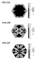
FIGS. 12A-12C are diagrams each showing a quantity q which has been calculated on the basis of the intracrystal propagation angle θC;
FIGS. 13A-13C are diagrams each showing a ratio q/p which has been calculated on the basis of the quantity 1/p and the quantity q;
FIG. 14 is a plan view showing the shape of the photonic crystal region of an optical deflection element according to the second embodiment of the present invention;
FIG. 15 is a diagram showing the first Brillouin zone of the photonic crystal region of the optical deflection element according to the second embodiment of the present invention;
FIGS. 16A-16C are diagrams in which the values of a ratio q/p for the first band to the third band are respectively shown within the range of the first Brillouin zone in the photonic crystal region;
FIG. 17 is a plan view showing the shape of the photonic crystal region of an optical deflection element according to the third embodiment of the present invention;
FIG. 18 is a diagram showing the first Brillouin zone of the photonic crystal region of the optical deflection element according to the third embodiment of the present invention;
FIGS. 19A-19C are diagrams in which the values of a ratio q/p for the first band to the third band are respectively shown within the range of the first Brillouin zone in the photonic crystal region;
FIG. 20 is a plan view showing the shape of the photonic crystal region of an optical deflection element according to the fourth embodiment of the present invention;
FIG. 21 is a diagram showing the first Brillouin zone of the photonic crystal region of the optical deflection element according to the fourth embodiment of the present invention;
FIGS. 22A-22C are diagrams in which the values of a ratio q/p for the first band to the third band are respectively shown within the range of the first Brillouin zone in the photonic crystal region;
FIG. 23 is a plan view showing the shape of the photonic crystal region of an optical deflection element according to the fifth embodiment of the present invention;
FIG. 24 is a diagram showing the first Brillouin zone of the photonic crystal region of the optical deflection element according to the fifth embodiment of the present invention; and
FIGS. 25A-25C are diagrams in which the values of a ratio q/p for the first band to the third band are respectively shown within the range of the first Brillouin zone in the photonic crystal region.
DESCRIPTION OF THE PREFERRED EMBODIMENTS
Now, embodiments of the present invention will be described with reference to the accompanying drawings. Incidentally, various numerical values used hereinbelow are merely values for the brevity of the description, and they shall be alterable to multifarious values within the scope of the present invention.
FIG. 1 is a plan view showing an optical deflection element which is formed of a semicolumnar photonic crystal containing silicon as its material. Light enters from an entrance end face 11 into a photonic crystal region 12 at an incident angle θIN, and propagates in the direction of an intracrystal propagation angle θC within the photonic crystal region 12. Besides, the light having propagated in the direction of the intracrystal propagation angle θC within the photonic crystal region 12 exits from an exit end face 13. As shown in FIG. 2, in the photonic crystal region 12, a plurality of cavities 16 each of which is in the shape of a column having a radius “r” are arranged in the shape of two-dimensional triangular lattice at a lattice constant “A” in parallel with the entrance end face 11, and they are filled up with air.
Next, there will be explained the intracrystal propagation angle θC of the light which propagates in the photonic crystal region 12. Here, it is assumed by way of example that the effective refractive index of silicon be 3.065, that the wavelength of the light to-be-handled in vacuum be 1.55 μm, that the radius “r” of each cavity 16 be 0.387 μm, and that the lattice constant “A” be 0.93 μm.
The propagation light in the photonic crystal is affected by multiple scattering ascribable to the periodic structure of this crystal, and its propagation characteristic is elucidated by a photonic band diagram which is similar to the band diagram of electrons in a semiconductor. In a case, for example, where light propagates in parallel with the sheet of the drawing within the photonic crystal region 12 in FIG. 1 and where its deflection plane is also parallel to the sheet of the drawing, a photonic band diagram (reduced zone scheme) as shown in FIG. 3 is obtained. Such a photonic band diagram affords the relationship between a wave number vector in a reciprocal space and a normalized frequency Ω=ωA/(2πc) where ω denotes the angular frequency of the light, and “c” the velocity of the light in vacuum.
Incidentally, symbols “Γ”, “J” and “X” affixed on the axis of abscissas in FIG. 3 denote specified wave number vectors in the first Brillouin zone as shown in FIG. 4.
FIG. 5 is a diagram for explaining a method in which the wave number vector and propagation direction of the light propagating within the photonic crystal region 12 are found by drawing a diagram, on the basis of the wave number vector of the light incident on the entrance end face 11 in FIG. 1.
In FIG. 5, an equifrequency dispersion plane ΣIN in the air and an equifrequency dispersion plane ΣC in the photonic crystal region 12 are shown. By the way, in FIG. 5, a kY-axis is accorded with the tangential direction of the entrance end face 11, and a kX-axis is accorded with the normal direction of the entrance end face 11.
As shown in FIG. 5, a vector kIN whose tail is the point Γ and whose head is a point PIN on the equifrequency dispersion plane ΣIN affords a wave number vector whose components are the coordinates of the point PIN. Besides, an outward normal vector VIN at the point PIN of the equifrequency dispersion plane ΣIN affords the direction in which the light of the wave number vector kIN propagates in the air. Likewise, a vector kC whose tail is the point Γ and whose head is a point PC on the equifrequency dispersion plane ΣC affords a wave number vector whose components are the coordinates of the point PC. Also, an outward normal vector VC at the point PC of the equifrequency dispersion plane ΣC affords the direction in which the light of the wave number vector kC propagates in the air. Incidentally, the sense of the vector VC is taken in the direction in which the sign of ∂ω/∂k becomes positive.
At the boundary surface between two different media, the component of the wave number vector tangential to this surface is conserved. Accordingly, the kY component of the wave number vector is conserved in FIG. 5.
The kIN component of the wave number vector is equal to the kY coordinate value of the intersection point between the kY-axis and a perpendicular (Snell line) SIN drawn from the point PIN down to the kY-axis. Accordingly, the vector kC whose tail is the point Γ and whose head is the intersection point PC between the equifrequency dispersion plane ΣC and the Snell line SIN affords the wave number vector of the light which propagates within the photonic crystal region 12 in FIG. 2. Besides, the angle θC which is defined between the kX-axis and the normal vector VC at the point PC of the equifrequency dispersion plane ΣC affords the angle of refraction of the light which is incident on the entrance end face 11 at the incident angle θIN. The light having the wave number vector kC propagates in the direction of the intracrystal propagation angle θC within the photonic crystal region 12 in FIG. 2.
Next, there will be explained a case where a Gaussian beam having a width 2w0 enters into the photonic crystal region 12. Here, it is assumed that the Gaussian beam form a beam waist at the entrance end face 11.
If the photonic crystal behaves like a free space of refractive index “n”, the beam width 2w of the Gaussian beam at the exit end face
13 is given by Eq. (1):
Here, λ denotes the wavelength of the Gaussian beam in vacuum. Besides, Δθ
0 denotes a half spread angle which the incident beam has at a great distance, and which is given by Eq. (2):
FIG. 6 is a diagram showing the change of a full spread angle 2Δθ0 versus the incident beam width 2w0, in the case of assuming the wavelength λ=1.55 μm and the effective refractive index n=3.065. As shown in FIG. 6, in order to make the full spread angle 2Δθ0 at most 1°, the incident beam width 2w0 needs to be set at 60 μm or so.
As shown in FIG. 5, however, the light undergoes the effect of being spread or collimated by the curvature of an equifrequency curve in the
photonic crystal region 12 unlike in the free space. This effect is represented by the quantity “p” of Eq. (3):
The incident Gaussian beam is the superposition of plane waves which have the angular spread as shown in FIG.
6. On condition that the half spread angle Δθ
0 is small, the spread Δθ
C of the light in the
photonic crystal region 12 is given by Δθ
C=(∂θ
C/∂θ
IN)Δθ
0=pΔθ
0. That is, the angular spread of the incident Gaussian beam changes “p” times in the
photonic crystal region 12. Accordingly, the beam width 2w at the exit end face
13 is given by Eq. (4):
Besides, an angle Δθ
OUT which this beam width occupies at a far exit position is given by Eq. (5):
Next, a quantity “q” which represents the rate of change of the intracrystal propagation angle θ
C in the case of slightly changing the wavelength λ shall be defined by Eq. (6):
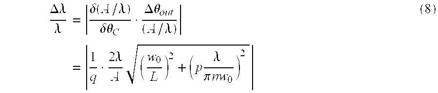
Here, A/λ denotes the normalized frequency of the photonic crystal. Besides, using the normalized frequency, a normalized wavelength width Δλ/λ which the photonic crystal can resolve is given by Eq. (7):
In this regard, Δθ
C denotes a spread which the Gaussian beam has in the
photonic crystal region 12, and actually the angle Δθ
OUT occupied at the exit end face
13 is an angle which can be effectively resolved. Therefore, the actual normalized wavelength width Δλ/λ is given by Eq. (8):
Here, on condition that Eq. (9) holds true, the normalized wavelength width Δλ/λ is given by Eq. (10):
As indicated by Eq. (10), as the value of a ratio p/q is smaller, the normalized wavelength width Δλ/λ becomes smaller, and hence, a wavelength resolution is enhanced more. Here, as the value of the quantity “p” becomes smaller, a collimating property is more intense, and more resolved points can be obtained, but an element length needs to be set great as indicated by Eq. (9). Besides, as the incident beam width w0 is greater, the wavelength resolution can be heightened more, but similarly the element length needs to be set great. Incidentally, the number of points at which wavelengths can be resolved (hereinbelow, termed “resolvable points”) is determined by the extent of a frequency range in which Eq. (10) satisfies a predetermined resolution.
Favorable for the application to the optical deflection element is a region where the ratio p/q is as small as possible and where the change of the ratio p/q in the case of changing the frequency with the incident angle fixed is small. The inventors, therefore, have set the design conditions such as a crystal size and the working conditions such as a beam size to realize a necessary resolution, by selecting the smallest possible incident beam width w0 in a range in which the necessary resolution and the necessary number of resolvable points are satisfied, as explained below.
FIG. 7 is a plan view showing the shape of an optical deflection element according to the first embodiment of the present invention.
As shown in FIG. 7, a semicolumnar photonic crystal region 12 having a radius L is formed centrally of a substrate 10 whose material is silicon. Light enters from the non-photonic crystal region (14) side of an entrance end face 11 into the photonic crystal region 12 at an incident angle θIN, and propagates in the direction of an intracrystal propagation angle θC within the photonic crystal region 12. Besides, the light having propagated in the direction of the intracrystal propagation angle θC within the photonic crystal region 12 exits into a non-photonic crystal region 15 at an exit end face 13. As shown in FIG. 2, in the photonic crystal region 12, a plurality of cavities 16 which are parallel to the entrance end face 11 and each of which is in the shape of a column having a radius “r” are arranged in the shape of two-dimensional triangular lattice at a lattice constant “A”. Besides, the entrance end face 11 is parallel to a Γ-J direction in the first Brillouin zone as shown in FIG. 8. In this embodiment, the effective refractive index “n” of the silicon substrate 10 is 3.065, the radius “r” of each cavity 16 is 0.312A, and the cavities 16 are filled up with air.
Such a photonic crystal region 12 is formed by, for example, depositing a resist on the non-photonic crystal regions 14, 15 and on the part of the photonic crystal region 12 not to be formed with the cavities 16, and thereafter subjecting the substrate 10 to dry etching of good perpendicularity.
Incidentally, a substance other than silicon (for example, polymer, sapphire, quartz or glass) may well be employed as the material of the substrate 10, and a medium other than the air as has a refractive index different from that of the substrate 10 (for example, polymer, dielectric or glass) may well be packed in the cavities 16.
FIGS. 9A-9C are diagrams in which the dispersion planes of the first band to the third band in the range of the first Brillouin zone of the photonic crystal region 12 are respectively displayed in gradation. Since the propagation direction of light within the photonic crystal region 12 becomes the normal direction of the equifrequency dispersion plane as shown in FIG. 5, the propagation directions of the light can be respectively found by computing the gradients of the dispersion planes shown in FIGS. 9A-9C.
FIGS. 10A-10C are diagrams showing intracrystal propagation angles θC which have been evaluated on the basis of the gradients of the dispersion planes as shown in FIGS. 9A-9C, respectively. Besides, lines in FIGS. 10A-10C indicate equi-incident angle lines. The equi-incident angle line indicates the change of an entrance condition within the photonic crystal region 12 in the case of changing the frequency under the condition that the incident angle θIN for the photonic crystal region 12 is constant. A central vertical line indicates a case where the incident angle θIN=0° holds, that is, where the light is normally incident, and lines carved every 5° on each of the right and left sides indicate cases where the incident angle θIN is changed. As shown in FIG. 5, the entrance condition at a specified incident angle and a specified frequency can be found by drawing the Snell line from the side on which the component of the wave number vector tangential to the entrance end face 11 is conserved.
FIGS. 11A-11C are diagrams showing the values of a quantity 1/p which have been respectively calculated on the basis of the intracrystal propagation angles θC as shown in FIGS. 10A-10C. As indicated by Eq. (3), the value of the quantity 1/p is calculated by computing the differential value “p” of the intracrystal propagation angle θC in a direction perpendicular to the equi-incident angle line, and then obtaining the reciprocal of the differential value “p”.
FIGS. 12A-12C are diagrams showing the values of a quantity “q” which have been respectively calculated on the basis of the intracrystal propagation angles θC as shown in FIGS. 10A-10C. As indicated by Eq. (6), the value of the quantity “q” is calculated by computing the differential of the intracrystal propagation angle θC in the gradient direction of the dispersion plane.
FIGS. 13A-13C are diagrams showing the values of a ratio q/p which have been respectively calculated on the basis of the values of the quantity 1/p as shown in FIGS. 11A-11C and the values of the quantity “q” as shown in FIGS. 12A-12C. FIGS. 13A-13C represent the characteristic that a higher wavelength resolution is demonstrated as the ratio q/p is greater (at a brighter part).
There has heretofore been deemed favorable that condition of an abrupt change under which the equifrequency dispersion plane is uneven as at the part between points C and D as shown in FIG. 4 of H. Kosaka et al. “Superprism phenomena in photonic crystals”, Physical Review B Vol. 58, No. 16, R10 096 to R10 099, 15 Oct. 1998-II. Such a part, however, does not accord with a part of high wavelength resolution.
Here, it is assumed that the wavelength of the light to-be-handled be 1550 nm, and that a necessary wavelength resolution Δλ be 1 nm. Also, it is assumed that a center normalized frequency be A/λ=0.4, in other words, that A=620 nm hold, and that q/p=10 hold in view of FIGS. 13A-13C. Then, the incident beam width w0 becomes nearly equal to 125 μm. Accordingly, when a beam having a width of at least 250 μm is entered into the photonic crystal, the necessary resolution is satisfied. Besides, the size of the crystal required on this occasion is calculated from Eq. (9). Assuming 1/p=2 in view of FIGS. 11A-11C, the size of the crystal needs to be at least 194 mm.
In addition, FIGS. 13A-13C represent the characteristic that, when the ratio q/p is observed along the equi-incident angle line, the high wavelength resolution is held in a wider wavelength range as the number of equifrequency lines intersecting with the equi-incident angle line is larger. By way of example, near that region of FIG. 13B which corresponds to the region of an incident angle of 10° to 11° and a normalized frequency of 0.39 to 0.41 as shown in FIG. 9B for the exemplary second band, a region where the ratio q/p continuously exceeds 10 is existent, and the high resolution is held in the range of the wavelength λ from about 1.51 μm to about 1.59 μm.
Next, further embodiments of the present invention will be described.
FIG. 14 is a plan view showing the shape of the photonic crystal region of an optical deflection element according to the second embodiment of the present invention. Besides, FIG. 15 is a diagram showing the first Brillouin zone of the photonic crystal region of the optical deflection element according to this embodiment. As shown in FIG. 14, a plurality of cavities 17 which are parallel to an entrance end face 11 and each of which is in the shape of a column having a radius “r” are arranged in the shape of two-dimensional triangular lattice at a lattice constant “A”. Besides, the entrance end face 11 is parallel to a Γ-X direction in the first Brillouin zone shown in FIG. 15. In this embodiment, the effective refractive index “n” of a silicon substrate 10 is 3.065, the radius “r” of each cavity 16 is 0.312A, and the cavities 17 are filled up with air.
FIGS. 16A-16C are diagrams in which the values of a ratio q/p for the first band to the third band are respectively shown within the range of the first Brillouin zone in the photonic crystal region. As shown in FIGS. 16A-16C, it is understood that regions of high resolutions exist also in this embodiment. As compared with those of the first embodiment, however, the number of equifrequency lines intersecting with each equi-incident angle line is smaller, and a frequency range satisfying the condition of high resolution is narrower. Accordingly, in a case where the optical deflection element is to be operated in a wide wavelength range, the use of the first embodiment in which the entrance face is parallel to the Γ-J direction is better.
FIG. 17 is a plan view showing the shape of the photonic crystal region of an optical deflection element according to the third embodiment of the present invention. In this embodiment, the sectional shape of each cavity is an ellipse which has a major axis perpendicular to an entrance end face 11. Besides, FIG. 18 shows the first Brillouin zone of the photonic crystal region of the optical deflection element according to this embodiment.
As shown in FIG. 17, a plurality of cavities 18 which are parallel to the entrance end face 11 are arranged in the shape of two-dimensional triangular lattice at a lattice constant “A”. Besides, the entrance end face 11 is parallel to a Γ-J direction in the first Brillouin zone as shown in FIG. 18. In this embodiment, the effective refractive index “n” of a silicon substrate 10 is 3.065, the major axis and minor axis of each cavity 18 are 0.9A and 0.4A, respectively, and the cavities 18 are filled up with air.
FIGS. 19A-19C are diagrams in which the values of a ratio q/p for the first band to the third band are respectively shown within the range of the first Brillouin zone in the photonic crystal region 12. As shown in FIGS. 19A-19C, it is understood that regions of high resolutions exist also in this embodiment. As compared with that of the first embodiment, a frequency range of high resolution widens more near the region of an incident angle of 10° for the second band, so that the third embodiment is usable in a wider wavelength range.
FIG. 20 is a plan view showing the shape of the photonic crystal region of an optical deflection element according to the fourth embodiment of the present invention. Besides, FIG. 21 is a diagram showing the first Brillouin zone of the photonic crystal region of the optical deflection element according to this embodiment.
As shown in FIG. 20, a plurality of cavities 19 which are parallel to an entrance end face 11 and each of which is in the shape of a column having a radius “r” are arranged in the shape of square lattice at a lattice constant “A”. Besides, the entrance end face 11 is parallel to a Γ-x direction in the first Brillouin zone as shown in FIG. 21. In this embodiment, the effective refractive index “n” of a silicon substrate 10 is 3.065, the radius “r” of each cavity 19 is 0.312A, and the cavities 19 are filled up with air.
FIGS. 22A-22C are diagrams in which the values of a ratio q/p for the first band to the third band are respectively shown within the range of the first Brillouin zone in the photonic crystal region 12. It is understood that regions of high resolutions exist also in this embodiment.
FIG. 23 is a plan view showing the shape of the photonic crystal region of an optical deflection element according to the fifth embodiment of the present invention.
As shown in FIG. 23, a plurality of cavities 20 which are parallel to an entrance end face 11 and each of which is in the shape of a column having a radius “r” are arranged in the shape of square lattice at a lattice constant “A”. Besides, the entrance end face 11 is parallel to a Γ-M direction in the first Brillouin zone shown in FIG. 24. In this embodiment, the effective refractive index “n” of a silicon substrate 10 is 3.065, the radius “r” of each cavity 20 is 0.312A, and the cavities 20 are filled up with air.
FIGS. 25A-25C are diagrams in which the values of a ratio q/p for the first band to the third band are respectively shown within the range of the first Brillouin zone in the photonic crystal region 12. It is understood that regions of high resolutions exist also in this embodiment. As compared with that of the fourth embodiment, a frequency range of high resolution widens more near the region of an incident angle of 8° for the second band, so that the fifth embodiment is usable in a wider wavelength range.
In this way, the optical deflection element which has the high wavelength resolution characteristic in the wide wavelength range can be designed by determining the shape of each cavity and the arrangement of the cavities in the photonic crystal region 12.
As described above, according to the present invention, it is possible to enhance the wavelength resolution of an optical deflection element employing a photonic crystal and to heighten the functions of the optical deflection element. Besides, since the size of the crystal necessary for obtaining a predetermined wavelength resolution can be calculated, the crystal of unnecessarily large size need not be prepared. It is accordingly permitted to reduce the size of the element and to curtail the cost thereof.