EP1180494A2 - Résonateurs à couches minces fabriqués sur des membranes manufacturées par évidement à partir de la face supérieure - Google Patents
Résonateurs à couches minces fabriqués sur des membranes manufacturées par évidement à partir de la face supérieure Download PDFInfo
- Publication number
- EP1180494A2 EP1180494A2 EP01306284A EP01306284A EP1180494A2 EP 1180494 A2 EP1180494 A2 EP 1180494A2 EP 01306284 A EP01306284 A EP 01306284A EP 01306284 A EP01306284 A EP 01306284A EP 1180494 A2 EP1180494 A2 EP 1180494A2
- Authority
- EP
- European Patent Office
- Prior art keywords
- resonator
- electrode
- wafer
- layer
- piezoelectric
- Prior art date
- Legal status (The legal status is an assumption and is not a legal conclusion. Google has not performed a legal analysis and makes no representation as to the accuracy of the status listed.)
- Granted
Links
- 239000012528 membrane Substances 0.000 title claims abstract description 33
- 239000010409 thin film Substances 0.000 title description 3
- 238000000034 method Methods 0.000 claims abstract description 50
- XUIMIQQOPSSXEZ-UHFFFAOYSA-N Silicon Chemical compound [Si] XUIMIQQOPSSXEZ-UHFFFAOYSA-N 0.000 claims abstract description 30
- 229910052710 silicon Inorganic materials 0.000 claims abstract description 30
- 239000010703 silicon Substances 0.000 claims abstract description 30
- 230000008569 process Effects 0.000 claims abstract description 20
- 238000005530 etching Methods 0.000 claims abstract description 19
- 238000002955 isolation Methods 0.000 claims description 35
- 230000004888 barrier function Effects 0.000 claims description 10
- XAGFODPZIPBFFR-UHFFFAOYSA-N aluminium Chemical compound [Al] XAGFODPZIPBFFR-UHFFFAOYSA-N 0.000 claims description 7
- 229910052782 aluminium Inorganic materials 0.000 claims description 7
- 238000000151 deposition Methods 0.000 claims description 5
- 238000001312 dry etching Methods 0.000 claims description 5
- 238000004544 sputter deposition Methods 0.000 claims description 4
- 238000000059 patterning Methods 0.000 claims description 3
- 238000004519 manufacturing process Methods 0.000 abstract description 24
- 239000011248 coating agent Substances 0.000 abstract 1
- 238000000576 coating method Methods 0.000 abstract 1
- VYPSYNLAJGMNEJ-UHFFFAOYSA-N silicon dioxide Inorganic materials O=[Si]=O VYPSYNLAJGMNEJ-UHFFFAOYSA-N 0.000 description 16
- 239000000463 material Substances 0.000 description 12
- 239000004065 semiconductor Substances 0.000 description 9
- 229910052681 coesite Inorganic materials 0.000 description 7
- 229910052906 cristobalite Inorganic materials 0.000 description 7
- 239000000377 silicon dioxide Substances 0.000 description 7
- 229910052682 stishovite Inorganic materials 0.000 description 7
- 229910052905 tridymite Inorganic materials 0.000 description 7
- 239000000945 filler Substances 0.000 description 6
- BLIQUJLAJXRXSG-UHFFFAOYSA-N 1-benzyl-3-(trifluoromethyl)pyrrolidin-1-ium-3-carboxylate Chemical compound C1C(C(=O)O)(C(F)(F)F)CCN1CC1=CC=CC=C1 BLIQUJLAJXRXSG-UHFFFAOYSA-N 0.000 description 5
- 230000008901 benefit Effects 0.000 description 4
- 238000013461 design Methods 0.000 description 4
- 239000000758 substrate Substances 0.000 description 4
- 238000005516 engineering process Methods 0.000 description 2
- 238000012986 modification Methods 0.000 description 2
- 230000004048 modification Effects 0.000 description 2
- 238000001020 plasma etching Methods 0.000 description 2
- 238000012545 processing Methods 0.000 description 2
- 239000010453 quartz Substances 0.000 description 2
- PIGFYZPCRLYGLF-UHFFFAOYSA-N Aluminum nitride Chemical compound [Al]#N PIGFYZPCRLYGLF-UHFFFAOYSA-N 0.000 description 1
- 230000001413 cellular effect Effects 0.000 description 1
- 238000004891 communication Methods 0.000 description 1
- 239000004020 conductor Substances 0.000 description 1
- PMHQVHHXPFUNSP-UHFFFAOYSA-M copper(1+);methylsulfanylmethane;bromide Chemical compound Br[Cu].CSC PMHQVHHXPFUNSP-UHFFFAOYSA-M 0.000 description 1
- 239000013078 crystal Substances 0.000 description 1
- BHEPBYXIRTUNPN-UHFFFAOYSA-N hydridophosphorus(.) (triplet) Chemical compound [PH] BHEPBYXIRTUNPN-UHFFFAOYSA-N 0.000 description 1
- 230000010354 integration Effects 0.000 description 1
- 239000007788 liquid Substances 0.000 description 1
- 238000005459 micromachining Methods 0.000 description 1
- 238000000206 photolithography Methods 0.000 description 1
- 238000005240 physical vapour deposition Methods 0.000 description 1
- 230000004044 response Effects 0.000 description 1
- 230000035939 shock Effects 0.000 description 1
- 239000005368 silicate glass Substances 0.000 description 1
Images

Classifications
-
- H—ELECTRICITY
- H03—ELECTRONIC CIRCUITRY
- H03H—IMPEDANCE NETWORKS, e.g. RESONANT CIRCUITS; RESONATORS
- H03H9/00—Networks comprising electromechanical or electro-acoustic devices; Electromechanical resonators
- H03H9/15—Constructional features of resonators consisting of piezoelectric or electrostrictive material
- H03H9/17—Constructional features of resonators consisting of piezoelectric or electrostrictive material having a single resonator
- H03H9/171—Constructional features of resonators consisting of piezoelectric or electrostrictive material having a single resonator implemented with thin-film techniques, i.e. of the film bulk acoustic resonator [FBAR] type
- H03H9/172—Means for mounting on a substrate, i.e. means constituting the material interface confining the waves to a volume
- H03H9/173—Air-gaps
-
- B—PERFORMING OPERATIONS; TRANSPORTING
- B81—MICROSTRUCTURAL TECHNOLOGY
- B81C—PROCESSES OR APPARATUS SPECIALLY ADAPTED FOR THE MANUFACTURE OR TREATMENT OF MICROSTRUCTURAL DEVICES OR SYSTEMS
- B81C1/00—Manufacture or treatment of devices or systems in or on a substrate
- B81C1/00015—Manufacture or treatment of devices or systems in or on a substrate for manufacturing microsystems
- B81C1/00134—Manufacture or treatment of devices or systems in or on a substrate for manufacturing microsystems comprising flexible or deformable structures
- B81C1/00142—Bridges
-
- H—ELECTRICITY
- H03—ELECTRONIC CIRCUITRY
- H03H—IMPEDANCE NETWORKS, e.g. RESONANT CIRCUITS; RESONATORS
- H03H3/00—Apparatus or processes specially adapted for the manufacture of impedance networks, resonating circuits, resonators
- H03H3/007—Apparatus or processes specially adapted for the manufacture of impedance networks, resonating circuits, resonators for the manufacture of electromechanical resonators or networks
- H03H3/02—Apparatus or processes specially adapted for the manufacture of impedance networks, resonating circuits, resonators for the manufacture of electromechanical resonators or networks for the manufacture of piezoelectric or electrostrictive resonators or networks
-
- B—PERFORMING OPERATIONS; TRANSPORTING
- B81—MICROSTRUCTURAL TECHNOLOGY
- B81B—MICROSTRUCTURAL DEVICES OR SYSTEMS, e.g. MICROMECHANICAL DEVICES
- B81B2201/00—Specific applications of microelectromechanical systems
- B81B2201/02—Sensors
- B81B2201/0271—Resonators; ultrasonic resonators
-
- B—PERFORMING OPERATIONS; TRANSPORTING
- B81—MICROSTRUCTURAL TECHNOLOGY
- B81C—PROCESSES OR APPARATUS SPECIALLY ADAPTED FOR THE MANUFACTURE OR TREATMENT OF MICROSTRUCTURAL DEVICES OR SYSTEMS
- B81C2201/00—Manufacture or treatment of microstructural devices or systems
- B81C2201/01—Manufacture or treatment of microstructural devices or systems in or on a substrate
- B81C2201/0101—Shaping material; Structuring the bulk substrate or layers on the substrate; Film patterning
- B81C2201/0128—Processes for removing material
- B81C2201/013—Etching
- B81C2201/0135—Controlling etch progression
- B81C2201/014—Controlling etch progression by depositing an etch stop layer, e.g. silicon nitride, silicon oxide, metal
-
- H—ELECTRICITY
- H03—ELECTRONIC CIRCUITRY
- H03H—IMPEDANCE NETWORKS, e.g. RESONANT CIRCUITS; RESONATORS
- H03H3/00—Apparatus or processes specially adapted for the manufacture of impedance networks, resonating circuits, resonators
- H03H3/007—Apparatus or processes specially adapted for the manufacture of impedance networks, resonating circuits, resonators for the manufacture of electromechanical resonators or networks
- H03H3/02—Apparatus or processes specially adapted for the manufacture of impedance networks, resonating circuits, resonators for the manufacture of electromechanical resonators or networks for the manufacture of piezoelectric or electrostrictive resonators or networks
- H03H2003/021—Apparatus or processes specially adapted for the manufacture of impedance networks, resonating circuits, resonators for the manufacture of electromechanical resonators or networks for the manufacture of piezoelectric or electrostrictive resonators or networks the resonators or networks being of the air-gap type
Definitions
- This invention relates to electrical bulk resonators and more particularly to a method for manufacturing a thin film resonator on a membrane over a cavity on a semiconductor substrate as part of a monolithic integrated circuit.
- radio receivers particularly paging receivers, cellular radios, and microwave satellite communication systems
- components which form the system to take up as little space as possible. It is desirable for as many components as possible to be integrated into a single integrated circuit in the form of monolithic circuits.
- a monolithic integrated system requires less space, is more reliable, has a lower power consumption, has more precise temperature control, and has a higher shock tolerance, than one which requires multiple independent components. It is also easier to produce matched resonator and oscillator circuits when they are produced on the same substrate, and, typically monolithic structures present lower manufacturing costs at every stage of design and production. Thus the advantages of monolithic integration are numerous.
- An important element used in the type of equipment mentioned above is an electronic filter.
- the present state of the art employs resonant electromechanical structures in designing such filters.
- the structures and materials used depend on the frequencies of the signals involved, and can be separated into three major categories, (a) mechanical, (b) quartz crystals and (c) piezoelectric materials.
- Such resonators may be one of two basic types, a surface acoustic resonator (SAW) or a bulk acoustic resonator (BAW). SAW resonators don't respond well at frequencies above 2GHz, and are not able to handle radio frequency (RF) signals at high power.
- SAW surface acoustic resonator
- BAW bulk acoustic resonator
- BAW resonators on the other hand, do not suffer such limitations.
- BAW resonators in their basic form comprise a piezoelectric material sandwiched between two opposing electrodes.
- Such resonators in order to perform with the required efficiency require an unsupported structure, which means that when such resonators are used as a part of an integrated circuit structure, such as a CMOS, they should be placed either over a cavity in the semiconductor support, or should be elevated therefrom.
- BAW resonators in order to be commercially useful, should be able to be manufactured as part of the normal CMOS and Bipolar silicon processing techniques.
- unsupported mechanical, quartz and piezoelectric electromechanical resonators may be constructed on a support such as a silicon semiconductor wafer, by first micro-machining a cavity in the substrate and filling the cavity with a sacrificial non silicon filler such as a phosphorous silicate glass (PSG).
- a sacrificial non silicon filler such as a phosphorous silicate glass (PSG).
- PSG phosphorous silicate glass
- the resonator is next built on the sacrificial filler and extends beyond the cavity limits to the substrate surface.
- the filler provides support during the manufacturing steps. Once the resonator structure is completed the sacrificial filler is removed by etching. The result is a BAW resonator that is constructed over a cavity and is, therefore substantially unsupported.
- the disclosed resonator offers advantages over prior resonators, the ' method of its fabrication, which requires first creating the cavity, then filling and finally etching the filler away from under the resonator itself, is not a method that can be readily incorporated in the traditional fabrication techniques used in the fabrication of monolithic integrated circuits. Further more, the etching process to remove the filler material disclosed in the prior art is a liquid etching process which also attacks aluminum and which sometimes washes away small parts of the circuit.
- an object of the present invention to provide a method and resulting resonator whose manufacturing steps may be readily integrated in a typical CMOS or Bipolar Silicon processing or added to such process as a post process step.
- the above object is obtained in accordance with this invention through a new bulk resonator incorporated in the traditional fabrication techniques used in the fabrication of monolithic integrated circuits on a wafer.
- the resonator is decoupled from the wafer by a cavity etched under the resonator using selective etching through front openings (vias) in a resonator membrane.
- the resonator may be a bulk type resonator, fabricated on a semiconductor wafer support preferably using a piezoelectric material, having the following structure:
- the isolation layer may be a high resistivity layer.
- Such structure may be fabricated to generate a bulk resonator structure on a wafer by a method comprising the steps of:
- step (C) a plurality of vias are opened, surrounding the first electrode and the dry etching step is a gaseous etch process.
- the etching step preferably uses xenon difluoride (XeF 2 ).
- a bulk acoustic resonator on a silicon wafer with electrodes made of Al, and a AlN piezoelectric membrane.
- the membrane is self supporting and extends completely over a cavity etched under the electrodes in the supporting wafer.
- the membrane is isolated from the silicon semiconductor wafer surface by a high resistivity sputtered silicon layer deposited between the membrane undersurface and the silicon support surface, and includes a plurality of vias extending therethrough located adjacent to and around said electrodes.
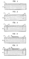
- Figure 1 shows in schematic elevation a portion of a wafer on which there is to be constructed a BAW resonator following a first step of a process to manufacture such resonator in accordance with this invention.
- Figure 2 shows in schematic elevation the same portion of the wafer shown in figure 1 following a second step of the process to manufacture such resonator in accordance with this invention.
- Figure 3 shows in schematic elevation the same portion of the wafer shown in figure 2 following a third step of the process to manufacture such resonator in accordance with this invention.
- Figure 4 shows in schematic elevation the same portion of the wafer shown in figure 3 following a fourth step of the process to manufacture such resonator in accordance with this invention.
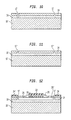
- Figure 5 shows in schematic elevation the same portion of the wafer shown in figure 4 following a fifth step of the process to manufacture such resonator in accordance with this invention.
- Figure 6 shows in schematic elevation the same portion of the wafer shown in figure 5 following a sixth step of the process to manufacture such resonator in accordance with this invention.
- Figure 7 shows in schematic elevation the same portion of the wafer shown in figure 6 following a seventh step of the process to manufacture such resonator in accordance with this invention.
- Figure 8 shows in schematic elevation the same portion of the wafer with the resonator structure completed.
- Figure 9 is a schematic top view of the resonator structure depicted in figure 8.
- Figure 10 shows in schematic elevation a wafer portion prepared for use in fabricating a resonator according with an alternate embodiment of this invention.
- Figure 11 shows in schematic elevation the same portion of the wafer shown in figure 10 following a second step of the process used to manufacture the alternate embodiment of the invention.
- Figure 12 shows in schematic elevation the same portion of the wafer shown in figure 11 with the alternate embodiment of the resonator completed.
- a semiconductor support 10 which is preferably a silicon wafer.
- a surface 12 of the wafer there is, preferably, deposited using conventional technology such as sputtering, an optional silicon layer to form a isolation layer 14.
- this layer is between about 2*10 -6 and 5*10 -6 meters thick.
- a trench 16 (or a series of trenches) is next etched through the isolation layer 14 and into the silicon wafer delineating a desired area 17 as better shown in figures 2 and 9. Etching of the trenches is preferably done using the well known Reactive Ion Etching technology, (RIE).
- RIE Reactive Ion Etching technology
- the trenches are next filled with low temperature oxide (LTO), to produce an etch delimiting barrier 16' which is used in later step to contain the etching of the wafer and isolation layer to within the area within the desired area 17.
- LTO low temperature oxide
- a conductive layer such as aluminum is next deposited to a typical thickness of between about 0.2*10 -6 and 0.3*10 -6 meters over the isolation layer and patterned (masked and etched according to a desired pattern using photolithography) to form a first electrode 18 on the surface of the isolation layer within the desired area 17, as shown in figure 4.
- a layer 20 of a piezoelectric material such as a layer of AIN.
- the piezoelectric AIN layer is deposited to a thickness of about 1*10 -6 and 5*10 -6 meters, preferably 2.7*10 -6 meters. However the thickness of the piezoelectric material may be different depending on the design frequency response of the resonator.
- a second conductive layer again preferably an aluminum layer is deposited over the piezoelectric layer and patterned to form a second electrode 22 substantially coextensive and over the first electrode 18, as shown in figure 7.
- connector or bond pads 24 and optionally 24' are formed also over the piezoelectric material, preferably outside the desired area 17 delimited by the trenches filled with LTO. These pads are connected to the second electrode through a conductive path 23 and 23' respectively, which is also preferably formed by photolithographic patterning simultaneously with the second electrode and bond pads.
- the bond pads serve as external connection points for accessing the resonator.
- Both the electrodes, conductive paths, bonding pads and the piezoelectric layer are preferably deposited using physical vapor deposition or sputtering.
- the size of the electrodes will vary. Typical dimensions for a square shaped electrode pair are between 100*10 -6 and 400*10 -6 meters for the sides.
- a number of vias 26 are formed, preferably by etching, through the piezoelectric material within the desired area 17.
- the vias are placed adjacent the electrodes and preferably evenly spaced all around the electrodes.
- Typical via diameters are between 5*10 -6 and 20*10 -6 meters, preferably about 10*10 -6 meters and extend through the piezoelectric layer to the surface of the isolation layer 14.
- the next step, illustrated in figure 8, is the etching of a cavity 28 under the first and second electrodes so as to isolate from the support 10 the bulk resonator formed by the three layer combination of the first electrode 18, piezoelectric layer 20 and second electrode 22.
- This is accomplished in a dry etching process by introducing through the vias 26 an etchant, which is preferably a gaseous etchant that attacks the isolation layer and may also attack the underlying support, but does not attack the piezoelectric material or the electrodes.
- a bulk acoustic resonator is formed using aluminum as the conductive material for the first and second electrodes and aluminum nitride (AlN) for the piezoelectric material.
- the support is a silicon wafer and the isolation layer is a high resistivity layer such as a silicon layer between the piezoelectric layer and the wafer surface.
- the etchant used is XeF 2 gas which attacks the silicon but does not attack the aluminum, the AIN or the LTO barriers.
- introduction of the XeF 2 etches away an area beneath the AIN layer to form a cavity 28 leaving an AIN membrane extending over the cavity to the surface of the isolation layer on the supporting wafer having an unsupported area that includes the BAW resonator over the etched cavity.
- the cavity 28 may or may not extend all the way through the isolation layer.
- the cavity depth is from about 2*10 -6 meters to about 10*10 -6 meters. Electrical connections to the bonding pads complete the resonator.
- the cavity 28' size may be designed fairly accurately by starting with a wafer 10' that already includes a bottom etch barrier 30.
- a bottom etch barrier 30 may be created by first growing or depositing a SiO 2 layer 30 over the silicon wafer surface.
- Such wafer structure has a SiO 2 layer 30 substantially parallel with its surface, as shown in the figures.
- the remainder of the manufacturing process is the same as previously described with the barrier trenches 17 extending at least to the SiO 2 layer.
- the SiO 2 layer may be thermally grown or deposited (LTO).
- LTO thermally grown or deposited
Applications Claiming Priority (2)
| Application Number | Priority Date | Filing Date | Title |
|---|---|---|---|
| US637069 | 2000-08-11 | ||
| US09/637,069 US6355498B1 (en) | 2000-08-11 | 2000-08-11 | Thin film resonators fabricated on membranes created by front side releasing |
Publications (3)
| Publication Number | Publication Date |
|---|---|
| EP1180494A2 true EP1180494A2 (fr) | 2002-02-20 |
| EP1180494A3 EP1180494A3 (fr) | 2003-03-26 |
| EP1180494B1 EP1180494B1 (fr) | 2007-01-03 |
Family
ID=24554413
Family Applications (1)
| Application Number | Title | Priority Date | Filing Date |
|---|---|---|---|
| EP01306284A Expired - Lifetime EP1180494B1 (fr) | 2000-08-11 | 2001-07-20 | Résonateurs à couches minces fabriqués sur des membranes manufacturées par évidement à partir de la face supérieure |
Country Status (4)
| Country | Link |
|---|---|
| US (1) | US6355498B1 (fr) |
| EP (1) | EP1180494B1 (fr) |
| JP (1) | JP5127014B2 (fr) |
| DE (1) | DE60125660T2 (fr) |
Cited By (12)
| Publication number | Priority date | Publication date | Assignee | Title |
|---|---|---|---|---|
| EP1468960A2 (fr) * | 2003-04-03 | 2004-10-20 | STMicroelectronics S.A. | Microrésonateur accordable sur poutre isolante déformable par effet bilame |
| EP1471636A1 (fr) * | 2003-04-21 | 2004-10-27 | Samsung Electronics Co., Ltd. | Resonateur d'onde acoustique en volume a film mince (FBAR) avec cavité et procédé de sa fabrication |
| EP1469599A3 (fr) * | 2003-04-18 | 2005-05-18 | Samsung Electronics Co., Ltd. | Résonateur à couches minces (fbar) du type air gap, duplexeur avec ledit résonateur et procédé de fabrication du résonateur et du duplexeur |
| EP1572577A1 (fr) * | 2002-12-20 | 2005-09-14 | Michel Bruel | Procede de traitement d une structure pour l obtention d un espace interne et structure presentant un espace intern e |
| EP1606600A2 (fr) * | 2003-03-18 | 2005-12-21 | Microgan GmbH | Element de detection a structures de barres en porte-a-faux comprenant des semi-conducteurs a base d'un nitrure du groupe iii |
| WO2006013119A1 (fr) * | 2004-07-31 | 2006-02-09 | Robert Bosch Gmbh | Capteur microstructure et son procede de production |
| GB2424775A (en) * | 2004-12-22 | 2006-10-04 | Agilent Technologies Inc | Thin film acoustic resonator suppresses parasitic modes to improve Q |
| US7202560B2 (en) | 2004-12-15 | 2007-04-10 | Avago Technologies Wireless Ip (Singapore) Pte. Ltd. | Wafer bonding of micro-electro mechanical systems to active circuitry |
| CN104202010A (zh) * | 2014-08-28 | 2014-12-10 | 中国工程物理研究院电子工程研究所 | 一种镂空空腔型薄膜体声波谐振器及其制作方法 |
| US9859205B2 (en) | 2011-01-31 | 2018-01-02 | Avago Technologies General Ip (Singapore) Pte. Ltd. | Semiconductor device having an airbridge and method of fabricating the same |
| WO2019132931A1 (fr) * | 2017-12-28 | 2019-07-04 | Intel Corporation | Résonateurs au nitrure du groupe iii (iii-n) et leurs procédés de fabrication |
| CN113810012A (zh) * | 2021-09-23 | 2021-12-17 | 武汉敏声新技术有限公司 | 一种谐振器 |
Families Citing this family (83)
| Publication number | Priority date | Publication date | Assignee | Title |
|---|---|---|---|---|
| US6674291B1 (en) * | 2000-10-30 | 2004-01-06 | Agere Systems Guardian Corp. | Method and apparatus for determining and/or improving high power reliability in thin film resonator devices, and a thin film resonator device resultant therefrom |
| KR100473871B1 (ko) * | 2000-11-13 | 2005-03-08 | 주식회사 엠에스솔루션 | 박막 필터 |
| US6743731B1 (en) * | 2000-11-17 | 2004-06-01 | Agere Systems Inc. | Method for making a radio frequency component and component produced thereby |
| US6714102B2 (en) * | 2001-03-01 | 2004-03-30 | Agilent Technologies, Inc. | Method of fabricating thin film bulk acoustic resonator (FBAR) and FBAR structure embodying the method |
| FR2823032B1 (fr) * | 2001-04-03 | 2003-07-11 | St Microelectronics Sa | Resonateur electromecanique a poutre vibrante |
| JP3939939B2 (ja) * | 2001-07-17 | 2007-07-04 | 富士通株式会社 | 圧電薄膜共振素子の製造方法 |
| US20030058107A1 (en) * | 2001-09-25 | 2003-03-27 | Ferrier Joseph A. | Personal item locator system |
| US6635519B2 (en) * | 2002-01-10 | 2003-10-21 | Agere Systems, Inc. | Structurally supported thin film resonator and method of fabrication |
| US7026235B1 (en) * | 2002-02-07 | 2006-04-11 | Cypress Semiconductor Corporation | Dual-damascene process and associated floating metal structures |
| WO2003090281A2 (fr) * | 2002-04-15 | 2003-10-30 | University Of Florida | Membranes en silicium monocristallin pour applications microelectromecaniques |
| KR100506729B1 (ko) * | 2002-05-21 | 2005-08-08 | 삼성전기주식회사 | 박막 벌크 어코스틱 공진기(FBARs)소자 및 그제조방법 |
| US7275292B2 (en) * | 2003-03-07 | 2007-10-02 | Avago Technologies Wireless Ip (Singapore) Pte. Ltd. | Method for fabricating an acoustical resonator on a substrate |
| US7113055B2 (en) * | 2003-11-07 | 2006-09-26 | Matsushita Electric Industrial Co., Ltd. | Piezoelectric resonator, method of manufacturing piezoelectric resonator, and filter, duplexer, and communication device using piezoelectric resonator |
| JP3944161B2 (ja) * | 2003-12-25 | 2007-07-11 | 株式会社東芝 | 薄膜バルク波音響共振器及び薄膜バルク波音響共振器の製造方法 |
| US20050148065A1 (en) * | 2003-12-30 | 2005-07-07 | Intel Corporation | Biosensor utilizing a resonator having a functionalized surface |
| KR100622955B1 (ko) * | 2004-04-06 | 2006-09-18 | 삼성전자주식회사 | 박막 벌크 음향 공진기 및 그 제조방법 |
| US7388454B2 (en) * | 2004-10-01 | 2008-06-17 | Avago Technologies Wireless Ip Pte Ltd | Acoustic resonator performance enhancement using alternating frame structure |
| JP4744849B2 (ja) * | 2004-11-11 | 2011-08-10 | 株式会社東芝 | 半導体装置 |
| US8981876B2 (en) | 2004-11-15 | 2015-03-17 | Avago Technologies General Ip (Singapore) Pte. Ltd. | Piezoelectric resonator structures and electrical filters having frame elements |
| US20060125577A1 (en) * | 2004-12-13 | 2006-06-15 | International Semiconductor Techonology Ltd. | Acoustic resonator device and method for manufacturing the same |
| KR100692593B1 (ko) * | 2005-01-24 | 2007-03-13 | 삼성전자주식회사 | Mems 구조체, 외팔보 형태의 mems 구조체 및밀봉된 유체채널의 제조 방법. |
| KR100698287B1 (ko) | 2005-01-31 | 2007-03-22 | 삼성전자주식회사 | 박막벌크음향공진기 및 그 제조 방법 |
| DE102005004878B4 (de) * | 2005-02-03 | 2015-01-08 | Robert Bosch Gmbh | Mikromechanischer kapazitiver Drucksensor und entsprechendes Herstellungsverfahren |
| US7248131B2 (en) * | 2005-03-14 | 2007-07-24 | Avago Technologies Wireless Ip (Singapore) Pte. Ltd. | Monolithic vertical integration of an acoustic resonator and electronic circuitry |
| US7369013B2 (en) * | 2005-04-06 | 2008-05-06 | Avago Technologies Wireless Ip Pte Ltd | Acoustic resonator performance enhancement using filled recessed region |
| JP2006289520A (ja) * | 2005-04-06 | 2006-10-26 | Toshiba Corp | Mems技術を使用した半導体装置 |
| US7436269B2 (en) * | 2005-04-18 | 2008-10-14 | Avago Technologies Wireless Ip (Singapore) Pte. Ltd. | Acoustically coupled resonators and method of making the same |
| JP4791766B2 (ja) * | 2005-05-30 | 2011-10-12 | 株式会社東芝 | Mems技術を使用した半導体装置 |
| US7868522B2 (en) * | 2005-09-09 | 2011-01-11 | Avago Technologies Wireless Ip (Singapore) Pte. Ltd. | Adjusted frequency temperature coefficient resonator |
| JP4713990B2 (ja) * | 2005-09-13 | 2011-06-29 | 株式会社東芝 | 半導体装置とその製造方法 |
| US7675390B2 (en) | 2005-10-18 | 2010-03-09 | Avago Technologies Wireless Ip (Singapore) Pte. Ltd. | Acoustic galvanic isolator incorporating single decoupled stacked bulk acoustic resonator |
| US7737807B2 (en) * | 2005-10-18 | 2010-06-15 | Avago Technologies Wireless Ip (Singapore) Pte. Ltd. | Acoustic galvanic isolator incorporating series-connected decoupled stacked bulk acoustic resonators |
| US7463499B2 (en) * | 2005-10-31 | 2008-12-09 | Avago Technologies General Ip (Singapore) Pte Ltd. | AC-DC power converter |
| US7612636B2 (en) * | 2006-01-30 | 2009-11-03 | Avago Technologies Wireless Ip (Singapore) Pte. Ltd. | Impedance transforming bulk acoustic wave baluns |
| JP2007221588A (ja) * | 2006-02-17 | 2007-08-30 | Toshiba Corp | 薄膜圧電共振器及び薄膜圧電共振器の製造方法 |
| US20070210724A1 (en) * | 2006-03-09 | 2007-09-13 | Mark Unkrich | Power adapter and DC-DC converter having acoustic transformer |
| US7746677B2 (en) * | 2006-03-09 | 2010-06-29 | Avago Technologies Wireless Ip (Singapore) Pte. Ltd. | AC-DC converter circuit and power supply |
| US20070210748A1 (en) * | 2006-03-09 | 2007-09-13 | Mark Unkrich | Power supply and electronic device having integrated power supply |
| US7479685B2 (en) * | 2006-03-10 | 2009-01-20 | Avago Technologies General Ip (Singapore) Pte. Ltd. | Electronic device on substrate with cavity and mitigated parasitic leakage path |
| FR2906238B1 (fr) * | 2006-09-27 | 2008-12-19 | Commissariat Energie Atomique | Procede de realisation d'un composant electromecanique sur un substrat plan |
| JP4047366B1 (ja) * | 2007-01-30 | 2008-02-13 | 東レエンジニアリング株式会社 | 超音波トランスデューサ |
| US7851333B2 (en) * | 2007-03-15 | 2010-12-14 | Infineon Technologies Ag | Apparatus comprising a device and method for producing it |
| US20090079514A1 (en) * | 2007-09-24 | 2009-03-26 | Tiberiu Jamneala | Hybrid acoustic resonator-based filters |
| US7791435B2 (en) * | 2007-09-28 | 2010-09-07 | Avago Technologies Wireless Ip (Singapore) Pte. Ltd. | Single stack coupled resonators having differential output |
| US8278802B1 (en) * | 2008-04-24 | 2012-10-02 | Rf Micro Devices, Inc. | Planarized sacrificial layer for MEMS fabrication |
| US7855618B2 (en) * | 2008-04-30 | 2010-12-21 | Avago Technologies Wireless Ip (Singapore) Pte. Ltd. | Bulk acoustic resonator electrical impedance transformers |
| US7732977B2 (en) * | 2008-04-30 | 2010-06-08 | Avago Technologies Wireless Ip (Singapore) | Transceiver circuit for film bulk acoustic resonator (FBAR) transducers |
| JP5220503B2 (ja) * | 2008-07-23 | 2013-06-26 | 太陽誘電株式会社 | 弾性波デバイス |
| JP4636292B2 (ja) * | 2008-08-27 | 2011-02-23 | 株式会社村田製作所 | 電子部品及び電子部品の製造方法 |
| US8902023B2 (en) * | 2009-06-24 | 2014-12-02 | Avago Technologies General Ip (Singapore) Pte. Ltd. | Acoustic resonator structure having an electrode with a cantilevered portion |
| US8248185B2 (en) * | 2009-06-24 | 2012-08-21 | Avago Technologies Wireless Ip (Singapore) Pte. Ltd. | Acoustic resonator structure comprising a bridge |
| US8193877B2 (en) * | 2009-11-30 | 2012-06-05 | Avago Technologies Wireless Ip (Singapore) Pte. Ltd. | Duplexer with negative phase shifting circuit |
| EP2333531A1 (fr) * | 2009-12-11 | 2011-06-15 | Honeywell Romania SRL | Résonateurs différentiels pour la détection du NO2 et procédés connexes |
| US8796904B2 (en) | 2011-10-31 | 2014-08-05 | Avago Technologies General Ip (Singapore) Pte. Ltd. | Bulk acoustic resonator comprising piezoelectric layer and inverse piezoelectric layer |
| US9243316B2 (en) | 2010-01-22 | 2016-01-26 | Avago Technologies General Ip (Singapore) Pte. Ltd. | Method of fabricating piezoelectric material with selected c-axis orientation |
| US9083302B2 (en) | 2011-02-28 | 2015-07-14 | Avago Technologies General Ip (Singapore) Pte. Ltd. | Stacked bulk acoustic resonator comprising a bridge and an acoustic reflector along a perimeter of the resonator |
| US9048812B2 (en) | 2011-02-28 | 2015-06-02 | Avago Technologies General Ip (Singapore) Pte. Ltd. | Bulk acoustic wave resonator comprising bridge formed within piezoelectric layer |
| US9425764B2 (en) | 2012-10-25 | 2016-08-23 | Avago Technologies General Ip (Singapore) Pte. Ltd. | Accoustic resonator having composite electrodes with integrated lateral features |
| US9154112B2 (en) | 2011-02-28 | 2015-10-06 | Avago Technologies General Ip (Singapore) Pte. Ltd. | Coupled resonator filter comprising a bridge |
| US9148117B2 (en) | 2011-02-28 | 2015-09-29 | Avago Technologies General Ip (Singapore) Pte. Ltd. | Coupled resonator filter comprising a bridge and frame elements |
| US9136818B2 (en) | 2011-02-28 | 2015-09-15 | Avago Technologies General Ip (Singapore) Pte. Ltd. | Stacked acoustic resonator comprising a bridge |
| US9203374B2 (en) | 2011-02-28 | 2015-12-01 | Avago Technologies General Ip (Singapore) Pte. Ltd. | Film bulk acoustic resonator comprising a bridge |
| US8575820B2 (en) | 2011-03-29 | 2013-11-05 | Avago Technologies General Ip (Singapore) Pte. Ltd. | Stacked bulk acoustic resonator |
| US9444426B2 (en) | 2012-10-25 | 2016-09-13 | Avago Technologies General Ip (Singapore) Pte. Ltd. | Accoustic resonator having integrated lateral feature and temperature compensation feature |
| US9299914B2 (en) | 2011-04-01 | 2016-03-29 | Renesas Electronics Corporation | Semiconductor device, manufacturing method of the same, and mobile phone |
| US8350445B1 (en) | 2011-06-16 | 2013-01-08 | Avago Technologies Wireless Ip (Singapore) Pte. Ltd. | Bulk acoustic resonator comprising non-piezoelectric layer and bridge |
| US8922302B2 (en) | 2011-08-24 | 2014-12-30 | Avago Technologies General Ip (Singapore) Pte. Ltd. | Acoustic resonator formed on a pedestal |
| US9742373B2 (en) * | 2011-10-31 | 2017-08-22 | The Regents Of The University Of Michigan | Method of manufacturing a temperature-compensated micromechanical resonator |
| US9105751B2 (en) * | 2011-11-11 | 2015-08-11 | International Business Machines Corporation | Integrated semiconductor devices with single crystalline beam, methods of manufacture and design structure |
| KR101959204B1 (ko) * | 2013-01-09 | 2019-07-04 | 삼성전자주식회사 | 무선 주파수 필터 및 무선 주파수 필터의 제조방법 |
| JP6111966B2 (ja) * | 2013-03-26 | 2017-04-12 | セイコーエプソン株式会社 | 振動子の製造方法 |
| WO2016044132A1 (fr) * | 2014-09-15 | 2016-03-24 | Rapid Diagnostek, Inc. | Détection de masse par couplage redox |
| KR20180031746A (ko) * | 2015-08-18 | 2018-03-28 | 후지필름 소노사이트, 인크. | 고주파 초음파용 막 수중청음기 및 제조 방법 |
| US11579011B2 (en) | 2016-02-19 | 2023-02-14 | Fujifilm Sonosite, Inc. | Membrane hydrophone for high frequency ultrasound and method of manufacture |
| US11070184B2 (en) * | 2016-03-11 | 2021-07-20 | Akoustis, Inc. | Piezoelectric acoustic resonator manufactured with piezoelectric thin film transfer process |
| KR20170122539A (ko) * | 2016-04-27 | 2017-11-06 | 삼성전기주식회사 | 체적 음향 공진기 및 이의 제조 방법 |
| US10756703B2 (en) | 2016-08-18 | 2020-08-25 | Samsung Electro-Mechanics Co., Ltd. | Bulk acoustic wave resonator |
| US10700660B2 (en) * | 2017-10-25 | 2020-06-30 | Avago Technologies International Sales Pte. Limited | Bulk acoustic wave resonator |
| KR20200094995A (ko) * | 2019-01-31 | 2020-08-10 | 삼성전기주식회사 | 체적 음향 공진기 |
| CN110114971A (zh) * | 2019-03-28 | 2019-08-09 | 深圳市汇顶科技股份有限公司 | 晶体振荡器及其制作方法和设备 |
| CN113086943B (zh) * | 2021-03-31 | 2022-05-24 | 中国科学院半导体研究所 | 微纳射频器件及其制备方法 |
| WO2022211104A1 (fr) * | 2021-03-31 | 2022-10-06 | 株式会社村田製作所 | Dispositif à ondes élastiques |
| CN115178314A (zh) * | 2022-08-08 | 2022-10-14 | 深圳市麦科思技术有限公司 | 一种微机电系统微流体装置及其制作方法 |
Citations (4)
| Publication number | Priority date | Publication date | Assignee | Title |
|---|---|---|---|---|
| JPS62266906A (ja) * | 1986-05-15 | 1987-11-19 | Toshiba Corp | 圧電薄膜共振子 |
| EP0771070A2 (fr) * | 1995-10-27 | 1997-05-02 | Mitsubishi Denki Kabushiki Kaisha | Dispositif à couche mince et à ondes acoustiques de volume |
| EP0834989A2 (fr) * | 1996-10-02 | 1998-04-08 | Nokia Mobile Phones Ltd. | Dispositif comprenant un résonateur accordable à couche mince et à ondes acoustiques de volume pour modulation d'amplitude et de phase |
| GB2321780A (en) * | 1997-01-31 | 1998-08-05 | Mitsubishi Electric Corp | Sensor element and manufacturting element |
Family Cites Families (58)
| Publication number | Priority date | Publication date | Assignee | Title |
|---|---|---|---|---|
| JPS58137317A (ja) * | 1982-02-09 | 1983-08-15 | Nec Corp | 圧電薄膜複合振動子 |
| US4502932A (en) | 1983-10-13 | 1985-03-05 | The United States Of America As Represented By The United States Department Of Energy | Acoustic resonator and method of making same |
| US4556812A (en) | 1983-10-13 | 1985-12-03 | The United States Of America As Represented By The United States Department Of Energy | Acoustic resonator with Al electrodes on an AlN layer and using a GaAs substrate |
| US4719383A (en) | 1985-05-20 | 1988-01-12 | The United States Of America As Represented By The United States Department Of Energy | Piezoelectric shear wave resonator and method of making same |
| JPH0618314B2 (ja) * | 1987-10-09 | 1994-03-09 | 株式会社村田製作所 | 集積型共振子の製造方法 |
| US4988957A (en) | 1989-05-26 | 1991-01-29 | Iowa State University Research Foundation, Inc. | Electronically-tuned thin-film resonator/filter controlled oscillator |
| US5075641A (en) | 1990-12-04 | 1991-12-24 | Iowa State University Research Foundation, Inc. | High frequency oscillator comprising cointegrated thin film resonator and active device |
| US5231327A (en) | 1990-12-14 | 1993-07-27 | Tfr Technologies, Inc. | Optimized piezoelectric resonator-based networks |
| EP0498198B1 (fr) | 1991-02-04 | 1995-11-22 | Motorola, Inc. | Boîtier hermétique pour composants micro-électroniques de sélection de fréquence |
| US5233259A (en) | 1991-02-19 | 1993-08-03 | Westinghouse Electric Corp. | Lateral field FBAR |
| US5260596A (en) | 1991-04-08 | 1993-11-09 | Motorola, Inc. | Monolithic circuit with integrated bulk structure resonator |
| US5185589A (en) | 1991-05-17 | 1993-02-09 | Westinghouse Electric Corp. | Microwave film bulk acoustic resonator and manifolded filter bank |
| EP0546696A1 (fr) | 1991-12-13 | 1993-06-16 | Hewlett-Packard Company | Procédé lithographique pour films piézoélectriques |
| US5348617A (en) | 1991-12-23 | 1994-09-20 | Iowa State University Research Foundation, Inc. | Selective etching process |
| US5232571A (en) | 1991-12-23 | 1993-08-03 | Iowa State University Research Foundation, Inc. | Aluminum nitride deposition using an AlN/Al sputter cycle technique |
| US5294898A (en) | 1992-01-29 | 1994-03-15 | Motorola, Inc. | Wide bandwidth bandpass filter comprising parallel connected piezoelectric resonators |
| US5166646A (en) | 1992-02-07 | 1992-11-24 | Motorola, Inc. | Integrated tunable resonators for use in oscillators and filters |
| US5283458A (en) | 1992-03-30 | 1994-02-01 | Trw Inc. | Temperature stable semiconductor bulk acoustic resonator |
| US5367308A (en) | 1992-05-29 | 1994-11-22 | Iowa State University Research Foundation, Inc. | Thin film resonating device |
| US5291159A (en) | 1992-07-20 | 1994-03-01 | Westinghouse Electric Corp. | Acoustic resonator filter with electrically variable center frequency and bandwidth |
| US5373268A (en) | 1993-02-01 | 1994-12-13 | Motorola, Inc. | Thin film resonator having stacked acoustic reflecting impedance matching layers and method |
| US5334960A (en) | 1993-02-16 | 1994-08-02 | Motorola, Inc. | Conjugately matched acoustic wave transducers and method |
| US5559358A (en) | 1993-05-25 | 1996-09-24 | Honeywell Inc. | Opto-electro-mechanical device or filter, process for making, and sensors made therefrom |
| US5434827A (en) | 1993-06-15 | 1995-07-18 | Hewlett-Packard Company | Matching layer for front acoustic impedance matching of clinical ultrasonic tranducers |
| US5381385A (en) | 1993-08-04 | 1995-01-10 | Hewlett-Packard Company | Electrical interconnect for multilayer transducer elements of a two-dimensional transducer array |
| US5446306A (en) | 1993-12-13 | 1995-08-29 | Trw Inc. | Thin film voltage-tuned semiconductor bulk acoustic resonator (SBAR) |
| US5587620A (en) * | 1993-12-21 | 1996-12-24 | Hewlett-Packard Company | Tunable thin film acoustic resonators and method for making the same |
| US5552655A (en) | 1994-05-04 | 1996-09-03 | Trw Inc. | Low frequency mechanical resonator |
| US5864261A (en) | 1994-05-23 | 1999-01-26 | Iowa State University Research Foundation | Multiple layer acoustical structures for thin-film resonator based circuits and systems |
| JPH08148968A (ja) | 1994-11-24 | 1996-06-07 | Mitsubishi Electric Corp | 薄膜圧電素子 |
| US5630949A (en) | 1995-06-01 | 1997-05-20 | Tfr Technologies, Inc. | Method and apparatus for fabricating a piezoelectric resonator to a resonant frequency |
| US5596239A (en) | 1995-06-29 | 1997-01-21 | Motorola, Inc. | Enhanced quality factor resonator |
| US5617065A (en) | 1995-06-29 | 1997-04-01 | Motorola, Inc. | Filter using enhanced quality factor resonator and method |
| US5698928A (en) | 1995-08-17 | 1997-12-16 | Motorola, Inc. | Thin film piezoelectric arrays with enhanced coupling and fabrication methods |
| US5692279A (en) | 1995-08-17 | 1997-12-02 | Motorola | Method of making a monolithic thin film resonator lattice filter |
| JPH0983029A (ja) * | 1995-09-11 | 1997-03-28 | Mitsubishi Electric Corp | 薄膜圧電素子の製造方法 |
| US5821833A (en) | 1995-12-26 | 1998-10-13 | Tfr Technologies, Inc. | Stacked crystal filter device and method of making |
| US5702775A (en) | 1995-12-26 | 1997-12-30 | Motorola, Inc. | Microelectronic device package and method |
| US5646583A (en) | 1996-01-04 | 1997-07-08 | Rockwell International Corporation | Acoustic isolator having a high impedance layer of hafnium oxide |
| US5760663A (en) | 1996-08-23 | 1998-06-02 | Motorola, Inc. | Elliptic baw resonator filter and method of making the same |
| US6051907A (en) | 1996-10-10 | 2000-04-18 | Nokia Mobile Phones Limited | Method for performing on-wafer tuning of thin film bulk acoustic wave resonators (FBARS) |
| US5873154A (en) | 1996-10-17 | 1999-02-23 | Nokia Mobile Phones Limited | Method for fabricating a resonator having an acoustic mirror |
| US5780713A (en) | 1996-11-19 | 1998-07-14 | Hewlett-Packard Company | Post-fabrication tuning of acoustic resonators |
| US5963856A (en) | 1997-01-03 | 1999-10-05 | Lucent Technologies Inc | Wireless receiver including tunable RF bandpass filter |
| US6087198A (en) | 1998-02-12 | 2000-07-11 | Texas Instruments Incorporated | Low cost packaging for thin-film resonators and thin-film resonator-based filters |
| US5872493A (en) | 1997-03-13 | 1999-02-16 | Nokia Mobile Phones, Ltd. | Bulk acoustic wave (BAW) filter having a top portion that includes a protective acoustic mirror |
| US5853601A (en) * | 1997-04-03 | 1998-12-29 | Northrop Grumman Corporation | Top-via etch technique for forming dielectric membranes |
| US6127768A (en) | 1997-05-09 | 2000-10-03 | Kobe Steel Usa, Inc. | Surface acoustic wave and bulk acoustic wave devices using a Zn.sub.(1-X) Yx O piezoelectric layer device |
| US5910756A (en) | 1997-05-21 | 1999-06-08 | Nokia Mobile Phones Limited | Filters and duplexers utilizing thin film stacked crystal filter structures and thin film bulk acoustic wave resonators |
| US5894647A (en) | 1997-06-30 | 1999-04-20 | Tfr Technologies, Inc. | Method for fabricating piezoelectric resonators and product |
| US5883575A (en) | 1997-08-12 | 1999-03-16 | Hewlett-Packard Company | RF-tags utilizing thin film bulk wave acoustic resonators |
| US6081171A (en) | 1998-04-08 | 2000-06-27 | Nokia Mobile Phones Limited | Monolithic filters utilizing thin film bulk acoustic wave devices and minimum passive components for controlling the shape and width of a passband response |
| FI108583B (fi) | 1998-06-02 | 2002-02-15 | Nokia Corp | Resonaattorirakenteita |
| US6060818A (en) | 1998-06-02 | 2000-05-09 | Hewlett-Packard Company | SBAR structures and method of fabrication of SBAR.FBAR film processing techniques for the manufacturing of SBAR/BAR filters |
| US6150703A (en) * | 1998-06-29 | 2000-11-21 | Trw Inc. | Lateral mode suppression in semiconductor bulk acoustic resonator (SBAR) devices using tapered electrodes, and electrodes edge damping materials |
| US5942958A (en) | 1998-07-27 | 1999-08-24 | Tfr Technologies, Inc. | Symmetrical piezoelectric resonator filter |
| US6215375B1 (en) | 1999-03-30 | 2001-04-10 | Agilent Technologies, Inc. | Bulk acoustic wave resonator with improved lateral mode suppression |
| JP4327942B2 (ja) | 1999-05-20 | 2009-09-09 | Tdk株式会社 | 薄膜圧電素子 |
-
2000
- 2000-08-11 US US09/637,069 patent/US6355498B1/en not_active Expired - Lifetime
-
2001
- 2001-07-20 DE DE60125660T patent/DE60125660T2/de not_active Expired - Lifetime
- 2001-07-20 EP EP01306284A patent/EP1180494B1/fr not_active Expired - Lifetime
- 2001-08-01 JP JP2001234288A patent/JP5127014B2/ja not_active Expired - Fee Related
Patent Citations (4)
| Publication number | Priority date | Publication date | Assignee | Title |
|---|---|---|---|---|
| JPS62266906A (ja) * | 1986-05-15 | 1987-11-19 | Toshiba Corp | 圧電薄膜共振子 |
| EP0771070A2 (fr) * | 1995-10-27 | 1997-05-02 | Mitsubishi Denki Kabushiki Kaisha | Dispositif à couche mince et à ondes acoustiques de volume |
| EP0834989A2 (fr) * | 1996-10-02 | 1998-04-08 | Nokia Mobile Phones Ltd. | Dispositif comprenant un résonateur accordable à couche mince et à ondes acoustiques de volume pour modulation d'amplitude et de phase |
| GB2321780A (en) * | 1997-01-31 | 1998-08-05 | Mitsubishi Electric Corp | Sensor element and manufacturting element |
Non-Patent Citations (1)
| Title |
|---|
| PATENT ABSTRACTS OF JAPAN vol. 012, no. 153 (E-607), 11 May 1988 (1988-05-11) -& JP 62 266906 A (TOSHIBA CORP), 19 November 1987 (1987-11-19) * |
Cited By (21)
| Publication number | Priority date | Publication date | Assignee | Title |
|---|---|---|---|---|
| EP1572577B1 (fr) * | 2002-12-20 | 2018-04-18 | Soitec | Procede de traitement d'une structure pour l'obtention d'un espace interne |
| EP1572577A1 (fr) * | 2002-12-20 | 2005-09-14 | Michel Bruel | Procede de traitement d une structure pour l obtention d un espace interne et structure presentant un espace intern e |
| EP1606600A2 (fr) * | 2003-03-18 | 2005-12-21 | Microgan GmbH | Element de detection a structures de barres en porte-a-faux comprenant des semi-conducteurs a base d'un nitrure du groupe iii |
| EP1468960A2 (fr) * | 2003-04-03 | 2004-10-20 | STMicroelectronics S.A. | Microrésonateur accordable sur poutre isolante déformable par effet bilame |
| EP1468960A3 (fr) * | 2003-04-03 | 2005-12-28 | STMicroelectronics S.A. | Microrésonateur accordable sur poutre isolante déformable par effet bilame |
| US7038355B2 (en) | 2003-04-03 | 2006-05-02 | Stmicroelectronics Sa | Tunable microresonator on an insulating beam deformable by the difference in thermal expansion coefficients |
| EP1469599A3 (fr) * | 2003-04-18 | 2005-05-18 | Samsung Electronics Co., Ltd. | Résonateur à couches minces (fbar) du type air gap, duplexeur avec ledit résonateur et procédé de fabrication du résonateur et du duplexeur |
| US7233218B2 (en) | 2003-04-18 | 2007-06-19 | Samsung Electronics Co., Ltd. | Air-gap type FBAR, and duplexer using the FBAR |
| US7053730B2 (en) | 2003-04-18 | 2006-05-30 | Samsung Electronics Co., Ltd. | Fabricating methods for air-gap type FBARs and duplexers including securing a resonating part substrate to a cavity forming substrate |
| US7119638B2 (en) | 2003-04-21 | 2006-10-10 | Samsung Electronics Co., Ltd. | Film bulk acoustic resonator having an air gap and a method for manufacturing the same |
| EP1471636A1 (fr) * | 2003-04-21 | 2004-10-27 | Samsung Electronics Co., Ltd. | Resonateur d'onde acoustique en volume a film mince (FBAR) avec cavité et procédé de sa fabrication |
| WO2006013119A1 (fr) * | 2004-07-31 | 2006-02-09 | Robert Bosch Gmbh | Capteur microstructure et son procede de production |
| US7202560B2 (en) | 2004-12-15 | 2007-04-10 | Avago Technologies Wireless Ip (Singapore) Pte. Ltd. | Wafer bonding of micro-electro mechanical systems to active circuitry |
| GB2424775A (en) * | 2004-12-22 | 2006-10-04 | Agilent Technologies Inc | Thin film acoustic resonator suppresses parasitic modes to improve Q |
| GB2424775B (en) * | 2004-12-22 | 2009-05-13 | Agilent Technologies Inc | Acoustic resonators |
| US9859205B2 (en) | 2011-01-31 | 2018-01-02 | Avago Technologies General Ip (Singapore) Pte. Ltd. | Semiconductor device having an airbridge and method of fabricating the same |
| CN104202010A (zh) * | 2014-08-28 | 2014-12-10 | 中国工程物理研究院电子工程研究所 | 一种镂空空腔型薄膜体声波谐振器及其制作方法 |
| CN104202010B (zh) * | 2014-08-28 | 2017-05-03 | 中国工程物理研究院电子工程研究所 | 一种镂空空腔型薄膜体声波谐振器及其制作方法 |
| WO2019132931A1 (fr) * | 2017-12-28 | 2019-07-04 | Intel Corporation | Résonateurs au nitrure du groupe iii (iii-n) et leurs procédés de fabrication |
| CN113810012A (zh) * | 2021-09-23 | 2021-12-17 | 武汉敏声新技术有限公司 | 一种谐振器 |
| CN113810012B (zh) * | 2021-09-23 | 2023-11-21 | 武汉敏声新技术有限公司 | 一种谐振器 |
Also Published As
| Publication number | Publication date |
|---|---|
| DE60125660T2 (de) | 2007-10-04 |
| DE60125660D1 (de) | 2007-02-15 |
| EP1180494B1 (fr) | 2007-01-03 |
| EP1180494A3 (fr) | 2003-03-26 |
| US6355498B1 (en) | 2002-03-12 |
| JP5127014B2 (ja) | 2013-01-23 |
| JP2002100953A (ja) | 2002-04-05 |
Similar Documents
| Publication | Publication Date | Title |
|---|---|---|
| US6355498B1 (en) | Thin film resonators fabricated on membranes created by front side releasing | |
| US10164596B2 (en) | Switchable filters and design structures | |
| US6601276B2 (en) | Method for self alignment of patterned layers in thin film acoustic devices | |
| US6617751B2 (en) | Film bulk acoustic resonator and method for fabrication thereof | |
| US7622846B2 (en) | Bulk acoustic wave resonator, filter and duplexer and methods of making same | |
| US9935600B2 (en) | Switchable filters and design structures | |
| US7939356B2 (en) | Method of manufacturing film bulk acoustic resonator using internal stress of metallic film and resonator manufactured thereby | |
| EP1299946B1 (fr) | Filtre et procédé pour sa fabrication | |
| EP1388938B1 (fr) | Production des filtres à résonateur en couche mince et à ondes acoustiques de volume | |
| US20060290449A1 (en) | Contour-mode piezoelectric micromechanical resonators | |
| CN107026627A (zh) | 垂直阵列纳米柱薄膜体声波谐振器及其制备方法和滤波器 | |
| US6846691B2 (en) | Method for making micromechanical structures having at least one lateral, small gap therebetween and micromechanical device produced thereby | |
| CN116846358A (zh) | 一种滤波装置及其制作方法 | |
| CN114499450A (zh) | 一种baw滤波器结构及制备方法 | |
| KR100480030B1 (ko) | 박막 필름 벌크 오코스틱 공진기 및 필터 제조 방법 |
Legal Events
| Date | Code | Title | Description |
|---|---|---|---|
| PUAI | Public reference made under article 153(3) epc to a published international application that has entered the european phase |
Free format text: ORIGINAL CODE: 0009012 |
|
| AK | Designated contracting states |
Kind code of ref document: A2 Designated state(s): AT BE CH CY DE DK ES FI FR GB GR IE IT LI LU MC NL PT SE TR |
|
| AX | Request for extension of the european patent |
Free format text: AL;LT;LV;MK;RO;SI |
|
| PUAL | Search report despatched |
Free format text: ORIGINAL CODE: 0009013 |
|
| AK | Designated contracting states |
Kind code of ref document: A3 Designated state(s): AT BE CH CY DE DK ES FI FR GB GR IE IT LI LU MC NL PT SE TR Designated state(s): AT BE CH CY DE DK ES FI FR GB GR IE IT LI LU MC NL PT SE TR |
|
| AX | Request for extension of the european patent |
Extension state: AL LT LV MK RO SI |
|
| RIC1 | Information provided on ipc code assigned before grant |
Ipc: 7H 03H 3/02 B Ipc: 7H 03H 9/17 B Ipc: 7B 81B 3/00 A |
|
| 17P | Request for examination filed |
Effective date: 20030925 |
|
| AKX | Designation fees paid |
Designated state(s): DE FR GB |
|
| RAP1 | Party data changed (applicant data changed or rights of an application transferred) |
Owner name: AGERE SYSTEMS, INC. |
|
| 17Q | First examination report despatched |
Effective date: 20040330 |
|
| GRAP | Despatch of communication of intention to grant a patent |
Free format text: ORIGINAL CODE: EPIDOSNIGR1 |
|
| GRAS | Grant fee paid |
Free format text: ORIGINAL CODE: EPIDOSNIGR3 |
|
| GRAA | (expected) grant |
Free format text: ORIGINAL CODE: 0009210 |
|
| AK | Designated contracting states |
Kind code of ref document: B1 Designated state(s): DE FR GB |
|
| REG | Reference to a national code |
Ref country code: GB Ref legal event code: FG4D |
|
| REF | Corresponds to: |
Ref document number: 60125660 Country of ref document: DE Date of ref document: 20070215 Kind code of ref document: P |
|
| ET | Fr: translation filed | ||
| PLBE | No opposition filed within time limit |
Free format text: ORIGINAL CODE: 0009261 |
|
| STAA | Information on the status of an ep patent application or granted ep patent |
Free format text: STATUS: NO OPPOSITION FILED WITHIN TIME LIMIT |
|
| 26N | No opposition filed |
Effective date: 20071005 |
|
| PGFP | Annual fee paid to national office [announced via postgrant information from national office to epo] |
Ref country code: FR Payment date: 20140708 Year of fee payment: 14 Ref country code: GB Payment date: 20140716 Year of fee payment: 14 |
|
| REG | Reference to a national code |
Ref country code: DE Ref legal event code: R082 Ref document number: 60125660 Country of ref document: DE Representative=s name: DILG HAEUSLER SCHINDELMANN PATENTANWALTSGESELL, DE |
|
| GBPC | Gb: european patent ceased through non-payment of renewal fee |
Effective date: 20150720 |
|
| PG25 | Lapsed in a contracting state [announced via postgrant information from national office to epo] |
Ref country code: GB Free format text: LAPSE BECAUSE OF NON-PAYMENT OF DUE FEES Effective date: 20150720 |
|
| REG | Reference to a national code |
Ref country code: FR Ref legal event code: ST Effective date: 20160331 |
|
| PG25 | Lapsed in a contracting state [announced via postgrant information from national office to epo] |
Ref country code: FR Free format text: LAPSE BECAUSE OF NON-PAYMENT OF DUE FEES Effective date: 20150731 |
|
| REG | Reference to a national code |
Ref country code: DE Ref legal event code: R082 Ref document number: 60125660 Country of ref document: DE Representative=s name: DILG, HAEUSLER, SCHINDELMANN PATENTANWALTSGESE, DE Ref country code: DE Ref legal event code: R082 Ref document number: 60125660 Country of ref document: DE Representative=s name: DILG HAEUSLER SCHINDELMANN PATENTANWALTSGESELL, DE Ref country code: DE Ref legal event code: R081 Ref document number: 60125660 Country of ref document: DE Owner name: AVAGO TECHNOLOGIES GENERAL IP (SINGAPORE) PTE., SG Free format text: FORMER OWNER: AGERE SYSTEMS, INC., ALLENTOWN, PA., US Ref country code: DE Ref legal event code: R081 Ref document number: 60125660 Country of ref document: DE Owner name: AVAGO TECHNOLOGIES INTERNATIONAL SALES PTE. LI, SG Free format text: FORMER OWNER: AGERE SYSTEMS, INC., ALLENTOWN, PA., US |
|
| REG | Reference to a national code |
Ref country code: DE Ref legal event code: R081 Ref document number: 60125660 Country of ref document: DE Owner name: AVAGO TECHNOLOGIES INTERNATIONAL SALES PTE. LI, SG Free format text: FORMER OWNER: AVAGO TECHNOLOGIES GENERAL IP (SINGAPORE) PTE. LTD., SINGAPORE, SG Ref country code: DE Ref legal event code: R082 Ref document number: 60125660 Country of ref document: DE Representative=s name: DILG, HAEUSLER, SCHINDELMANN PATENTANWALTSGESE, DE Ref country code: DE Ref legal event code: R082 Ref document number: 60125660 Country of ref document: DE Representative=s name: DILG HAEUSLER SCHINDELMANN PATENTANWALTSGESELL, DE |
|
| PGFP | Annual fee paid to national office [announced via postgrant information from national office to epo] |
Ref country code: DE Payment date: 20200729 Year of fee payment: 20 |
|
| REG | Reference to a national code |
Ref country code: DE Ref legal event code: R071 Ref document number: 60125660 Country of ref document: DE |