EP1180493A2 - Micro-actionneur et sa méthode de fabrication - Google Patents
Micro-actionneur et sa méthode de fabrication Download PDFInfo
- Publication number
- EP1180493A2 EP1180493A2 EP01305088A EP01305088A EP1180493A2 EP 1180493 A2 EP1180493 A2 EP 1180493A2 EP 01305088 A EP01305088 A EP 01305088A EP 01305088 A EP01305088 A EP 01305088A EP 1180493 A2 EP1180493 A2 EP 1180493A2
- Authority
- EP
- European Patent Office
- Prior art keywords
- layer
- micro
- frame layer
- actuator
- type electrodes
- Prior art date
- Legal status (The legal status is an assumption and is not a legal conclusion. Google has not performed a legal analysis and makes no representation as to the accuracy of the status listed.)
- Granted
Links
Images


Classifications
-
- B—PERFORMING OPERATIONS; TRANSPORTING
- B81—MICROSTRUCTURAL TECHNOLOGY
- B81C—PROCESSES OR APPARATUS SPECIALLY ADAPTED FOR THE MANUFACTURE OR TREATMENT OF MICROSTRUCTURAL DEVICES OR SYSTEMS
- B81C3/00—Assembling of devices or systems from individually processed components
-
- B—PERFORMING OPERATIONS; TRANSPORTING
- B81—MICROSTRUCTURAL TECHNOLOGY
- B81C—PROCESSES OR APPARATUS SPECIALLY ADAPTED FOR THE MANUFACTURE OR TREATMENT OF MICROSTRUCTURAL DEVICES OR SYSTEMS
- B81C3/00—Assembling of devices or systems from individually processed components
- B81C3/001—Bonding of two components
-
- B—PERFORMING OPERATIONS; TRANSPORTING
- B81—MICROSTRUCTURAL TECHNOLOGY
- B81C—PROCESSES OR APPARATUS SPECIALLY ADAPTED FOR THE MANUFACTURE OR TREATMENT OF MICROSTRUCTURAL DEVICES OR SYSTEMS
- B81C1/00—Manufacture or treatment of devices or systems in or on a substrate
- B81C1/00015—Manufacture or treatment of devices or systems in or on a substrate for manufacturing microsystems
- B81C1/00134—Manufacture or treatment of devices or systems in or on a substrate for manufacturing microsystems comprising flexible or deformable structures
- B81C1/00142—Bridges
-
- B—PERFORMING OPERATIONS; TRANSPORTING
- B81—MICROSTRUCTURAL TECHNOLOGY
- B81B—MICROSTRUCTURAL DEVICES OR SYSTEMS, e.g. MICROMECHANICAL DEVICES
- B81B2201/00—Specific applications of microelectromechanical systems
- B81B2201/03—Microengines and actuators
- B81B2201/033—Comb drives
-
- B—PERFORMING OPERATIONS; TRANSPORTING
- B81—MICROSTRUCTURAL TECHNOLOGY
- B81B—MICROSTRUCTURAL DEVICES OR SYSTEMS, e.g. MICROMECHANICAL DEVICES
- B81B2203/00—Basic microelectromechanical structures
- B81B2203/01—Suspended structures, i.e. structures allowing a movement
- B81B2203/0136—Comb structures
-
- B—PERFORMING OPERATIONS; TRANSPORTING
- B81—MICROSTRUCTURAL TECHNOLOGY
- B81B—MICROSTRUCTURAL DEVICES OR SYSTEMS, e.g. MICROMECHANICAL DEVICES
- B81B2203/00—Basic microelectromechanical structures
- B81B2203/01—Suspended structures, i.e. structures allowing a movement
- B81B2203/0181—See-saws
-
- B—PERFORMING OPERATIONS; TRANSPORTING
- B81—MICROSTRUCTURAL TECHNOLOGY
- B81B—MICROSTRUCTURAL DEVICES OR SYSTEMS, e.g. MICROMECHANICAL DEVICES
- B81B2203/00—Basic microelectromechanical structures
- B81B2203/04—Electrodes
-
- B—PERFORMING OPERATIONS; TRANSPORTING
- B81—MICROSTRUCTURAL TECHNOLOGY
- B81B—MICROSTRUCTURAL DEVICES OR SYSTEMS, e.g. MICROMECHANICAL DEVICES
- B81B2203/00—Basic microelectromechanical structures
- B81B2203/05—Type of movement
- B81B2203/058—Rotation out of a plane parallel to the substrate
-
- B—PERFORMING OPERATIONS; TRANSPORTING
- B81—MICROSTRUCTURAL TECHNOLOGY
- B81C—PROCESSES OR APPARATUS SPECIALLY ADAPTED FOR THE MANUFACTURE OR TREATMENT OF MICROSTRUCTURAL DEVICES OR SYSTEMS
- B81C2201/00—Manufacture or treatment of microstructural devices or systems
- B81C2201/01—Manufacture or treatment of microstructural devices or systems in or on a substrate
- B81C2201/0101—Shaping material; Structuring the bulk substrate or layers on the substrate; Film patterning
- B81C2201/0128—Processes for removing material
- B81C2201/013—Etching
- B81C2201/0132—Dry etching, i.e. plasma etching, barrel etching, reactive ion etching [RIE], sputter etching or ion milling
-
- B—PERFORMING OPERATIONS; TRANSPORTING
- B81—MICROSTRUCTURAL TECHNOLOGY
- B81C—PROCESSES OR APPARATUS SPECIALLY ADAPTED FOR THE MANUFACTURE OR TREATMENT OF MICROSTRUCTURAL DEVICES OR SYSTEMS
- B81C2203/00—Forming microstructural systems
- B81C2203/03—Bonding two components
- B81C2203/038—Bonding techniques not provided for in B81C2203/031 - B81C2203/037
-
- Y—GENERAL TAGGING OF NEW TECHNOLOGICAL DEVELOPMENTS; GENERAL TAGGING OF CROSS-SECTIONAL TECHNOLOGIES SPANNING OVER SEVERAL SECTIONS OF THE IPC; TECHNICAL SUBJECTS COVERED BY FORMER USPC CROSS-REFERENCE ART COLLECTIONS [XRACs] AND DIGESTS
- Y10—TECHNICAL SUBJECTS COVERED BY FORMER USPC
- Y10T—TECHNICAL SUBJECTS COVERED BY FORMER US CLASSIFICATION
- Y10T29/00—Metal working
- Y10T29/42—Piezoelectric device making
-
- Y—GENERAL TAGGING OF NEW TECHNOLOGICAL DEVELOPMENTS; GENERAL TAGGING OF CROSS-SECTIONAL TECHNOLOGIES SPANNING OVER SEVERAL SECTIONS OF THE IPC; TECHNICAL SUBJECTS COVERED BY FORMER USPC CROSS-REFERENCE ART COLLECTIONS [XRACs] AND DIGESTS
- Y10—TECHNICAL SUBJECTS COVERED BY FORMER USPC
- Y10T—TECHNICAL SUBJECTS COVERED BY FORMER US CLASSIFICATION
- Y10T29/00—Metal working
- Y10T29/43—Electric condenser making
- Y10T29/435—Solid dielectric type
Definitions
- the present invention relates to a micro-actuator operated by electrostatic force and a manufacturing method thereof, and more particularly, to a micro-actuator driven in a see-saw motion in an axial direction and a manufacturing method thereof.
- US Patent No. 5,025,346 discloses a micro-actuator operated by the electrostatic force induced by the structure of a comb-type electrode.
- the micro-actuator disclosed in US Patent No. 5,025,346 has a structure with a plurality of moving comb-type electrodes and a plurality of fixed comb-type electrodes arranged alternately on a moving structure and a fixed structure, respectively.
- the moving structure is suspended by a surrounding supporting structure and the suspended structure is driven at a resonant frequency in the horizontal direction.
- US Patent No. 5,536,988 discloses an actuator that is fabricated using a modified single crystal reactive etching and metalization process which incorporates an isolation process utilizing thermal oxidation of the device.
- the driving comb-type electrodes are arranged in a direction parallel to the plane of the stage of a moving body or a moving structure, and the fixed comb-type electrodes are arranged on a fixed structure, alternating with the driving comb-type electrodes and parallel to the plane of the stage in the same way as the driving comb-type electrodes.
- the prior micro-actuator has a structure driven in the direction of an axis or two axes (x,y-axis) parallel to the plane of the stage or the moving structure, and the application is thus limited.
- Korean patent application no. 98-37315 and Korean patent application no. 99-20488 that claims the priority based on the latter application disclose a micro-actuator with a see-saw driving method in one axial direction.
- the applications disclose a micro-actuator applicable to a optical disk drive.
- This micro-actuator may be applied to various fields as a optical scanner as well.
- this see-saw driving micro-actuator has a stage back driving structure where the driving comb-type electrodes and the fixed driving comb-type electrodes are arranged at the back of the stage and on the top of the plate corresponding to the back, and since the top and bottom structures are manufactured using two substrates and these are joined together afterward, the manufacture is not easy.
- top and bottom structures it is difficult to join the top and bottom structures if foreign materials exist on at least one of the driving comb-type electrodes and the fixed comb-type electrodes arranged in each structure. Therefore, there is a need to provide a structure where the top and bottom structures can be processed separately and joined successfully, and a method for its manufacture.
- the micro-actuator of the present invention comprises a base plate on which a predetermined pattern of signal lines is formed, a plurality of fixed comb-type electrodes that are arranged on the base plate and extend in a direction perpendicular to the base plate, a stage capable of a see-saw motion that is arranged at a predetermined height from the top of the base plate, a plurality of driving comb-type electrodes which are formed parallel to each other on the bottom of the stage and have ends that extend between the fixed comb-type electrodes, a torsion bar with a predetermined length that is arranged at both ends of the stage forming one body with the stage in order to enable the see-saw motion of the stage, a first frame layer connected to both ends of the torsion bar, a second frame layer that is positioned below the first frame layer, thus forming a layered structure with the first frame layer, and a metal bonding layer formed between the first and second frame layers to bond them together.
- the present invention thus provides a micro-actuator which is easy to manufacture and has a high yield, and it is a second object of the present invention to provide a method of manufacturing the same.
- the first frame layer, the torsion bar, the stage, and the driving comb-type electrode are preferably formed integrally.
- the bonding layer may be Eutectic.
- the first frame layer has the shape of a rectangular border that surrounds the stage. Between the first frame layer and the stage, a separation region of a predetermined width exists, which the torsion bar preferably crosses.
- the fixed comb-type electrodes are formed on an electrode base that is arranged on the base plate.
- the electrode base, the fixed comb-type electrodes, and the second frame layer are made preferably from the same material plate.
- the fixed comb-type electrodes are higher than the second frame layer, and thus the front ends of the fixed comb-type electrodes are positioned higher than the top of the second frame layer. Also the front ends of the driving comb-type electrodes and the first frame layer are preferably on a common plane.
- the metal eutectic bonding layer of the present invention is composed of a plurality of metal layers, among which the middle metal layer is preferably a layer plated with Au/Sn alloy.
- a method for manufacturing the micro-actuator of the present invention comprises the steps of forming a top structure by etching both sides of a first plate, the top structure comprising a stage, a plurality of comb-type electrodes formed on the bottom of the stage, a torsion bar positioned in the middle of both edges facing the stage, and a first frame layer of a predetermined height supporting the torsion bar, forming a bottom structure by etching both sides of a second plate, the bottom structure comprising a base plate, a second frame layer formed on the base plate and having a predetermined height corresponding to the first frame layer height, and a plurality of fixed comb-type electrodes formed on the base plate, and joining the top and bottom structure to form one body by forming a bonding layer between the first frame layer and the second frame layer, and superimposing the driving and fixed comb-type electrodes such that the extensions of the driving comb-type electrodes alternate with the extensions of the fixed comb-type electrodes.
- the bonding layer may be eutectic.
- the step of forming the top structure further comprises the steps of forming a top separation region with a predetermined width and depth corresponding to the space between the stage and the first frame layer, forming a top metal layer on the region corresponding to the first frame layer, and forming the driving comb-type electrodes with a predetermined height on the bottom of the stage, while the separation region is penetrated by etching the bottom of the first plate with a predetermined pattern.
- the step of forming the bottom structure further comprises the steps of forming signal lines with a predetermined pattern corresponding to the constituent elements, forming a bottom separation region with a predetermined width and depth corresponding to the space between the second frame layer and the fixed comb-type electrodes, joining the bottom of the second plate to the top of the base plate, etching the region corresponding to the second frame layer on top of the second plate to a predetermined depth, forming a bottom metal layer at the etched part of the second plate, forming a mask layer on the region corresponding to the second frame layer and the fixed comb-type electrodes on top of the second plate, and forming the fixed comb-type electrode with a predetermined height inside of the bottom separate region, while the bottom separation region is penetrated by etching the region that is not covered by the mask layer to a predetermined depth.
- the step of forming the top metal layer further comprises the steps of forming a metal seed layer at the first plate and forming a metal eutectic bonding layer by a plating method on the seed layer.
- the step of joining the top and bottom structures into one body is a step of performing the metal eutectic bonding at a predetermined temperature and pressure in contact in order to join the first frame layer of the top structure to the second frame layer of the bottom structure, and more specifically with the top metal layer of the first frame layer of the top structure and the bottom metal layer of the second frame layer of the bottom structure in contact.
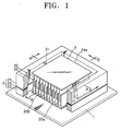
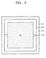
- a frame 2 in the shape of a rectangular border is situated on a base plate 1 that is made of Pyrex glass, etc. and a stage 3 is positioned inside the frame 2.
- the stage is supported by a torsion bar 31 that is connected to the frame 2 and extends to the middle part of two ends of the frame 2 which face each other.
- the frame 2, the stage 3, and the torsion bar 31 are formed integrally.
- the frame 2 and the torsion bar 31 provide an electrical path to the stage 3.
- the torsion bar 31 supports a see-saw motion of the stage 3, and provides an appropriate elastic restoring force upon movement of the stage.
- the frame 2 comprises a first frame layer 21 and a second frame layer 22 with a metal eutectic bonding layer plated with Au/Sn alloy between the two frame layer.
- the first frame layer 21, the stage 3, and the torsion bar 31 are obtained from a material plate, for example, a silicon wafer, that is made by a number of steps which will be described later. Between the first frame layer 21 and the stage 3 is a space 24a forming a rectangular separation border region.
- a plurality of driving comb-type electrodes 32 extend downward in a direction perpendicular to the bottom of the stage 3 and are parallel to one another.
- a plurality of fixed comb-type electrodes 34 that alternate between the driving comb-type electrodes 32 extend upward from the bottom of the stage 3.
- the fixed comb-type electrodes 34 are formed on first and second electrode bases 35a and 35b that are separated electrically.
- the fixed comb-type electrodes 34 formed on the first electrode base 35a generate a driving power for the stage 3 by the electrostatic force induced between the fixed comb-type electrodes 34 and the driving comb-type electrodes 32.
- the fixed comb-type electrodes 34 formed on the second electrode base 35b operate as a sensor of a variable capacitor, etc., depending on the relative position of the fixed and driving comb-type electrodes, together with the driving comb-type electrodes 32 on top corresponding to the fixed comb-type electrodes.
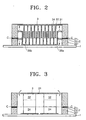
- the second frame layer 22 of the frame 2, the first and second electrode bases 35a and 35b, and the fixed comb-type electrodes 34 are made from a material plate, for example, a silicon wafer. Between the first and second electrodes 35a and 35b and the frame 2, a separation region 24b forming a rectangular border exists.
- the base plate 1 is an element that is attached as a separated piece when manufacturing the first and second electrode bases 35a and 35b and the second frame layer 22 of the frame 2.
- the first and second electrode bases 35a and 35b and the frame 2 and metal pads containing signal lines are formed thereon.
- the height of the fixed comb-type electrode is greater than that of the second frame layer 22.
- the front ends of the fixed comb-type electrodes 34 are positioned higher than the top of the second frame layer 22.
- the bottom ends (i.e., the front ends) of the driving comb-type electrodes 32 and the bottom of the first frame layer 21 are positioned on a common plane (C-C).
- the first and second frame layer easily bond the top and bottom structures made as separate plates.
- the driving comb-type electrodes 32 and the fixed comb-type electrodes 34 overlap with a certain width of space between them.
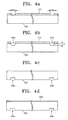
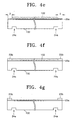
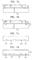
- FIGS. 4a through 4b illustrate one top structure.
- the process is carried out with a reinforcement wafer around 500 ⁇ m thick attached to the first plate 100, and the adhesive, for example, photoresist, that are used to bond the first plate 100 and the reinforcement wafer together is removed in this step. In doing so, each unit of the top structure is separated from the first plate 100. Each unit of the top structure is washed and dried, thus completing the top structure manufacture.
- the adhesive for example, photoresist
- the signal lines 203 shown in FIGS. 6a through 6d are illustrated schematically in order to facilitate understanding. In reality, there may be more signal lines produced than shown in the figures and they may be formed in a different pattern.
- the signal lines 203 shown in FIGS. 6a through 6d are connected to the first electrode base 35a and the second electrode base 35b and the frame(not shown). In FIGS. 1 through 3 the signal lines 203 are not shown.
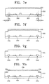
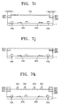
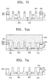
- FIGS. 7a through 7n illustrate one bottom structure.
- This step completes the manufacture of the micro-actuator by bonding the units of the top and bottom structures formed in the above processes.
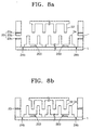
- top and bottom structures After aligning the top and bottom structures as shown in FIG 8a, they are bonded together into one structure as shown in FIG. 8b.
- the alignment and bonding of the top and bottom structures are realized with the aid of vacuum chucks.
- the top and bottom structures are individually bonded with a flip chip bonder.
- the two structures After fixing the top and bottom structures separately in two vacuum chucks, the two structures are aligned with the help of a microscope. When the arrangement is completed, the two vacuum chucks are drawn closer together, and the top and bottom structures are bonded into one structure.
- the metal eutectic bonding layer 23b melts and adheres to and the bottom metal layer 23c, thus the first frame layer 21 and second frame layer 22 of the frame 2 are joined into one structure.
- the metal layer 23 is shown as having a very thin thickness in FIG. 8b.
- the seed layer 23a, the metal eutectic bonding layer 23b and the bottom metal layer 23c, constituting the metal layer 23, are very thin and were shown exaggerated in the previous figures.
- the micro-actuator was manufactured using the processes described above. Driving the stage in a see-saw motion at a predetermined frequency and a certain angle range confirmed the expected results.
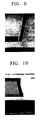
- FIGS. 9 and 10 are SEM photographs illustrating the top structure in the neighborhood of the torsion bar 31 in a micro-actuator manufactured according to the present invention.
- FIG. 11 is a SEM photograph illustrating the planar characteristic of the bottom structure.
- FIG. 12 is a magnified SEM photograph of the fixed comb-type electrode formed in the bottom structure.
- FIG. 13 is a magnified SEM photograph of the driving and fixed comb-type electrodes in the joined top and bottom structures, and
- FIG. 14 is a photograph illustrating the planar characteristic of a micro-actuator manufactured according to the present invention.
- the micro-actuator having the structure described above may be applied to various situations. If an optical mirror is formed on the surface of the stage, the micro-actuator may be used as an optical scanner that reflects incident light within a certain angular range. This optical scanner may be applied to the scanner of an optical head in an image display unit like televisions using laser and optical magnetic data storage units.
- the micro-actuator with the aimed structure can be made successfully, and may be produced particularly with a high manufacturing yield.
- foreign materials between comb-type electrodes that can be generated in the manufacturing process can be effectively prevented, and thus the top and bottom structures can be bonded quickly and reliably.
Landscapes
- Engineering & Computer Science (AREA)
- Microelectronics & Electronic Packaging (AREA)
- Manufacturing & Machinery (AREA)
- Micromachines (AREA)
Applications Claiming Priority (2)
| Application Number | Priority Date | Filing Date | Title |
|---|---|---|---|
| KR2000047809 | 2000-08-18 | ||
| KR10-2000-0047809A KR100400218B1 (ko) | 2000-08-18 | 2000-08-18 | 마이크로 액튜에이터 및 그 제조방법 |
Publications (3)
| Publication Number | Publication Date |
|---|---|
| EP1180493A2 true EP1180493A2 (fr) | 2002-02-20 |
| EP1180493A3 EP1180493A3 (fr) | 2003-01-08 |
| EP1180493B1 EP1180493B1 (fr) | 2006-08-02 |
Family
ID=36914999
Family Applications (1)
| Application Number | Title | Priority Date | Filing Date |
|---|---|---|---|
| EP01305088A Expired - Lifetime EP1180493B1 (fr) | 2000-08-18 | 2001-06-12 | Micro-actionneur et sa méthode de fabrication |
Country Status (5)
| Country | Link |
|---|---|
| US (2) | US6781279B2 (fr) |
| EP (1) | EP1180493B1 (fr) |
| JP (1) | JP2002137200A (fr) |
| KR (1) | KR100400218B1 (fr) |
| DE (1) | DE60121878T2 (fr) |
Cited By (12)
| Publication number | Priority date | Publication date | Assignee | Title |
|---|---|---|---|---|
| EP1203976A2 (fr) * | 2000-11-03 | 2002-05-08 | Samsung Electronics Co., Ltd. | Dispositif de balayage optique, projecteur à laser l'utilisant, et méthode d'opération du projecteur à laser |
| EP1344745A2 (fr) * | 2002-02-27 | 2003-09-17 | Samsung Electronics Co., Ltd. | Structure fabriquee par liaison anodique et son usage pour fabriquer un systeme de lecture optique |
| EP1508964A2 (fr) * | 2003-08-22 | 2005-02-23 | Samsung Electronics Co., Ltd. | Actionneur à deux axes de grandes dimensions |
| EP1526399A1 (fr) * | 2003-10-24 | 2005-04-27 | Samsung Electronics Co., Ltd. | Scanneur résonant réglable en fréquence |
| EP1659437A2 (fr) * | 2004-10-19 | 2006-05-24 | Samsung Electronics Co., Ltd. | Positionneur biaxial et son procédé de fabrication |
| WO2006114127A1 (fr) * | 2005-04-27 | 2006-11-02 | Micronic Laser Systems Ab | Dispositif mems comprenant une surface reflechissante et une surface d'electrode orientables perpendiculaires l'une a l'autre |
| WO2009074368A2 (fr) * | 2007-12-12 | 2009-06-18 | Robert Bosch Gmbh | Procédé de fabrication d'un composant micromécanique et composant micromécanique |
| CN103364120A (zh) * | 2012-04-10 | 2013-10-23 | 中国科学院电子学研究所 | 银锡共晶真空键合金属应变式mems压力传感器及其制造方法 |
| EP2066015A3 (fr) * | 2007-11-29 | 2014-06-25 | Stichting IMEC Nederland | Microstructure avec masse élargie et zone d'électrode pour conversion d'énergie cinétique en énergie électrique |
| WO2016015903A1 (fr) * | 2014-07-31 | 2016-02-04 | Robert Bosch Gmbh | Dispositif à micromiroirs, matrice de micromiroirs et dispositif de projection |
| WO2018015155A1 (fr) * | 2016-07-18 | 2018-01-25 | Carl Zeiss Smt Gmbh | Système capteur |
| WO2019172767A1 (fr) * | 2018-03-09 | 2019-09-12 | Scinvivo B.V. | Miroir de système microélectromécanique (mems) pour sonde oct et procédé de fabrication d'un tel miroir mems |
Families Citing this family (27)
| Publication number | Priority date | Publication date | Assignee | Title |
|---|---|---|---|---|
| KR100400218B1 (ko) * | 2000-08-18 | 2003-10-30 | 삼성전자주식회사 | 마이크로 액튜에이터 및 그 제조방법 |
| US6940636B2 (en) * | 2001-09-20 | 2005-09-06 | Analog Devices, Inc. | Optical switching apparatus and method of assembling same |
| US6893574B2 (en) * | 2001-10-23 | 2005-05-17 | Analog Devices Inc | MEMS capping method and apparatus |
| US6818532B2 (en) * | 2002-04-09 | 2004-11-16 | Oriol, Inc. | Method of etching substrates |
| JP4297049B2 (ja) | 2002-07-22 | 2009-07-15 | パナソニック株式会社 | 成分分離デバイスとその製造方法及びこれを用いた微小固形成分の分離方法 |
| US20040063237A1 (en) * | 2002-09-27 | 2004-04-01 | Chang-Han Yun | Fabricating complex micro-electromechanical systems using a dummy handling substrate |
| US6933163B2 (en) * | 2002-09-27 | 2005-08-23 | Analog Devices, Inc. | Fabricating integrated micro-electromechanical systems using an intermediate electrode layer |
| US6964882B2 (en) | 2002-09-27 | 2005-11-15 | Analog Devices, Inc. | Fabricating complex micro-electromechanical systems using a flip bonding technique |
| KR100486716B1 (ko) * | 2002-10-18 | 2005-05-03 | 삼성전자주식회사 | 2-d 액튜에이터 및 그 제조방법 |
| JP4337511B2 (ja) * | 2003-02-12 | 2009-09-30 | 株式会社デンソー | 静電アクチュエータおよびその製造方法 |
| US7688689B2 (en) * | 2004-02-26 | 2010-03-30 | Seagate Technology Llc | Head with optical bench for use in data storage devices |
| US7099063B2 (en) * | 2004-03-09 | 2006-08-29 | Lucent Technologies Inc. | MEMS device for an adaptive optics mirror |
| CN100339738C (zh) * | 2004-03-12 | 2007-09-26 | 先进微系统科技股份有限公司 | 具有多组梳状电极的微机电致动器及其制造方法 |
| US7068409B2 (en) * | 2004-03-31 | 2006-06-27 | Lucent Technologies Inc. | Tip-tilt-piston actuator |
| JP2006149140A (ja) * | 2004-11-24 | 2006-06-08 | Alps Electric Co Ltd | 静電吸引駆動装置 |
| US7583006B2 (en) * | 2005-07-26 | 2009-09-01 | Siimpel Corporation | MEMS digital linear actuator |
| FR2889371A1 (fr) * | 2005-07-29 | 2007-02-02 | Commissariat Energie Atomique | Dispositif de conversion de l'energie mecanique en energie electrique par cycle de charges et de decharges electriques sur les peignes d'un condensateur |
| JP4621577B2 (ja) * | 2005-10-27 | 2011-01-26 | アルプス電気株式会社 | 静電アクチュエータ及びその駆動方法 |
| JP4616156B2 (ja) * | 2005-11-18 | 2011-01-19 | アルプス電気株式会社 | 静電アクチュエータ |
| WO2008114330A1 (fr) * | 2007-02-19 | 2008-09-25 | Fujitsu Limited | Dispositif mems et commutateur optique |
| US7412892B1 (en) | 2007-06-06 | 2008-08-19 | Measurement Specialties, Inc. | Method of making pressure transducer and apparatus |
| US8085508B2 (en) | 2008-03-28 | 2011-12-27 | Hitachi Global Storage Technologies Netherlands B.V. | System, method and apparatus for flexure-integrated microactuator |
| US8609450B2 (en) * | 2010-12-06 | 2013-12-17 | International Business Machines Corporation | MEMS switches and fabrication methods |
| DE102013212095B4 (de) * | 2013-06-25 | 2024-06-27 | Robert Bosch Gmbh | Mikro-elektromechanischer Reflektor und Verfahren zum Herstellen eines mikro-elektromechanischen Reflektors |
| KR20160140698A (ko) | 2014-04-04 | 2016-12-07 | 멤스 스타트 엘엘씨 | 광전자 소자를 이동시키기 위한 액추에이터 |
| CN106132867B (zh) * | 2014-04-04 | 2019-02-15 | Mems启动有限公司 | 用于移动光电设备的致动器 |
| CN115893309A (zh) * | 2021-08-20 | 2023-04-04 | 华为技术有限公司 | 制造微机电系统梳齿结构的方法、系统和梳齿结构 |
Citations (7)
| Publication number | Priority date | Publication date | Assignee | Title |
|---|---|---|---|---|
| JPH05302182A (ja) * | 1992-02-25 | 1993-11-16 | Fuji Electric Co Ltd | 櫛歯式アクチュエータの製造方法 |
| US5668033A (en) * | 1995-05-18 | 1997-09-16 | Nippondenso Co., Ltd. | Method for manufacturing a semiconductor acceleration sensor device |
| DE19744292A1 (de) * | 1996-10-07 | 1998-04-23 | Inst Mikro Und Informationstec | Elektrostatischer Aktor und Sensor |
| US5999306A (en) * | 1995-12-01 | 1999-12-07 | Seiko Epson Corporation | Method of manufacturing spatial light modulator and electronic device employing it |
| JP2000011556A (ja) * | 1998-06-16 | 2000-01-14 | Alps Electric Co Ltd | マイクロアクチュエータ及び磁気ヘッド装置並びに磁気記録装置 |
| JP2000147419A (ja) * | 1998-11-13 | 2000-05-26 | Victor Co Of Japan Ltd | 光偏向器及びこれを用いた表示装置 |
| EP1020984A2 (fr) * | 1999-01-11 | 2000-07-19 | Samsung Electronics Co., Ltd. | Une structure de peine tridimensionnelle |
Family Cites Families (16)
| Publication number | Priority date | Publication date | Assignee | Title |
|---|---|---|---|---|
| US5025346A (en) * | 1989-02-17 | 1991-06-18 | Regents Of The University Of California | Laterally driven resonant microstructures |
| JP2647194B2 (ja) * | 1989-04-17 | 1997-08-27 | 住友電気工業株式会社 | 半導体用パッケージの封止方法 |
| US5097480A (en) * | 1990-01-24 | 1992-03-17 | The Mitre Corporation | Acoustic modulation apparatus for laser |
| JP3006178B2 (ja) * | 1991-06-21 | 2000-02-07 | 富士電機株式会社 | 静電式アクチュエータ |
| US5536988A (en) * | 1993-06-01 | 1996-07-16 | Cornell Research Foundation, Inc. | Compound stage MEM actuator suspended for multidimensional motion |
| US5629790A (en) * | 1993-10-18 | 1997-05-13 | Neukermans; Armand P. | Micromachined torsional scanner |
| US6116863A (en) * | 1997-05-30 | 2000-09-12 | University Of Cincinnati | Electromagnetically driven microactuated device and method of making the same |
| KR100217085B1 (ko) | 1997-08-30 | 1999-09-01 | 정몽규 | 전자제어장치의 안정성 검사장치 |
| US6062461A (en) * | 1998-06-03 | 2000-05-16 | Delphi Technologies, Inc. | Process for bonding micromachined wafers using solder |
| US6116853A (en) * | 1998-11-13 | 2000-09-12 | Siemens Aktiengesellschaft | Method and apparatus for checking the operating reliability of a turbine during load shedding |
| JP3993343B2 (ja) * | 1999-06-29 | 2007-10-17 | 富士通株式会社 | ガルバノマイクロミラー |
| US6262463B1 (en) * | 1999-07-08 | 2001-07-17 | Integrated Micromachines, Inc. | Micromachined acceleration activated mechanical switch and electromagnetic sensor |
| EP1240708A2 (fr) * | 1999-11-29 | 2002-09-18 | Iolon, Inc. | Micro-dispositif equilibre et microactionneur electrostatique rotatif s'utilisant avec ce micro-dispositif |
| KR100400218B1 (ko) * | 2000-08-18 | 2003-10-30 | 삼성전자주식회사 | 마이크로 액튜에이터 및 그 제조방법 |
| JP2002148554A (ja) * | 2000-11-03 | 2002-05-22 | Samsung Electronics Co Ltd | 光スキャナ及びこれを適用したレーザ映像投射装置並びにその駆動方法 |
| KR100396551B1 (ko) * | 2001-02-03 | 2003-09-03 | 삼성전자주식회사 | 웨이퍼 레벨 허메틱 실링 방법 |
-
2000
- 2000-08-18 KR KR10-2000-0047809A patent/KR100400218B1/ko not_active IP Right Cessation
-
2001
- 2001-06-05 US US09/873,382 patent/US6781279B2/en not_active Expired - Fee Related
- 2001-06-12 EP EP01305088A patent/EP1180493B1/fr not_active Expired - Lifetime
- 2001-06-12 DE DE60121878T patent/DE60121878T2/de not_active Expired - Fee Related
- 2001-08-10 JP JP2001243828A patent/JP2002137200A/ja not_active Withdrawn
-
2004
- 2004-03-04 US US10/791,756 patent/US7083737B2/en not_active Expired - Fee Related
Patent Citations (7)
| Publication number | Priority date | Publication date | Assignee | Title |
|---|---|---|---|---|
| JPH05302182A (ja) * | 1992-02-25 | 1993-11-16 | Fuji Electric Co Ltd | 櫛歯式アクチュエータの製造方法 |
| US5668033A (en) * | 1995-05-18 | 1997-09-16 | Nippondenso Co., Ltd. | Method for manufacturing a semiconductor acceleration sensor device |
| US5999306A (en) * | 1995-12-01 | 1999-12-07 | Seiko Epson Corporation | Method of manufacturing spatial light modulator and electronic device employing it |
| DE19744292A1 (de) * | 1996-10-07 | 1998-04-23 | Inst Mikro Und Informationstec | Elektrostatischer Aktor und Sensor |
| JP2000011556A (ja) * | 1998-06-16 | 2000-01-14 | Alps Electric Co Ltd | マイクロアクチュエータ及び磁気ヘッド装置並びに磁気記録装置 |
| JP2000147419A (ja) * | 1998-11-13 | 2000-05-26 | Victor Co Of Japan Ltd | 光偏向器及びこれを用いた表示装置 |
| EP1020984A2 (fr) * | 1999-01-11 | 2000-07-19 | Samsung Electronics Co., Ltd. | Une structure de peine tridimensionnelle |
Non-Patent Citations (3)
| Title |
|---|
| INDERMUEHLE P-F ET AL: "DESIGN AND FABRICATION OF AN OVERHANGING XY-MICROACTUATOR WITH INTEGRATED TIP FOR SCANNING SURFACE PROFILING" SENSORS AND ACTUATORS A, ELSEVIER SEQUOIA S.A., LAUSANNE, CH, vol. A43, no. 1/3, 1 May 1994 (1994-05-01), pages 346-350, XP000454132 ISSN: 0924-4247 * |
| PATENT ABSTRACTS OF JAPAN vol. 018, no. 107 (C-1169), 22 February 1994 (1994-02-22) -& JP 05 302182 A (FUJI ELECTRIC CO LTD), 16 November 1993 (1993-11-16) * |
| PATENT ABSTRACTS OF JAPAN vol. 2000, no. 04, 31 August 2000 (2000-08-31) -& JP 2000 011556 A (ALPS ELECTRIC CO LTD;ESASHI MASAKI), 14 January 2000 (2000-01-14) -& US 6 424 504 B1 (M ABE ET AL) 23 July 2002 (2002-07-23) * |
Cited By (22)
| Publication number | Priority date | Publication date | Assignee | Title |
|---|---|---|---|---|
| EP1203976A3 (fr) * | 2000-11-03 | 2004-03-24 | Samsung Electronics Co., Ltd. | Dispositif de balayage optique, projecteur à laser l'utilisant, et méthode d'opération du projecteur à laser |
| EP1203976A2 (fr) * | 2000-11-03 | 2002-05-08 | Samsung Electronics Co., Ltd. | Dispositif de balayage optique, projecteur à laser l'utilisant, et méthode d'opération du projecteur à laser |
| US7255768B2 (en) | 2002-02-27 | 2007-08-14 | Samsung Electronics Co., Ltd. | Anodic bonding structure, fabricating method thereof, and method of manufacturing optical scanner using the same |
| EP1344745A2 (fr) * | 2002-02-27 | 2003-09-17 | Samsung Electronics Co., Ltd. | Structure fabriquee par liaison anodique et son usage pour fabriquer un systeme de lecture optique |
| EP1344745A3 (fr) * | 2002-02-27 | 2005-01-12 | Samsung Electronics Co., Ltd. | Structure fabriquee par liaison anodique et son usage pour fabriquer un systeme de lecture optique |
| EP1508964A2 (fr) * | 2003-08-22 | 2005-02-23 | Samsung Electronics Co., Ltd. | Actionneur à deux axes de grandes dimensions |
| EP1508964A3 (fr) * | 2003-08-22 | 2005-10-19 | Samsung Electronics Co., Ltd. | Actionneur à deux axes de grandes dimensions |
| EP1526399A1 (fr) * | 2003-10-24 | 2005-04-27 | Samsung Electronics Co., Ltd. | Scanneur résonant réglable en fréquence |
| US7242511B2 (en) | 2003-10-24 | 2007-07-10 | Samsung Electronics Co., Ltd. | Frequency tunable resonant scanner |
| US7436574B2 (en) | 2003-10-24 | 2008-10-14 | Samsung Electronics Co., Ltd. | Frequency tunable resonant scanner |
| EP1659437A2 (fr) * | 2004-10-19 | 2006-05-24 | Samsung Electronics Co., Ltd. | Positionneur biaxial et son procédé de fabrication |
| EP1659437A3 (fr) * | 2004-10-19 | 2009-06-17 | Samsung Electronics Co., Ltd. | Positionneur biaxial et son procédé de fabrication |
| WO2006114127A1 (fr) * | 2005-04-27 | 2006-11-02 | Micronic Laser Systems Ab | Dispositif mems comprenant une surface reflechissante et une surface d'electrode orientables perpendiculaires l'une a l'autre |
| EP2066015A3 (fr) * | 2007-11-29 | 2014-06-25 | Stichting IMEC Nederland | Microstructure avec masse élargie et zone d'électrode pour conversion d'énergie cinétique en énergie électrique |
| WO2009074368A3 (fr) * | 2007-12-12 | 2009-11-12 | Robert Bosch Gmbh | Procédé de fabrication d'un composant micromécanique et composant micromécanique |
| WO2009074368A2 (fr) * | 2007-12-12 | 2009-06-18 | Robert Bosch Gmbh | Procédé de fabrication d'un composant micromécanique et composant micromécanique |
| CN103364120A (zh) * | 2012-04-10 | 2013-10-23 | 中国科学院电子学研究所 | 银锡共晶真空键合金属应变式mems压力传感器及其制造方法 |
| WO2016015903A1 (fr) * | 2014-07-31 | 2016-02-04 | Robert Bosch Gmbh | Dispositif à micromiroirs, matrice de micromiroirs et dispositif de projection |
| WO2018015155A1 (fr) * | 2016-07-18 | 2018-01-25 | Carl Zeiss Smt Gmbh | Système capteur |
| US10514276B2 (en) | 2016-07-18 | 2019-12-24 | Carl Zeiss Smt Gmbh | Sensor device |
| WO2019172767A1 (fr) * | 2018-03-09 | 2019-09-12 | Scinvivo B.V. | Miroir de système microélectromécanique (mems) pour sonde oct et procédé de fabrication d'un tel miroir mems |
| US12066620B2 (en) | 2018-03-09 | 2024-08-20 | Scinvivo B.V. | MEMS mirror for OCT probe and method of manufacturing such MEMS mirror |
Also Published As
| Publication number | Publication date |
|---|---|
| DE60121878D1 (de) | 2006-09-14 |
| KR100400218B1 (ko) | 2003-10-30 |
| US20040163226A1 (en) | 2004-08-26 |
| US7083737B2 (en) | 2006-08-01 |
| KR20020014486A (ko) | 2002-02-25 |
| EP1180493A3 (fr) | 2003-01-08 |
| DE60121878T2 (de) | 2007-03-08 |
| US6781279B2 (en) | 2004-08-24 |
| JP2002137200A (ja) | 2002-05-14 |
| EP1180493B1 (fr) | 2006-08-02 |
| US20020021055A1 (en) | 2002-02-21 |
Similar Documents
| Publication | Publication Date | Title |
|---|---|---|
| EP1180493B1 (fr) | Micro-actionneur et sa méthode de fabrication | |
| JP4142919B2 (ja) | 光スキャナおよびその製造方法 | |
| US6995495B2 (en) | 2-D actuator and manufacturing method thereof | |
| US8043513B2 (en) | Gimbal-less micro-electro-mechanical-system tip-tilt and tip-tilt-piston actuators and a method for forming the same | |
| US8462410B2 (en) | Mirror device, mirror array, optical switch, mirror device manufacturing method, and mirror substrate manufacturing method | |
| US6989921B2 (en) | Magnetically actuated micro-electro-mechanical apparatus and method of manufacture | |
| EP1918758A2 (fr) | Micro-actionneur électromagnétique | |
| US7719163B2 (en) | Actuator having fixed and movable comb electrodes | |
| US8790936B2 (en) | Method for manufacturing optical deflector for forming dicing street with double etching | |
| US7623283B2 (en) | Actuator | |
| US7203393B2 (en) | MEMS micro mirrors driven by electrodes fabricated on another substrate | |
| CN111983801A (zh) | 用于补偿不期望的运动的压电mems致动器及其制造工艺 | |
| US20060166444A1 (en) | MEMS scanning mirror with trenched surface and i-beam like cross-section for reducing inertia and deformation | |
| JP7105934B2 (ja) | Memsミラー装置及びその製造方法 | |
| JP2007121464A (ja) | チルトミラー素子及びその駆動方法 | |
| CA2355450A1 (fr) | Miroirs a fixations hybrides pour commutateur optique de systeme microelectromecanique | |
| JP2001235703A (ja) | アクチュエータ |
Legal Events
| Date | Code | Title | Description |
|---|---|---|---|
| PUAI | Public reference made under article 153(3) epc to a published international application that has entered the european phase |
Free format text: ORIGINAL CODE: 0009012 |
|
| AK | Designated contracting states |
Kind code of ref document: A2 Designated state(s): AT BE CH CY DE DK ES FI FR GB GR IE IT LI LU MC NL PT SE TR |
|
| AX | Request for extension of the european patent |
Free format text: AL;LT;LV;MK;RO;SI |
|
| PUAL | Search report despatched |
Free format text: ORIGINAL CODE: 0009013 |
|
| AK | Designated contracting states |
Kind code of ref document: A3 Designated state(s): AT BE CH CY DE DK ES FI FR GB GR IE IT LI LU MC NL PT SE TR |
|
| AX | Request for extension of the european patent |
Free format text: AL;LT;LV;MK;RO;SI |
|
| 17P | Request for examination filed |
Effective date: 20030611 |
|
| AKX | Designation fees paid |
Designated state(s): CH DE FR GB LI NL |
|
| 17Q | First examination report despatched |
Effective date: 20040615 |
|
| GRAP | Despatch of communication of intention to grant a patent |
Free format text: ORIGINAL CODE: EPIDOSNIGR1 |
|
| GRAS | Grant fee paid |
Free format text: ORIGINAL CODE: EPIDOSNIGR3 |
|
| GRAA | (expected) grant |
Free format text: ORIGINAL CODE: 0009210 |
|
| AK | Designated contracting states |
Kind code of ref document: B1 Designated state(s): CH DE FR GB LI NL |
|
| PG25 | Lapsed in a contracting state [announced via postgrant information from national office to epo] |
Ref country code: CH Free format text: LAPSE BECAUSE OF FAILURE TO SUBMIT A TRANSLATION OF THE DESCRIPTION OR TO PAY THE FEE WITHIN THE PRESCRIBED TIME-LIMIT Effective date: 20060802 Ref country code: LI Free format text: LAPSE BECAUSE OF FAILURE TO SUBMIT A TRANSLATION OF THE DESCRIPTION OR TO PAY THE FEE WITHIN THE PRESCRIBED TIME-LIMIT Effective date: 20060802 |
|
| REG | Reference to a national code |
Ref country code: GB Ref legal event code: FG4D |
|
| REG | Reference to a national code |
Ref country code: CH Ref legal event code: EP |
|
| REF | Corresponds to: |
Ref document number: 60121878 Country of ref document: DE Date of ref document: 20060914 Kind code of ref document: P |
|
| REG | Reference to a national code |
Ref country code: CH Ref legal event code: PL |
|
| ET | Fr: translation filed | ||
| PLBE | No opposition filed within time limit |
Free format text: ORIGINAL CODE: 0009261 |
|
| STAA | Information on the status of an ep patent application or granted ep patent |
Free format text: STATUS: NO OPPOSITION FILED WITHIN TIME LIMIT |
|
| 26N | No opposition filed |
Effective date: 20070503 |
|
| PGFP | Annual fee paid to national office [announced via postgrant information from national office to epo] |
Ref country code: NL Payment date: 20090603 Year of fee payment: 9 |
|
| PGFP | Annual fee paid to national office [announced via postgrant information from national office to epo] |
Ref country code: DE Payment date: 20090604 Year of fee payment: 9 Ref country code: GB Payment date: 20090610 Year of fee payment: 9 |
|
| REG | Reference to a national code |
Ref country code: NL Ref legal event code: V1 Effective date: 20110101 |
|
| GBPC | Gb: european patent ceased through non-payment of renewal fee |
Effective date: 20100612 |
|
| REG | Reference to a national code |
Ref country code: FR Ref legal event code: ST Effective date: 20110228 |
|
| PG25 | Lapsed in a contracting state [announced via postgrant information from national office to epo] |
Ref country code: DE Free format text: LAPSE BECAUSE OF NON-PAYMENT OF DUE FEES Effective date: 20110101 |
|
| PG25 | Lapsed in a contracting state [announced via postgrant information from national office to epo] |
Ref country code: FR Free format text: LAPSE BECAUSE OF NON-PAYMENT OF DUE FEES Effective date: 20100630 Ref country code: NL Free format text: LAPSE BECAUSE OF NON-PAYMENT OF DUE FEES Effective date: 20110101 |
|
| PG25 | Lapsed in a contracting state [announced via postgrant information from national office to epo] |
Ref country code: GB Free format text: LAPSE BECAUSE OF NON-PAYMENT OF DUE FEES Effective date: 20100612 |
|
| PGFP | Annual fee paid to national office [announced via postgrant information from national office to epo] |
Ref country code: FR Payment date: 20090611 Year of fee payment: 9 |