EP1168359B1 - Vefahren zur Steurung eines Lesezugriffs auf einen dynamischen Speicher und Speicher dazu - Google Patents
Vefahren zur Steurung eines Lesezugriffs auf einen dynamischen Speicher und Speicher dazu Download PDFInfo
- Publication number
- EP1168359B1 EP1168359B1 EP01401558A EP01401558A EP1168359B1 EP 1168359 B1 EP1168359 B1 EP 1168359B1 EP 01401558 A EP01401558 A EP 01401558A EP 01401558 A EP01401558 A EP 01401558A EP 1168359 B1 EP1168359 B1 EP 1168359B1
- Authority
- EP
- European Patent Office
- Prior art keywords
- bit line
- memory
- voltage
- charging
- read
- Prior art date
- Legal status (The legal status is an assumption and is not a legal conclusion. Google has not performed a legal analysis and makes no representation as to the accuracy of the status listed.)
- Expired - Lifetime
Links
- 230000015654 memory Effects 0.000 title claims description 60
- 238000000034 method Methods 0.000 title claims description 8
- 239000003990 capacitor Substances 0.000 claims description 35
- 230000008569 process Effects 0.000 claims description 3
- 230000036316 preload Effects 0.000 description 11
- 238000005516 engineering process Methods 0.000 description 10
- 230000003213 activating effect Effects 0.000 description 5
- 230000004913 activation Effects 0.000 description 5
- 230000009849 deactivation Effects 0.000 description 3
- 238000001465 metallisation Methods 0.000 description 3
- 230000003071 parasitic effect Effects 0.000 description 2
- 240000008042 Zea mays Species 0.000 description 1
- 230000000295 complement effect Effects 0.000 description 1
- 238000001816 cooling Methods 0.000 description 1
- 230000007423 decrease Effects 0.000 description 1
- 238000001514 detection method Methods 0.000 description 1
- 238000010586 diagram Methods 0.000 description 1
- 230000000694 effects Effects 0.000 description 1
- 230000004048 modification Effects 0.000 description 1
- 238000012986 modification Methods 0.000 description 1
- 230000000737 periodic effect Effects 0.000 description 1
- 230000002035 prolonged effect Effects 0.000 description 1
- 230000001902 propagating effect Effects 0.000 description 1
- 230000003068 static effect Effects 0.000 description 1
Images


Classifications
-
- G—PHYSICS
- G11—INFORMATION STORAGE
- G11C—STATIC STORES
- G11C11/00—Digital stores characterised by the use of particular electric or magnetic storage elements; Storage elements therefor
- G11C11/21—Digital stores characterised by the use of particular electric or magnetic storage elements; Storage elements therefor using electric elements
- G11C11/34—Digital stores characterised by the use of particular electric or magnetic storage elements; Storage elements therefor using electric elements using semiconductor devices
- G11C11/40—Digital stores characterised by the use of particular electric or magnetic storage elements; Storage elements therefor using electric elements using semiconductor devices using transistors
- G11C11/401—Digital stores characterised by the use of particular electric or magnetic storage elements; Storage elements therefor using electric elements using semiconductor devices using transistors forming cells needing refreshing or charge regeneration, i.e. dynamic cells
- G11C11/4063—Auxiliary circuits, e.g. for addressing, decoding, driving, writing, sensing or timing
- G11C11/407—Auxiliary circuits, e.g. for addressing, decoding, driving, writing, sensing or timing for memory cells of the field-effect type
- G11C11/409—Read-write [R-W] circuits
- G11C11/4094—Bit-line management or control circuits
Definitions
- the invention relates to dynamic random access memories (DRAM: "Dynamic Random Access Memory” in English), and in particular the command of a read access and more particularly the control of the operation of the read / rewrite amplifiers.
- DRAM dynamic random access memories
- the invention applies advantageously but not limited to dynamic memories called "on-board” ("embedded DRAM” in English), i.e. memories which are for example produced jointly with other components by a same technological process, and intended to be integrated together within a specific integrated circuit (ASIC).
- on-board embedded DRAM
- ASIC specific integrated circuit
- the dynamic memories As opposed to static random access memory (SRAM), in which the stored information remains at least indefinitely as long as this memory remains supplied, the dynamic memories have the peculiarity of requiring a periodic refreshment of the information stored due in particular to parasitic leakage currents which offload the storage capacity of each memory point.
- SRAM static random access memory
- dynamic random access memory cells we can in particular quote those comprising one, two or three transistors.
- bit line bit line in language English
- bit line reference bit line not
- Means are also provided for column preload to preload the bit line and bit line of reference of the column before a read access of the memory.
- the bit lines and reference bit lines are preloaded generally at a voltage equal to Vdd / 2 in the case where the voltage supply voltage Vdd represents the memory voltage for a high state (typically a logical "1") and 0 volts (ground) represents the voltage of storage of a low state (typically a logical "0").
- DRAM memories use a row of cells so-called “reference”, also connected on the bit lines and reference bit lines, to equalize the loads of bit lines and reference bit lines and maximize average signal amplitude between "0" and "1".
- Preloading Reference cells are also generally performed at Vdd / 2.
- This amplifier usually has two looped reversers (forming a bistable rocker), each formed of two complementary transistors controlled by two signals successive read and rewrite (commonly known as respectively "sense” and "restore” in English).
- the voltage at the gates of the two NMOS transistors of the amplifier read / rewrite is approximately Vdd / 2.
- the source of these two NMOS transistors is then brought to ground.
- the gate-source voltage of these NMOS transistors is then substantially equal to Vdd / 2. Now, these transistors are on if the gate-source voltage is greater than the threshold voltage of these transistors.
- the level of tension power supply drops, while the threshold voltage of an NMOS transistor remains substantially constant. So for 0.18 micron technology, the supply voltage is around 1.8 volts, while for a 0.12 micron technology, it is around 1.2 volts.
- the invention aims to provide a solution to this problem.
- the invention aims to guarantee the proper functioning of the read / rewrite amplifier, especially for technologies advanced technologies such as 0.15 or 0.12 micron or less.
- the invention therefore provides a method for controlling access by reading of a memory cell from a memory plan of a dynamic random access memory, said memory cell being connected to a bit line of the memory plane and associated with an amplifier read / rewrite connected between the bit line and a bit line of reference.
- the control method includes a phase of precharging the bit line and the reference bit line at a precharge voltage predetermined (for example Vdd / 2) and a reading and refresh the contents of the memory cell in which select the memory cell and activate the amplifier read / rewrite.
- a precharge voltage predetermined for example Vdd / 2
- the common mode voltage of the read / rewrite amplifier so as to increase the voltage on the grid of the NMOS transistors and therefore obtain a difference of higher gate-source voltage across the NMOS transistors, even with a lower supply voltage.
- charging is each capacitor for a predetermined time, for example during the precharge time of the bit lines and bit lines of reference, and we stop the charge just before connecting the capacitor thus loaded to the corresponding bit line. Stopping the charge just before connecting the capacitor to the corresponding bit line, thus minimizes parasitic leaks.
- the means of control are able to activate the charging means for a period predetermined, then deactivate the charging means just before close the two connection switches.
- the charging means advantageously comprise for each capacitor, a controllable charge switch connected between a voltage source delivering said charge voltage (for example the supply voltage), and a capacitor terminal.
- the reference DMV generally designates a RAM device according to the invention.
- This memory device also includes a memory plan with CM memory cells organized in rows and columns.
- Each memory cell CM is here a memory cell comprising an access transistor TA and a storage capacitor CC.
- the invention is not limited to this type of memory cell lively dynamic.
- CM cells in the same row can be simultaneously activated by a WL activation signal propagating on a line of words ("word line" in English). Indeed, the grids of transistor TA of these memory cells CM are connected to this line of word WL. In addition, all the cells in the row are respectively connected to metallizations of BL column or bit line.
- Each bit line BL is also associated with a line of immediately adjacent bit BLN, commonly called by man of the profession bit line reference (or "bit line not” in English). These BLN bit lines allow other rows to be staggered of memory cells. Of course, for a connected memory cell on a BLN bit line, the BL bit line then acts as a bit line reference.
- a DCD column decoder is provided at the foot of each column. of conventional structure and known per se, controlled by a signal Cmd column decoding. This DCD column decoder allows select one of the columns of the memory plan to allow the delivery to the I / O output interface of the RAM device, contents of the memory cell placed at the intersection of the column selected and from the selected row.
- the DMV RAM device also includes controllable means of MPCH column preload, of structure classic and known per se.
- MPCH means are for example formed here by three transistors controlled by the PCH signal.
- These means of preload here are actually means of "pinching" the bit line BL and the BLN reference bit line of a column, and allow when pinch, that is to say when the three transistors are on, equalize the potential of the bit line and the reference bit line.
- All MPCH precharge means of the memory device live can be connected to a generator (not shown here for purposes simplification) which makes it possible to maintain the precharge voltages of the bit lines and reference bit lines in the case for example prolonged memory inactivity, in order to limit the effects of current leakage.
- the DMV RAM device also includes classic way, a controllable read / rewrite amplifier AMLE connected on each column of the memory plan. More precisely, this read / rewrite amplifier is connected between the bit line BL and the reference bit line BLN of the column.
- the structure of such read / rewrite amplifier is known to a person skilled in the art, in particular by French patent application No. 2,768,847.
- FIG. 2 in schematically illustrates the essential aspects.
- the AMLE amplifier has two amplifiers looped back, formed by two PMOS transistors referenced TP1 and TP2, and two NMOS transistors referenced TN1 and TN2.
- the S sources of these two NMOS transistors are connected to ground via a TSN control transistor controlled on its gate by a signal SN reading ("sense" signal).
- the sources of the two transistors PMOS TP1 and TP2 are connected to the supply voltage Vdd by via another TRS control transistor controlled on its grid by an RS (“restore”) rewrite signal.
- the grids of the transistors TN1 and TN2 in particular, are connected crosswise to the bit line BL and the reference bit line BLN.
- the device for DMV RAM includes MCM means connected on the bit line BL and on the reference bit line BLN of each column and intended, as will be seen in more detail below, for boost the common mode voltage of the AMLE amplifier.
- the activation signal WL conveyed by the metallization carrying the same reference, as well as the SN, RS, Cmd, PCH control signals, WLB, WLP, are delivered by CTL control means which can be conventionally made based on logic gate.
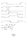
- FIG. 3 We now refer more particularly to FIG. 3, for describe an embodiment of the method according to the invention.
- VCC across the DC memory capacity of the memory cell is equal to Vdd (neglecting the leakage currents).
- Vbl cbl 2. (Cbl + Ccell) + Ccell (Cbl + Ccell) ].
- the voltage Vbl is equal to 0.615 Vdd.
- the VCC voltage balances with the voltage of the bit line BL at an intermediate value between Vbl and Vdd, while the voltage of the reference bit line BLN decreases slightly.
- the SN signal is then activated, which allows the data to be read. contained in the memory cell, then we activate the RS signal, which allows to rewrite this data in the memory cell, and by Therefore to refresh it.
- Activation of the RS signal has conventionally for consequence of raising the tension of the line of bit BL and the voltage VCC at the supply voltage and to drop the BLN bit line voltage at 0.
- the read and refresh cycle ends with the deactivation of the WL signal, then deactivation of the SN and RS signals.
- the WLP signal which in this case was reactivated after the WLB signal deactivation, can be done at any time before the activation of the WLB signal and in particular concomitantly with the preload bit lines and reference bit lines.
- the invention thus makes it very simple to increase the common mode of the read / rewrite amplifier.
- This modification which consists of adding capacitors and transistors, does not consume any energy other than that necessary for charge the capacitors.
Landscapes
- Engineering & Computer Science (AREA)
- Microelectronics & Electronic Packaging (AREA)
- Computer Hardware Design (AREA)
- Dram (AREA)
Claims (5)
- Verfahren zur Steuerung eines Lesezugriffs auf eine Speicherzelle einer Speicherebene einer dynamischen Speichervorrichtung, wobei die Speicherzelle (CM) mit einer Bitleitung (BL) der Speicherebene verbunden ist und an einem Lese/Überschreib-Verstärker (AMLE) angeschlossen ist, der zwischen der Bitleitung und einer Referenzbitleitung (BLN) angeordnet ist, mit einer Phase des Voraufladens der Bitleitung und der Referenzbitleitung auf eine vorgegebene Voraufladespannung und einer Lese- und Auffrischungsphase des Inhalts der Speicherzelle, in welcher die Speicherzelle gewählt wird und der Lese/Überschreib-Verstärker aktiviert wird, dadurch gekennzeichnet, daß zwischen der Voraufladephase und der Lese- und Auffrischungsphase zwei Kondensatoren (DCC) mit der Bitleitung bzw. mit der Referenzbitleitung verbunden werden, die zuvor mit einer Aufladespannung (Vdd) aufgeladen wurden, die höher als die Voraufladespannung (Vdd/2) ist.
- Verfahren nach Anspruch 1, dadurch gekennzeichnet, daß jeder Kondensator (DCC) während einer vorgegebenen Dauer aufgeladen wird und das Aufladen beendet wird, unmittelbar bevor der auf diese Weise aufgeladene Kondensator mit der entsprechenden Bitleitung verbunden wird.
- Dynamische Speichervorrichtung mit:dadurch gekennzeichnet, daß sie ferner aufweist:einer Speicherebene, die Spalten aufweist, die jeweils mit einer Bitleitung (BL) und einer Referenzbitleitung (BLN) gebildet sind, an welchen Speicherzellenreihen angeschlossen sind,einem steuerbaren Lese/Überschreib-Verstärker (AMLE), der mit jeder Spalte der Speicherebene verbunden ist,einer steuerbaren Einrichtung zum Auswählen einer Speicherzellenreihe,eine steuerbare Spaltenvoraufladeeinrichtung (MPCH), die mit jeder Spalte verbunden ist, um die Bitleitung und die Referenzbitleitung der Spalte auf eine vorgegebene Voraufladespannung aufzuladen,zwei Kondensatoren (DCC), die über zwei steuerbare Verbindungsunterbrecher (T2) mit der Bitleitung bzw. der Referenzbitleitung einer Spalte verbunden sind,eine steuerbare Aufladevorrichtung (T1, Vdd), die jeden Kondensator auf eine Aufladespannung aufladen kann, die höher als die Voraufladespannung ist,eine Steuerungseinrichtung (CTL), die fähig ist, die Kondensatoraufladeeinrichtung zu aktivieren und der Reihe nach die Voraufladeeinrichtung, die zwei Verbindungsunterbrecher, die Auswahleinrichtung und den Lese/Überschreib-Verstärker zu aktivieren.
- Vorrichtung nach Anspruch 3, dadurch gekennzeichnet, daß die Steuerungseinrichtung fähig ist, die Aufladeeinrichtung während einer vorgegebenen Zeitdauer zu aktivieren, die Aufladeeinrichtung dann zu deaktivieren, unmittelbar bevor die zwei Verbindungsunterbrecher (T2) geschlossen werden.
- Vorrichtung nach Anspruch 3 oder 4, dadurch gekennzeichnet, daß die Aufladeeinrichtung für jeden Kondensator (DCC) einen steuerbaren Aufladeunterbrecher (T1) aufweist, der zwischen einer Spannungsquelle, die die Aufladespannung (Vdd) liefert, und einer Klemme des Kondensators (DCC) angeschlossen ist.
Applications Claiming Priority (2)
| Application Number | Priority Date | Filing Date | Title |
|---|---|---|---|
| FR0008131 | 2000-06-26 | ||
| FR0008131A FR2810782B1 (fr) | 2000-06-26 | 2000-06-26 | Procede de commande d'un acces en lesture d'une memoire vive dynamique et memoire correspondante |
Publications (2)
| Publication Number | Publication Date |
|---|---|
| EP1168359A1 EP1168359A1 (de) | 2002-01-02 |
| EP1168359B1 true EP1168359B1 (de) | 2004-02-18 |
Family
ID=8851651
Family Applications (1)
| Application Number | Title | Priority Date | Filing Date |
|---|---|---|---|
| EP01401558A Expired - Lifetime EP1168359B1 (de) | 2000-06-26 | 2001-06-14 | Vefahren zur Steurung eines Lesezugriffs auf einen dynamischen Speicher und Speicher dazu |
Country Status (4)
| Country | Link |
|---|---|
| US (1) | US6538942B2 (de) |
| EP (1) | EP1168359B1 (de) |
| DE (1) | DE60102037T2 (de) |
| FR (1) | FR2810782B1 (de) |
Families Citing this family (5)
| Publication number | Priority date | Publication date | Assignee | Title |
|---|---|---|---|---|
| DE10154613B4 (de) * | 2001-11-07 | 2006-11-23 | Infineon Technologies Ag | Verfahren zum Vorladen von Speicherzellen eines dynamischen Halbleiterspeichers beim Power Up sowie Halbleiterspeicher |
| JP3753972B2 (ja) * | 2001-11-20 | 2006-03-08 | 松下電器産業株式会社 | 半導体記憶装置 |
| US6757202B2 (en) | 2002-08-29 | 2004-06-29 | Micron Technology, Inc. | Bias sensing in DRAM sense amplifiers |
| US7324374B2 (en) * | 2003-06-20 | 2008-01-29 | Spansion Llc | Memory with a core-based virtual ground and dynamic reference sensing scheme |
| KR100652794B1 (ko) * | 2005-03-31 | 2006-12-01 | 주식회사 하이닉스반도체 | 저전압용 반도체 메모리 장치 |
Family Cites Families (4)
| Publication number | Priority date | Publication date | Assignee | Title |
|---|---|---|---|---|
| JPH04348068A (ja) * | 1991-03-18 | 1992-12-03 | Toshiba Corp | 半導体記憶装置 |
| KR0177776B1 (ko) * | 1995-08-23 | 1999-04-15 | 김광호 | 고집적 반도체 메모리 장치의 데이타 센싱회로 |
| US5684736A (en) * | 1996-06-17 | 1997-11-04 | Nuram Technology, Inc. | Multilevel memory cell sense amplifier system |
| JP2000348488A (ja) * | 1999-06-08 | 2000-12-15 | Mitsubishi Electric Corp | 半導体記憶装置 |
-
2000
- 2000-06-26 FR FR0008131A patent/FR2810782B1/fr not_active Expired - Fee Related
-
2001
- 2001-06-14 EP EP01401558A patent/EP1168359B1/de not_active Expired - Lifetime
- 2001-06-14 DE DE60102037T patent/DE60102037T2/de not_active Expired - Fee Related
- 2001-06-18 US US09/883,697 patent/US6538942B2/en not_active Expired - Lifetime
Also Published As
| Publication number | Publication date |
|---|---|
| DE60102037T2 (de) | 2004-12-09 |
| US20020009008A1 (en) | 2002-01-24 |
| FR2810782A1 (fr) | 2001-12-28 |
| US6538942B2 (en) | 2003-03-25 |
| EP1168359A1 (de) | 2002-01-02 |
| FR2810782B1 (fr) | 2002-10-04 |
| DE60102037D1 (de) | 2004-03-25 |
Similar Documents
| Publication | Publication Date | Title |
|---|---|---|
| EP1434237B1 (de) | Nichtflüchtige SRAM Speicherzelle | |
| FR2957449A1 (fr) | Micro-amplificateur de lecture pour memoire | |
| FR2610135A1 (fr) | Memoire a semiconducteurs a lignes de donnees differentielles | |
| FR2974666A1 (fr) | Amplificateur de detection differentiel sans transistor de precharge dedie | |
| EP2842229B1 (de) | Reprogrammierbare logische vorrichtung mit strahlenwiderstandsfähigkeit | |
| EP0278832B1 (de) | Leseschaltung für einen Speicher | |
| FR2775382A1 (fr) | Procede de controle du rafraichissement d'un plan memoire d'un dispositif de memoire vive dynamique, et dispositif de memoire vive correspondant | |
| EP3382709B1 (de) | Sram-speicherzelle | |
| EP1168359A1 (de) | Vefahren zur Steurung eines Lesezugriffs auf einen dynamischen Speicher und Speicher dazu | |
| FR2787212A1 (fr) | Circuit pour remettre a l'etat initial une paire de bus de donnees d'un dispositif de memoire a semiconducteur | |
| EP1164592A1 (de) | Dynamische Speicheranordnung mit wahlfreiem Zugriff sowie entsprechendes Leseverfahren | |
| FR2676854A1 (fr) | Procede pour precharger des lignes d'entree/sortie d'un dispositif de memoire. | |
| FR2824176A1 (fr) | Procede et dispositif de lecture de cellules de memoire dynamique | |
| FR2811132A1 (fr) | Circuit de memoire dynamique comportant des cellules de secours | |
| EP1103979A1 (de) | Dynamische Speicheranordnung mit wahlfreiem Zugriff (DRAM) sowie entsprechendes Leseverfahren | |
| EP0903746B1 (de) | Verfahren und Vorrichtung zum Lesen und Überschreiben einer dynamischen Speicherzelle | |
| FR2826772A1 (fr) | Procede et circuit de rafaichissement de cellules de memoire dynamique | |
| EP0996064B1 (de) | Einmalig programmierbare Speicherzelle | |
| EP0887804B1 (de) | Leseverfahren und Schaltung für dynamischen Speicher | |
| EP1624460B1 (de) | Speicher mit einem Speicherpunkt vom SRAM-Typ, dazugehörige Lese-und Schreibverfahren | |
| WO2001078078A1 (fr) | Dispositif de lecture d'une memoire | |
| EP0593319A1 (de) | Speicherintegrierte Schaltung mit Schutz gegen Störungen | |
| EP0910094B1 (de) | Dynamische Speicheranordnung mit verkürzter Auffrischungszeit und entsprechende Auffrischungsverfahren | |
| FR2819091A1 (fr) | Rafraichissement de memoire dram | |
| FR2911717A1 (fr) | Dispositif de commande de type cellulaire matriciel, en particulier pour memoire de type ram et procede correspondant |
Legal Events
| Date | Code | Title | Description |
|---|---|---|---|
| PUAI | Public reference made under article 153(3) epc to a published international application that has entered the european phase |
Free format text: ORIGINAL CODE: 0009012 |
|
| AK | Designated contracting states |
Kind code of ref document: A1 Designated state(s): AT BE CH CY DE DK ES FI FR GB GR IE IT LI LU MC NL PT SE TR Kind code of ref document: A1 Designated state(s): DE FR |
|
| AX | Request for extension of the european patent |
Free format text: AL;LT;LV;MK;RO;SI |
|
| 17P | Request for examination filed |
Effective date: 20020628 |
|
| AKX | Designation fees paid |
Free format text: DE FR |
|
| GRAH | Despatch of communication of intention to grant a patent |
Free format text: ORIGINAL CODE: EPIDOS IGRA |
|
| GRAH | Despatch of communication of intention to grant a patent |
Free format text: ORIGINAL CODE: EPIDOS IGRA |
|
| RAP1 | Party data changed (applicant data changed or rights of an application transferred) |
Owner name: STMICROELECTRONICS SA |
|
| GRAA | (expected) grant |
Free format text: ORIGINAL CODE: 0009210 |
|
| AK | Designated contracting states |
Kind code of ref document: B1 Designated state(s): DE FR |
|
| REG | Reference to a national code |
Ref country code: IE Ref legal event code: FG4D Free format text: FRENCH |
|
| REF | Corresponds to: |
Ref document number: 60102037 Country of ref document: DE Date of ref document: 20040325 Kind code of ref document: P |
|
| REG | Reference to a national code |
Ref country code: IE Ref legal event code: FD4D |
|
| PLBE | No opposition filed within time limit |
Free format text: ORIGINAL CODE: 0009261 |
|
| STAA | Information on the status of an ep patent application or granted ep patent |
Free format text: STATUS: NO OPPOSITION FILED WITHIN TIME LIMIT |
|
| 26N | No opposition filed |
Effective date: 20041119 |
|
| PGFP | Annual fee paid to national office [announced via postgrant information from national office to epo] |
Ref country code: FR Payment date: 20060608 Year of fee payment: 6 Ref country code: DE Payment date: 20060608 Year of fee payment: 6 |
|
| REG | Reference to a national code |
Ref country code: FR Ref legal event code: ST Effective date: 20080229 |
|
| PG25 | Lapsed in a contracting state [announced via postgrant information from national office to epo] |
Ref country code: DE Free format text: LAPSE BECAUSE OF NON-PAYMENT OF DUE FEES Effective date: 20080101 |
|
| PG25 | Lapsed in a contracting state [announced via postgrant information from national office to epo] |
Ref country code: FR Free format text: LAPSE BECAUSE OF NON-PAYMENT OF DUE FEES Effective date: 20070702 |