EP0903746B1 - Verfahren und Vorrichtung zum Lesen und Überschreiben einer dynamischen Speicherzelle - Google Patents
Verfahren und Vorrichtung zum Lesen und Überschreiben einer dynamischen Speicherzelle Download PDFInfo
- Publication number
- EP0903746B1 EP0903746B1 EP98402186A EP98402186A EP0903746B1 EP 0903746 B1 EP0903746 B1 EP 0903746B1 EP 98402186 A EP98402186 A EP 98402186A EP 98402186 A EP98402186 A EP 98402186A EP 0903746 B1 EP0903746 B1 EP 0903746B1
- Authority
- EP
- European Patent Office
- Prior art keywords
- decoupling
- transistors
- memory cell
- state
- precharge
- Prior art date
- Legal status (The legal status is an assumption and is not a legal conclusion. Google has not performed a legal analysis and makes no representation as to the accuracy of the status listed.)
- Expired - Lifetime
Links
- 230000015654 memory Effects 0.000 title claims description 40
- 238000000034 method Methods 0.000 title claims description 9
- 230000003321 amplification Effects 0.000 claims description 21
- 238000003199 nucleic acid amplification method Methods 0.000 claims description 21
- 230000000295 complement effect Effects 0.000 claims description 9
- 230000036316 preload Effects 0.000 description 13
- 230000009849 deactivation Effects 0.000 description 3
- 238000001465 metallisation Methods 0.000 description 3
- 230000004913 activation Effects 0.000 description 2
- 230000003213 activating effect Effects 0.000 description 1
- 238000010276 construction Methods 0.000 description 1
- 238000001816 cooling Methods 0.000 description 1
- 230000005669 field effect Effects 0.000 description 1
- 239000011159 matrix material Substances 0.000 description 1
- 244000045947 parasite Species 0.000 description 1
- 230000000737 periodic effect Effects 0.000 description 1
- 230000010287 polarization Effects 0.000 description 1
- 238000009877 rendering Methods 0.000 description 1
- 238000000926 separation method Methods 0.000 description 1
- 230000003068 static effect Effects 0.000 description 1
- 230000003313 weakening effect Effects 0.000 description 1
Images

Classifications
-
- G—PHYSICS
- G11—INFORMATION STORAGE
- G11C—STATIC STORES
- G11C11/00—Digital stores characterised by the use of particular electric or magnetic storage elements; Storage elements therefor
- G11C11/21—Digital stores characterised by the use of particular electric or magnetic storage elements; Storage elements therefor using electric elements
- G11C11/34—Digital stores characterised by the use of particular electric or magnetic storage elements; Storage elements therefor using electric elements using semiconductor devices
- G11C11/40—Digital stores characterised by the use of particular electric or magnetic storage elements; Storage elements therefor using electric elements using semiconductor devices using transistors
- G11C11/401—Digital stores characterised by the use of particular electric or magnetic storage elements; Storage elements therefor using electric elements using semiconductor devices using transistors forming cells needing refreshing or charge regeneration, i.e. dynamic cells
- G11C11/4063—Auxiliary circuits, e.g. for addressing, decoding, driving, writing, sensing or timing
- G11C11/407—Auxiliary circuits, e.g. for addressing, decoding, driving, writing, sensing or timing for memory cells of the field-effect type
- G11C11/409—Read-write [R-W] circuits
- G11C11/4094—Bit-line management or control circuits
-
- G—PHYSICS
- G11—INFORMATION STORAGE
- G11C—STATIC STORES
- G11C11/00—Digital stores characterised by the use of particular electric or magnetic storage elements; Storage elements therefor
- G11C11/21—Digital stores characterised by the use of particular electric or magnetic storage elements; Storage elements therefor using electric elements
- G11C11/34—Digital stores characterised by the use of particular electric or magnetic storage elements; Storage elements therefor using electric elements using semiconductor devices
- G11C11/40—Digital stores characterised by the use of particular electric or magnetic storage elements; Storage elements therefor using electric elements using semiconductor devices using transistors
- G11C11/401—Digital stores characterised by the use of particular electric or magnetic storage elements; Storage elements therefor using electric elements using semiconductor devices using transistors forming cells needing refreshing or charge regeneration, i.e. dynamic cells
- G11C11/4063—Auxiliary circuits, e.g. for addressing, decoding, driving, writing, sensing or timing
- G11C11/407—Auxiliary circuits, e.g. for addressing, decoding, driving, writing, sensing or timing for memory cells of the field-effect type
- G11C11/409—Read-write [R-W] circuits
- G11C11/4091—Sense or sense/refresh amplifiers, or associated sense circuitry, e.g. for coupled bit-line precharging, equalising or isolating
-
- G—PHYSICS
- G11—INFORMATION STORAGE
- G11C—STATIC STORES
- G11C7/00—Arrangements for writing information into, or reading information out from, a digital store
- G11C7/06—Sense amplifiers; Associated circuits, e.g. timing or triggering circuits
- G11C7/065—Differential amplifiers of latching type
-
- G—PHYSICS
- G11—INFORMATION STORAGE
- G11C—STATIC STORES
- G11C7/00—Arrangements for writing information into, or reading information out from, a digital store
- G11C7/12—Bit line control circuits, e.g. drivers, boosters, pull-up circuits, pull-down circuits, precharging circuits, equalising circuits, for bit lines
Definitions
- the dynamic memories As opposed to static random access memory (SRAM) in which the stored information remains at least indefinitely as long that this memory remains supplied, the dynamic memories have the particularity of requiring periodic cooling information stored mainly due to leakage currents parasites which discharge the storage capacity of each point memory.
- SRAM static random access memory
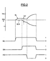
- the only precharge circuit 2 at the bottom of the column, i.e. opposite the memory cell with respect to means for amplifying and rendering the decoupling transistors NMOS T6 and T9 controllable on their grid by a second signal control (not shown in Figure 1 for the purpose of simplification) instead of connecting their grid constantly to the voltage of VDD polarization.
- a second signal control not shown in Figure 1 for the purpose of simplification
Landscapes
- Engineering & Computer Science (AREA)
- Microelectronics & Electronic Packaging (AREA)
- Computer Hardware Design (AREA)
- Dram (AREA)
Claims (9)
- Vorrichtung zum Lesen und Überschreiben einer Speicherzelle eines in Zeilen und Spalten organisierten dynamischen Speichers, der für jede Spalte eine Voraufladeeinrichtung (2) und eine Verstärkungseinrichtung aufweist, die zwei Inverter (T4, T5, T7, T8) aufweist, die jeweils mit zwei komplementären und von zwei aufeinanderfolgenden Lese- (SN) und Überschreib- (RS) Signalen gesteuerten Transistoren gebildet sind, wobei die Verstärkungseinrichtung eine Entkopplungsstruktur aufweist, die mit zwei Paaren von parallel geschalteten komplementären Entkopplungstransistoren (T6, T10, T9, T11) gebildet ist, wobei eines der Paare zwischen den zwei Transistoren des einen Inverters angeschlossen ist und das andere Paar zwischen den zwei Transistoren des anderen Inverters angeschlossen ist, dadurch gekennzeichnet, daß die Entkopplungsstruktur auf einen Befehl hin mindestens einen ersten Zustand, in welchem alle Entkopplungstransistoren leitend sind, und einen zweiten Zustand einnehmen kann, in welchem die zwei Entkopplungstransistoren (T9, T6), die einen Kanal des gleichen Leitungstyps haben, leitend sind, während die zwei anderen Entkopplungstransistoren (T10, T11) gesperrt sind.
- Vorrichtung nach Anspruch 1, dadurch gekennzeichnet, daß die Voraufladeeinrichtung nur eine einzige Voraufladeschaltung (2) aufweist, die parallel zur Verstärkungseinrichtung und, bezogen auf die Verstärkungseinrichtung, auf der gleichen Seite wie die Speicherzelle (CM) oder auf der zur Speicherzelle entgegengesetzten Seite angeordnet ist.
- Vorrichtung nach einem der vorstehenden Ansprüche, dadurch gekennzeichnet, daß die Gatter zweier Entkopplungstransistoren (T6, T9), die einen gleichen Kanaltyp haben, mit einer vorgegebenen Vorspannung (VDD) verbunden sind, so daß diese zwei Entkopplungstransistoren immer leitend sind, wobei die Gatter der zwei anderen Entkopplungstransistoren (T10, T11) von einem gleichen Steuersignal (Cmd) in zwei logische Zustände gesteuert werden, so daß diese zwei anderen Entkopplungstransistoren leitend oder sperrend gemacht sind.
- Vorrichtung nach Anspruch 2, dadurch gekennzeichnet, daß die Voraufladeschaltung (2) parallel zur Verstärkungseinrichtung und, bezogen auf die Verstärkungseinrichtung, auf der zur Speicherzelle entgegengesetzten Seite angeordnet ist, und dadurch, daß die Entkopplungsstruktur einen dritten Zustand einnehmen kann, in welchem alle Entkopplungstransistoren gesperrt sind.
- Vorrichtung nach Anspruch 4, dadurch gekennzeichnet, daß die Gatter zweier Entkopplungstransistoren (T6, T9), die einen gleichen Kanaltyp haben, von einem gleichen ersten Steuersignal in zwei logische Zustände gesteuert werden, so daß diese zwei Entkopplungstransistoren leitend oder sperrend gemacht sind, und die Gatter der zwei anderen Entkopplungstransistoren (T10, T11) von einem gleichen zweiten Steuersignal in zwei logische Zustände gesteuert werden, so daß diese zwei anderen Entkopplungstransistoren leitend oder sperrend gemacht sind.
- Verfahren zur Steuerung einer Lese/Überschreib-Vorrichtung nach Anspruch 1, in welchem im Verlaufe eines Zyklus des Schreibens in die Speicherzelle die Entkopplungsstruktur in ihren ersten Zustand gebracht wird und nach einer Voraufladephase im Verlaufe eines Zyklus des Lesens/Überschreibens die Entkopplungsstruktur in ihren zweiten Zustand gebracht wird.
- Verfahren nach Anspruch 6 für eine Vorrichtung, deren Voraufladeeinrichtung nur eine einzige Voraufladeschaltung (2) aufweist, die parallel zur Verstärkungseinrichtung und, bezogen auf die Verstärkungseinrichtung, auf der gleichen Seite wie die Speicherzelle oder auf der zur Speicherzelle entgegengesetzten Seite angeordnet ist, dadurch gekennzeichnet, daß im Verlaufe mindestens eines Teils der Voraufladephase die Entkopplungsstruktur in ihren ersten Zustand gebracht wird.
- Verfahren nach Anspruch 7, dadurch gekennzeichnet, daß während der gesamten Voraufladephase die Entkopplungsstruktur in ihren ersten Zustand gebracht ist.
- Verfahren nach Anspruch 7 für eine Vorrichtung, deren einzige Voraufladeschaltung (2) parallel zur Verstärkungseinrichtung und, bezogen auf die Verstärkungseinrichtung, auf der zur Speicherzelle entgegengesetzten Seite angeschlossen ist, und deren Entkopplungsstruktur einen dritten Zustand einnehmen kann, in welchem alle Entkopplungstransistoren gesperrt sind, dadurch gekennzeichnet, daß während der Voraufladephase die Entkopplungsstruktur in ihren ersten Zustand gebracht ist, und dann unmittelbar vor Deaktivieren der Voraufladeeinrichtung (2) die Entkopplungsstruktur in ihren dritten Zustand gebracht wird.
Applications Claiming Priority (2)
| Application Number | Priority Date | Filing Date | Title |
|---|---|---|---|
| FR9711807A FR2768847B1 (fr) | 1997-09-23 | 1997-09-23 | Dispositif et procede de lecture/re-ecriture d'une cellule-memoire vive dynamique |
| FR9711807 | 1997-09-23 |
Publications (2)
| Publication Number | Publication Date |
|---|---|
| EP0903746A1 EP0903746A1 (de) | 1999-03-24 |
| EP0903746B1 true EP0903746B1 (de) | 2003-12-17 |
Family
ID=9511359
Family Applications (1)
| Application Number | Title | Priority Date | Filing Date |
|---|---|---|---|
| EP98402186A Expired - Lifetime EP0903746B1 (de) | 1997-09-23 | 1998-09-04 | Verfahren und Vorrichtung zum Lesen und Überschreiben einer dynamischen Speicherzelle |
Country Status (4)
| Country | Link |
|---|---|
| US (1) | US5936904A (de) |
| EP (1) | EP0903746B1 (de) |
| DE (1) | DE69820555D1 (de) |
| FR (1) | FR2768847B1 (de) |
Families Citing this family (3)
| Publication number | Priority date | Publication date | Assignee | Title |
|---|---|---|---|---|
| FR2774209B1 (fr) * | 1998-01-23 | 2001-09-14 | St Microelectronics Sa | Procede de controle du circuit de lecture d'un plan memoire et dispositif de memoire correspondant |
| FR2775382B1 (fr) * | 1998-02-25 | 2001-10-05 | St Microelectronics Sa | Procede de controle du rafraichissement d'un plan memoire d'un dispositif de memoire vive dynamique, et dispositif de memoire vive correspondant |
| US9679619B2 (en) * | 2013-03-15 | 2017-06-13 | Taiwan Semiconductor Manufacturing Company, Ltd. | Sense amplifier with current regulating circuit |
Family Cites Families (6)
| Publication number | Priority date | Publication date | Assignee | Title |
|---|---|---|---|---|
| US3959781A (en) * | 1974-11-04 | 1976-05-25 | Intel Corporation | Semiconductor random access memory |
| US4816706A (en) * | 1987-09-10 | 1989-03-28 | International Business Machines Corporation | Sense amplifier with improved bitline precharging for dynamic random access memory |
| JPH0696582A (ja) * | 1990-09-17 | 1994-04-08 | Texas Instr Inc <Ti> | メモリアレイアーキテクチャ |
| US5241503A (en) * | 1991-02-25 | 1993-08-31 | Motorola, Inc. | Dynamic random access memory with improved page-mode performance and method therefor having isolator between memory cells and sense amplifiers |
| US5339274A (en) * | 1992-10-30 | 1994-08-16 | International Business Machines Corporation | Variable bitline precharge voltage sensing technique for DRAM structures |
| KR0142952B1 (ko) * | 1995-03-31 | 1998-08-17 | 김광호 | 반도체 메모리장치의 감지증폭기 회로 |
-
1997
- 1997-09-23 FR FR9711807A patent/FR2768847B1/fr not_active Expired - Fee Related
-
1998
- 1998-09-04 EP EP98402186A patent/EP0903746B1/de not_active Expired - Lifetime
- 1998-09-04 DE DE69820555T patent/DE69820555D1/de not_active Expired - Lifetime
- 1998-09-09 US US09/150,255 patent/US5936904A/en not_active Expired - Lifetime
Also Published As
| Publication number | Publication date |
|---|---|
| FR2768847B1 (fr) | 2001-05-18 |
| DE69820555D1 (de) | 2004-01-29 |
| FR2768847A1 (fr) | 1999-03-26 |
| EP0903746A1 (de) | 1999-03-24 |
| US5936904A (en) | 1999-08-10 |
Similar Documents
| Publication | Publication Date | Title |
|---|---|---|
| FR2774209A1 (fr) | Procede de controle du circuit de lecture d'un plan memoire et dispositif de memoire correspondant | |
| FR2799874A1 (fr) | Dispositif de memoire a semiconducteur | |
| JP4191278B2 (ja) | 高速書込みリカバリを備えたメモリ装置および関連する書込みリカバリ方法 | |
| FR2974666A1 (fr) | Amplificateur de detection differentiel sans transistor de precharge dedie | |
| FR2898432A1 (fr) | Cellules memoire en technologie cmos double-grille dotee de transistors a deux grilles independantes | |
| EP0279712B1 (de) | Speicher-Leseschaltung | |
| FR2957449A1 (fr) | Micro-amplificateur de lecture pour memoire | |
| FR2974667A1 (fr) | Amplificateur de detection differentiel sans transistor de commutation | |
| EP1434237A1 (de) | Nichtflüchtige SRAM Speicherzelle | |
| US6400629B1 (en) | System and method for early write to memory by holding bitline at fixed potential | |
| US20060268615A1 (en) | Nonvolatile semiconductor static random access memory device | |
| EP0516516A1 (de) | Speicher mit kapazitiver EEPROM-Speicherzelle und Verfahren zum Lesen dieser Speicherzelle | |
| FR2775382A1 (fr) | Procede de controle du rafraichissement d'un plan memoire d'un dispositif de memoire vive dynamique, et dispositif de memoire vive correspondant | |
| EP0903746B1 (de) | Verfahren und Vorrichtung zum Lesen und Überschreiben einer dynamischen Speicherzelle | |
| FR2702873A1 (fr) | Cellule mémoire insensible aux collisions d'ions lourds. | |
| EP0897182B1 (de) | Strahlungsunempfindliche statische Speicherzelle | |
| FR2811132A1 (fr) | Circuit de memoire dynamique comportant des cellules de secours | |
| EP1164592A1 (de) | Dynamische Speicheranordnung mit wahlfreiem Zugriff sowie entsprechendes Leseverfahren | |
| EP1168359B1 (de) | Vefahren zur Steurung eines Lesezugriffs auf einen dynamischen Speicher und Speicher dazu | |
| FR2824176A1 (fr) | Procede et dispositif de lecture de cellules de memoire dynamique | |
| FR2823362A1 (fr) | Dispositif de lecture de cellules memoire | |
| EP0910094B1 (de) | Dynamische Speicheranordnung mit verkürzter Auffrischungszeit und entsprechende Auffrischungsverfahren | |
| FR2600808A1 (fr) | Plan memoire a lecture rapide | |
| EP1103979A1 (de) | Dynamische Speicheranordnung mit wahlfreiem Zugriff (DRAM) sowie entsprechendes Leseverfahren | |
| FR2773635A1 (fr) | Dispositif et procede de lecture re-ecriture d'une cellule-memoire vive dynamique |
Legal Events
| Date | Code | Title | Description |
|---|---|---|---|
| PUAI | Public reference made under article 153(3) epc to a published international application that has entered the european phase |
Free format text: ORIGINAL CODE: 0009012 |
|
| AK | Designated contracting states |
Kind code of ref document: A1 Designated state(s): DE FR GB IT |
|
| AX | Request for extension of the european patent |
Free format text: AL;LT;LV;MK;RO;SI |
|
| 17P | Request for examination filed |
Effective date: 19990623 |
|
| AKX | Designation fees paid |
Free format text: DE FR GB IT |
|
| RAP1 | Party data changed (applicant data changed or rights of an application transferred) |
Owner name: STMICROELECTRONICS S.A. |
|
| GRAH | Despatch of communication of intention to grant a patent |
Free format text: ORIGINAL CODE: EPIDOS IGRA |
|
| GRAH | Despatch of communication of intention to grant a patent |
Free format text: ORIGINAL CODE: EPIDOS IGRA |
|
| GRAA | (expected) grant |
Free format text: ORIGINAL CODE: 0009210 |
|
| AK | Designated contracting states |
Kind code of ref document: B1 Designated state(s): DE FR GB IT |
|
| PG25 | Lapsed in a contracting state [announced via postgrant information from national office to epo] |
Ref country code: IT Free format text: LAPSE BECAUSE OF FAILURE TO SUBMIT A TRANSLATION OF THE DESCRIPTION OR TO PAY THE FEE WITHIN THE PRESCRIBED TIME-LIMIT;WARNING: LAPSES OF ITALIAN PATENTS WITH EFFECTIVE DATE BEFORE 2007 MAY HAVE OCCURRED AT ANY TIME BEFORE 2007. THE CORRECT EFFECTIVE DATE MAY BE DIFFERENT FROM THE ONE RECORDED. Effective date: 20031217 |
|
| REG | Reference to a national code |
Ref country code: GB Ref legal event code: FG4D Free format text: NOT ENGLISH |
|
| GBT | Gb: translation of ep patent filed (gb section 77(6)(a)/1977) |
Effective date: 20031217 |
|
| REF | Corresponds to: |
Ref document number: 69820555 Country of ref document: DE Date of ref document: 20040129 Kind code of ref document: P |
|
| PG25 | Lapsed in a contracting state [announced via postgrant information from national office to epo] |
Ref country code: DE Free format text: LAPSE BECAUSE OF FAILURE TO SUBMIT A TRANSLATION OF THE DESCRIPTION OR TO PAY THE FEE WITHIN THE PRESCRIBED TIME-LIMIT Effective date: 20040318 |
|
| PLBE | No opposition filed within time limit |
Free format text: ORIGINAL CODE: 0009261 |
|
| STAA | Information on the status of an ep patent application or granted ep patent |
Free format text: STATUS: NO OPPOSITION FILED WITHIN TIME LIMIT |
|
| 26N | No opposition filed |
Effective date: 20040920 |
|
| PGFP | Annual fee paid to national office [announced via postgrant information from national office to epo] |
Ref country code: GB Payment date: 20060831 Year of fee payment: 9 |
|
| PGFP | Annual fee paid to national office [announced via postgrant information from national office to epo] |
Ref country code: FR Payment date: 20070926 Year of fee payment: 10 |
|
| GBPC | Gb: european patent ceased through non-payment of renewal fee |
Effective date: 20070904 |
|
| PG25 | Lapsed in a contracting state [announced via postgrant information from national office to epo] |
Ref country code: GB Free format text: LAPSE BECAUSE OF NON-PAYMENT OF DUE FEES Effective date: 20070904 |
|
| REG | Reference to a national code |
Ref country code: FR Ref legal event code: ST Effective date: 20090529 |
|
| PG25 | Lapsed in a contracting state [announced via postgrant information from national office to epo] |
Ref country code: FR Free format text: LAPSE BECAUSE OF NON-PAYMENT OF DUE FEES Effective date: 20080930 |