EP1164823A2 - Printed circuit board and method of manufacturing the same - Google Patents

Printed circuit board and method of manufacturing the same Download PDF

Info

Publication number
EP1164823A2
EP1164823A2 EP01113580A EP01113580A EP1164823A2 EP 1164823 A2 EP1164823 A2 EP 1164823A2 EP 01113580 A EP01113580 A EP 01113580A EP 01113580 A EP01113580 A EP 01113580A EP 1164823 A2 EP1164823 A2 EP 1164823A2
Authority
EP
European Patent Office
Prior art keywords
circuit board
printed circuit
dielectric substrate
conductor
epoxy resin
Prior art date
Legal status (The legal status is an assumption and is not a legal conclusion. Google has not performed a legal analysis and makes no representation as to the accuracy of the status listed.)
Withdrawn
Application number
EP01113580A
Other languages
German (de)
French (fr)
Other versions
EP1164823A3 (en
Inventor
Daizo Andoh
Fumio Echigo
Tadashi Nakamura
Yasuhiro Nakatani
Yoji Ueda
Tousaku Nishiyama
Shozo Ochi
Current Assignee (The listed assignees may be inaccurate. Google has not performed a legal analysis and makes no representation or warranty as to the accuracy of the list.)
Panasonic Holdings Corp
Original Assignee
Matsushita Electric Industrial Co Ltd
Priority date (The priority date is an assumption and is not a legal conclusion. Google has not performed a legal analysis and makes no representation as to the accuracy of the date listed.)
Filing date
Publication date
Application filed by Matsushita Electric Industrial Co Ltd filed Critical Matsushita Electric Industrial Co Ltd
Publication of EP1164823A2 publication Critical patent/EP1164823A2/en
Publication of EP1164823A3 publication Critical patent/EP1164823A3/en
Withdrawn legal-status Critical Current

Links

Images

Classifications

    • HELECTRICITY
    • H05ELECTRIC TECHNIQUES NOT OTHERWISE PROVIDED FOR
    • H05KPRINTED CIRCUITS; CASINGS OR CONSTRUCTIONAL DETAILS OF ELECTRIC APPARATUS; MANUFACTURE OF ASSEMBLAGES OF ELECTRICAL COMPONENTS
    • H05K3/00Apparatus or processes for manufacturing printed circuits
    • H05K3/40Forming printed elements for providing electric connections to or between printed circuits
    • H05K3/4038Through-connections; Vertical interconnect access [VIA] connections
    • H05K3/4053Through-connections; Vertical interconnect access [VIA] connections by thick-film techniques
    • H05K3/4069Through-connections; Vertical interconnect access [VIA] connections by thick-film techniques for via connections in organic insulating substrates
    • HELECTRICITY
    • H05ELECTRIC TECHNIQUES NOT OTHERWISE PROVIDED FOR
    • H05KPRINTED CIRCUITS; CASINGS OR CONSTRUCTIONAL DETAILS OF ELECTRIC APPARATUS; MANUFACTURE OF ASSEMBLAGES OF ELECTRICAL COMPONENTS
    • H05K1/00Printed circuits
    • H05K1/02Details
    • H05K1/03Use of materials for the substrate
    • H05K1/0313Organic insulating material
    • H05K1/0353Organic insulating material consisting of two or more materials, e.g. two or more polymers, polymer + filler, + reinforcement
    • H05K1/0366Organic insulating material consisting of two or more materials, e.g. two or more polymers, polymer + filler, + reinforcement reinforced, e.g. by fibres, fabrics
    • HELECTRICITY
    • H05ELECTRIC TECHNIQUES NOT OTHERWISE PROVIDED FOR
    • H05KPRINTED CIRCUITS; CASINGS OR CONSTRUCTIONAL DETAILS OF ELECTRIC APPARATUS; MANUFACTURE OF ASSEMBLAGES OF ELECTRICAL COMPONENTS
    • H05K1/00Printed circuits
    • H05K1/02Details
    • H05K1/03Use of materials for the substrate
    • H05K1/0313Organic insulating material
    • H05K1/0353Organic insulating material consisting of two or more materials, e.g. two or more polymers, polymer + filler, + reinforcement
    • H05K1/0373Organic insulating material consisting of two or more materials, e.g. two or more polymers, polymer + filler, + reinforcement containing additives, e.g. fillers
    • HELECTRICITY
    • H05ELECTRIC TECHNIQUES NOT OTHERWISE PROVIDED FOR
    • H05KPRINTED CIRCUITS; CASINGS OR CONSTRUCTIONAL DETAILS OF ELECTRIC APPARATUS; MANUFACTURE OF ASSEMBLAGES OF ELECTRICAL COMPONENTS
    • H05K2201/00Indexing scheme relating to printed circuits covered by H05K1/00
    • H05K2201/02Fillers; Particles; Fibers; Reinforcement materials
    • H05K2201/0203Fillers and particles
    • H05K2201/0263Details about a collection of particles
    • H05K2201/0266Size distribution
    • HELECTRICITY
    • H05ELECTRIC TECHNIQUES NOT OTHERWISE PROVIDED FOR
    • H05KPRINTED CIRCUITS; CASINGS OR CONSTRUCTIONAL DETAILS OF ELECTRIC APPARATUS; MANUFACTURE OF ASSEMBLAGES OF ELECTRICAL COMPONENTS
    • H05K2201/00Indexing scheme relating to printed circuits covered by H05K1/00
    • H05K2201/03Conductive materials
    • H05K2201/0332Structure of the conductor
    • H05K2201/0335Layered conductors or foils
    • H05K2201/0355Metal foils
    • HELECTRICITY
    • H05ELECTRIC TECHNIQUES NOT OTHERWISE PROVIDED FOR
    • H05KPRINTED CIRCUITS; CASINGS OR CONSTRUCTIONAL DETAILS OF ELECTRIC APPARATUS; MANUFACTURE OF ASSEMBLAGES OF ELECTRICAL COMPONENTS
    • H05K2201/00Indexing scheme relating to printed circuits covered by H05K1/00
    • H05K2201/10Details of components or other objects attached to or integrated in a printed circuit board
    • H05K2201/10227Other objects, e.g. metallic pieces
    • H05K2201/10378Interposers
    • HELECTRICITY
    • H05ELECTRIC TECHNIQUES NOT OTHERWISE PROVIDED FOR
    • H05KPRINTED CIRCUITS; CASINGS OR CONSTRUCTIONAL DETAILS OF ELECTRIC APPARATUS; MANUFACTURE OF ASSEMBLAGES OF ELECTRICAL COMPONENTS
    • H05K2203/00Indexing scheme relating to apparatus or processes for manufacturing printed circuits covered by H05K3/00
    • H05K2203/01Tools for processing; Objects used during processing
    • H05K2203/0191Using tape or non-metallic foil in a process, e.g. during filling of a hole with conductive paste
    • HELECTRICITY
    • H05ELECTRIC TECHNIQUES NOT OTHERWISE PROVIDED FOR
    • H05KPRINTED CIRCUITS; CASINGS OR CONSTRUCTIONAL DETAILS OF ELECTRIC APPARATUS; MANUFACTURE OF ASSEMBLAGES OF ELECTRICAL COMPONENTS
    • H05K2203/00Indexing scheme relating to apparatus or processes for manufacturing printed circuits covered by H05K3/00
    • H05K2203/14Related to the order of processing steps
    • H05K2203/1461Applying or finishing the circuit pattern after another process, e.g. after filling of vias with conductive paste, after making printed resistors
    • HELECTRICITY
    • H05ELECTRIC TECHNIQUES NOT OTHERWISE PROVIDED FOR
    • H05KPRINTED CIRCUITS; CASINGS OR CONSTRUCTIONAL DETAILS OF ELECTRIC APPARATUS; MANUFACTURE OF ASSEMBLAGES OF ELECTRICAL COMPONENTS
    • H05K3/00Apparatus or processes for manufacturing printed circuits
    • H05K3/46Manufacturing multilayer circuits
    • H05K3/4611Manufacturing multilayer circuits by laminating two or more circuit boards
    • H05K3/4614Manufacturing multilayer circuits by laminating two or more circuit boards the electrical connections between the circuit boards being made during lamination
    • HELECTRICITY
    • H05ELECTRIC TECHNIQUES NOT OTHERWISE PROVIDED FOR
    • H05KPRINTED CIRCUITS; CASINGS OR CONSTRUCTIONAL DETAILS OF ELECTRIC APPARATUS; MANUFACTURE OF ASSEMBLAGES OF ELECTRICAL COMPONENTS
    • H05K3/00Apparatus or processes for manufacturing printed circuits
    • H05K3/46Manufacturing multilayer circuits
    • H05K3/4611Manufacturing multilayer circuits by laminating two or more circuit boards
    • H05K3/4614Manufacturing multilayer circuits by laminating two or more circuit boards the electrical connections between the circuit boards being made during lamination
    • H05K3/462Manufacturing multilayer circuits by laminating two or more circuit boards the electrical connections between the circuit boards being made during lamination characterized by laminating only or mainly similar double-sided circuit boards
    • HELECTRICITY
    • H05ELECTRIC TECHNIQUES NOT OTHERWISE PROVIDED FOR
    • H05KPRINTED CIRCUITS; CASINGS OR CONSTRUCTIONAL DETAILS OF ELECTRIC APPARATUS; MANUFACTURE OF ASSEMBLAGES OF ELECTRICAL COMPONENTS
    • H05K3/00Apparatus or processes for manufacturing printed circuits
    • H05K3/46Manufacturing multilayer circuits
    • H05K3/4644Manufacturing multilayer circuits by building the multilayer layer by layer, i.e. build-up multilayer circuits
    • H05K3/4652Adding a circuit layer by laminating a metal foil or a preformed metal foil pattern
    • YGENERAL TAGGING OF NEW TECHNOLOGICAL DEVELOPMENTS; GENERAL TAGGING OF CROSS-SECTIONAL TECHNOLOGIES SPANNING OVER SEVERAL SECTIONS OF THE IPC; TECHNICAL SUBJECTS COVERED BY FORMER USPC CROSS-REFERENCE ART COLLECTIONS [XRACs] AND DIGESTS
    • Y10TECHNICAL SUBJECTS COVERED BY FORMER USPC
    • Y10TTECHNICAL SUBJECTS COVERED BY FORMER US CLASSIFICATION
    • Y10T29/00Metal working
    • Y10T29/49Method of mechanical manufacture
    • Y10T29/49002Electrical device making
    • Y10T29/49117Conductor or circuit manufacturing
    • Y10T29/49124On flat or curved insulated base, e.g., printed circuit, etc.
    • Y10T29/49126Assembling bases
    • YGENERAL TAGGING OF NEW TECHNOLOGICAL DEVELOPMENTS; GENERAL TAGGING OF CROSS-SECTIONAL TECHNOLOGIES SPANNING OVER SEVERAL SECTIONS OF THE IPC; TECHNICAL SUBJECTS COVERED BY FORMER USPC CROSS-REFERENCE ART COLLECTIONS [XRACs] AND DIGESTS
    • Y10TECHNICAL SUBJECTS COVERED BY FORMER USPC
    • Y10TTECHNICAL SUBJECTS COVERED BY FORMER US CLASSIFICATION
    • Y10T29/00Metal working
    • Y10T29/49Method of mechanical manufacture
    • Y10T29/49002Electrical device making
    • Y10T29/49117Conductor or circuit manufacturing
    • Y10T29/49124On flat or curved insulated base, e.g., printed circuit, etc.
    • Y10T29/49155Manufacturing circuit on or in base
    • YGENERAL TAGGING OF NEW TECHNOLOGICAL DEVELOPMENTS; GENERAL TAGGING OF CROSS-SECTIONAL TECHNOLOGIES SPANNING OVER SEVERAL SECTIONS OF THE IPC; TECHNICAL SUBJECTS COVERED BY FORMER USPC CROSS-REFERENCE ART COLLECTIONS [XRACs] AND DIGESTS
    • Y10TECHNICAL SUBJECTS COVERED BY FORMER USPC
    • Y10TTECHNICAL SUBJECTS COVERED BY FORMER US CLASSIFICATION
    • Y10T29/00Metal working
    • Y10T29/49Method of mechanical manufacture
    • Y10T29/49002Electrical device making
    • Y10T29/49117Conductor or circuit manufacturing
    • Y10T29/49124On flat or curved insulated base, e.g., printed circuit, etc.
    • Y10T29/49155Manufacturing circuit on or in base
    • Y10T29/49165Manufacturing circuit on or in base by forming conductive walled aperture in base
    • YGENERAL TAGGING OF NEW TECHNOLOGICAL DEVELOPMENTS; GENERAL TAGGING OF CROSS-SECTIONAL TECHNOLOGIES SPANNING OVER SEVERAL SECTIONS OF THE IPC; TECHNICAL SUBJECTS COVERED BY FORMER USPC CROSS-REFERENCE ART COLLECTIONS [XRACs] AND DIGESTS
    • Y10TECHNICAL SUBJECTS COVERED BY FORMER USPC
    • Y10TTECHNICAL SUBJECTS COVERED BY FORMER US CLASSIFICATION
    • Y10T428/00Stock material or miscellaneous articles
    • Y10T428/24Structurally defined web or sheet [e.g., overall dimension, etc.]
    • Y10T428/24802Discontinuous or differential coating, impregnation or bond [e.g., artwork, printing, retouched photograph, etc.]
    • Y10T428/24917Discontinuous or differential coating, impregnation or bond [e.g., artwork, printing, retouched photograph, etc.] including metal layer

Definitions

  • the entire dielectric substrate When the dielectric substrate after being applied with heat and pressure is substantially uniform in thickness in the center and in the periphery, the entire dielectric substrate will be applied with uniform compression at a time of applying heat and pressure, and thus, variation in the connection resistance can be reduced.
  • Example 5 is a graph to show the dependence of an initial resistance value on the thickness of the resin layer of the material included in a printed circuit board. Since the initial resistance value is lowered as the resin layer of the material is thinned, the material in Example 1 was determined to be 130 ⁇ m in thickness.
  • the mold-releasing films used here were polyethylene terephthalate (PET) 19 ⁇ m in thickness.
  • PET polyethylene terephthalate
  • the glass cloth used for the dielectric substrate can be replaced by a glass nonwoven fabric on which resin layers are formed.
  • a core substrate 201 was prepared in the same process as indicated in FIG. 1F of Example 1.

Landscapes

  • Engineering & Computer Science (AREA)
  • Microelectronics & Electronic Packaging (AREA)
  • Manufacturing & Machinery (AREA)
  • Production Of Multi-Layered Print Wiring Board (AREA)
  • Printing Elements For Providing Electric Connections Between Printed Circuits (AREA)

Abstract
The present invention provides a printed circuit board, which includes a dielectric substrate (201) having via holes formed in the thickness direction, and a conductor (205) including a conductive filler is filled in the via holes. The dielectric substrate (201) has patterned wiring layers (204, 206, 208) on both surfaces, and the wiring layers (204, 206, 208) are connected electrically with each other by the conductor (205). The dielectric substrate (201) is made of a glass cloth or a glass nonwoven fabric impregnated with a thermosetting epoxy resin mixed with fine particles, and the conductive filler in the conductor (205) has an average particle diameter larger than that of the fine particles. Accordingly, the printed circuit board has an improved moisture resistance as a whole and also excellent connection reliability and repair resistance. In addition, the dielectric substrate (201) of the printed circuit board has an improved mechanical strength such as flexural rigidity. The present invention also provides a method of manufacturing such a printed circuit board.
Figure 00000001
Figure 00000002

Description

This invention relates to a printed circuit board that is suitable for high density packaging of various high-performance electronic apparatuses. The printed circuit board has excellent flexural rigidity or moisture absorption and repair resistance. This invention relates to also a method of manufacturing such a printed circuit board.
Recently, various electronic elements composing electronic apparatuses have become smaller and thinner since electronic apparatuses have become small, thin, light-weight and better in the performance. Printed circuit boards for packaging these electronic elements also have been developed to provide a high density package.
With a rapid progress in packaging techniques, it is desired to supply circuit boards with a multilayer wiring structure at a low cost. Such a circuit board can be manufactured by mounting bare chips of a semiconductor device such as LSI directly at a high density, and it can correspond to a high-speed signal processing circuit. Such a multilayer circuit board is required to have high reliability in electric connection between wiring patterns of plural layers formed with a minute wiring pitch and also excellent high frequency property, and is required to have high reliability in a connection with a semiconductor bare chip.
For satisfying this requirement, a resin multilayer circuit board having an any-layer IVH structure is proposed in JP-A-6-268345. In this reference, a copper-plated conductor on a through-hole inner wall, which mainly has been used for interlayer connection in a conventional multilayer circuit board, is replaced by filling of a conductor in a interstitial via hole (IVH) and at the same time, the IVH can be formed immediate below an element land or between arbitrary layers, so that substrate size can be decreased and a high density packaging can be provided. FIGs. 12A-12G show a method of manufacturing such a printed circuit board. First, as shown in FIG. 12A, mold-releasing films 401 made of polyester or the like are laminated on both surfaces of a porous substrate 402 such as an aramid epoxy pre-preg prepared by impregnating an aramid nonwoven fabric with a thermosetting epoxy resin. Next, as shown in FIG. 12B, via holes 403 are formed at predetermined positions of the porous substrate 402 by laser beam machining. Subsequently as shown in FIG. 12C, a conductive paste 404 is filled in the via holes 403. In this step, the porous substrate 402 with the via holes 403 is placed on a table of a screen printer, and the conductive paste 404 is directly printed on the mold-releasing film 401. The mold-releasing films 401 on the printing surface function as printing masks and prevent contamination of the surface of the porous substrate 402. Next, the mold-releasing films 401 are peeled off from the surfaces of the porous substrate 402, and then, metal foils 405 e.g., copper foils, are adhered to the surfaces of the porous substrate 402. By applying heat and pressure in this condition, the porous substrate 402 is compressed and thinned as shown in FIG. 12D. At that time, the conductive paste 404 in the via holes 403 also is compressed and binder ingredients contained in the conductive paste is extruded to strengthen bonding among the conductive ingredients and also between the conductive ingredients and metal foils 405. As a result, the conductive substance in the conductive paste 404 is condensed and the layers are connected electrically with each other. Subsequently, the conductive paste 404 and the thermosetting resin composing the porous substrate 402 are cured. The metal foils 405 are etched selectively to have a predetermined pattern so that a double-sided circuit board as shown in FIG. 12E is provided. Further, as shown in FIG. 12F, porous substrates 406 and metal foils 407 are stuck to the surfaces of the double-sided circuit board by using a conductive paste 408. After applying heat and pressure, as shown in FIG. 12G, the metal foils 407 are etched to have a predetermined pattern, so that a multilayer circuit board is obtained.
Resin multilayer substrates formed by using such substrates for forming circuits have been used for many electronic apparatuses because they have low coefficient of expansion, low dielectric constant, and light-weight.
However, a resin multilayer circuit board having the above-mentioned any-layer IVH structure has a core of an aramid nonwoven fabric, and a dielectric substrate is composed of a homogeneous mixture of an epoxy resin and aramid nonwoven fabric fibers. Such a dielectric substrate having a core of aramid nonwoven fabric has a coefficient of thermal expansion (CTE) of about 100 ppm/°C in the thickness direction, which is different considerably from CTE (about 17 ppm/°C) of an interstitial via conductor forming the any-layer IVH structure.
Since the properties of the electronic apparatus may deteriorate to some degree under a severe use condition with abrupt change in temperature, printed circuit boards with higher reliability have been desired.
In order to solve the above-mentioned problems, a first purpose of the present invention is to provide a printed circuit board and a method of manufacturing the printed circuit board. The printed circuit board has an improved moisture resistance as a whole, so that the connection reliability and repair resistance are improved, and the printed circuit board comprises a dielectric substrate with improved mechanical strength e.g., flexural rigidity.
In addition to the first purpose, a second purpose is to provide a printed circuit board with improved adherence between a wiring pattern and a dielectric substrate and connection reliability between the wiring pattern and the interstitial via conductor, which is achieved by reducing the coefficient of thermal expansion (CTE) of the entire dielectric substrate.
For achieving the purposes, a first printed circuit board according to the present invention comprises a dielectric substrate having via holes formed in the thickness direction in which a conductor containing a conductive filler is filled, and wiring layers are formed on both surfaces of the dielectric substrate so as to have a predetermined pattern and connected electrically with each other by the conductor. The printed circuit board is characterized in that the dielectric substrate is made of a glass cloth or a glass nonwoven fabric impregnated with a thermosetting epoxy resin mixed with fine particles, and the conductive filler contained in the conductor has an average particle diameter larger than that of the fine particles.
A second printed circuit board according to the present invention comprises an internal circuit board and external circuit boards provided on both surfaces of the internal circuit board. The internal circuit board comprises at least two layers of a wiring pattern connected by first interstitial via conductors. The external circuit boards comprise a dielectric material of a glass epoxy resin, second interstitial via conductors compressed into the dielectric substrate to have conductivity and also second wiring patterns arranged on the outermost surfaces of the dielectric substrate. The second printed circuit boards are characterized in that the first wiring pattern on the surfaces of the internal circuit board and the second wiring patterns of the external circuit boards are connected electrically with each other.
A first manufacturing method according to the present invention comprises steps of:
  • preparing a dielectric substrate of a pre-preg formed by impregnating a glass cloth or a glass nonwoven fabric with a thermosetting epoxy resin mixed with fine particles,
  • coating both surfaces of the dielectric substrate with mold-releasing films and subsequently forming a via hole,
  • filling in the via hole with a conductor containing a conductive filler having an average particle diameter larger than the average diameter of the fine particles,
  • peeling the mold-releasing films and layering metal foils on the surfaces of the dielectric substrate,
  • compressing the dielectric substrate having the metal foils by applying heat and pressure in order to adhere the dielectric substrate and the metal foils and to connect electrically the metal foils with each other, and
  • forming the metal foils to have a predetermined pattern.
  • A second manufacturing method according to the present invention comprises steps of:
  • preparing an internal circuit board having at least two layers of first wiring patterns protruding from surfaces of the internal circuit board and being connected with each other by first interstitial via conductors,
  • preparing glass epoxy resin dielectric substrates in a pre-preg stage by forming via holes at arbitrary positions and filling a conductive paste to make a second interstitial via conductor,
  • arranging the glass epoxy resin dielectric substrates on both surfaces of the internal circuit board,
  • arranging copper foils on outer surfaces of the respective glass epoxy resin dielectric substrates,
  • applying heat and pressure from outside of the two copper foils the internal circuit board and the glass epoxy resin dielectric substrates in a pre-preg stage so as to force the protruding wiring patterns of the internal circuit board into the glass epoxy resin dielectric substrate in a pre-preg stage and at the same time to compress the conductive paste provided to the glass epoxy resin dielectric substrates for connecting electrically the outermost copper foils and the first wiring patterns in the internal circuit board, and subsequently
  • etching the copper foils selectively to form second wiring patterns and so as to configure external circuit boards.
  • FIGs. 1A-1F are cross-sectional views to show steps of manufacturing a printed circuit board in Example 1 of the present invention.
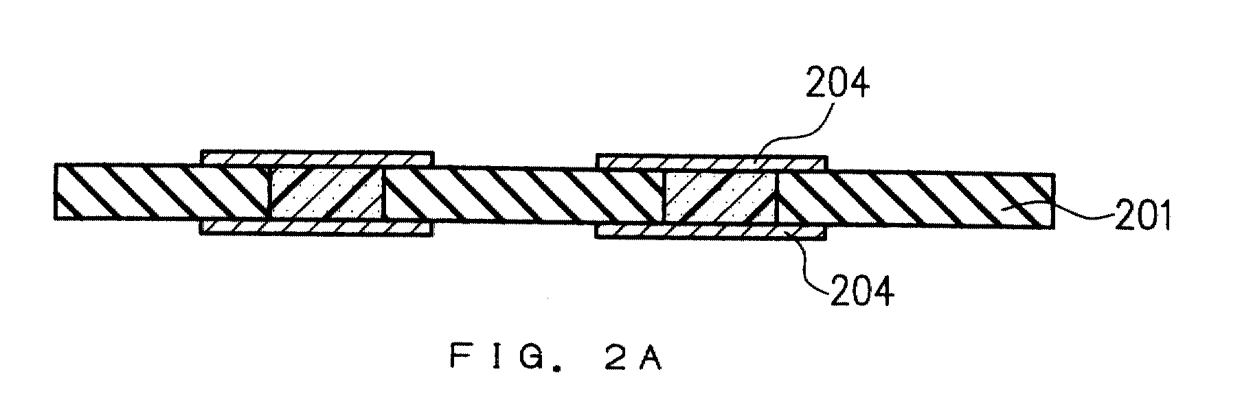
    FIGs. 2A-2D are cross-sectional views to show steps of manufacturing a printed circuit board in Example 2 of the present invention.
    FIGs. 3A and 3B are cross-sectional views to show steps of manufacturing a printed circuit board in Example 3 of the present invention.
    FIGs. 4A-4C are distribution charts to show variations in resistance values of the printed circuit board in Example 1 of the present invention.
    FIG. 5 is a graph to show a relationship between a thickness of a resin layer of the printed circuit board and initial resistance values in Example 1 of the present invention.
    FIG. 6 is a cross sectional view to show a structure of a printed circuit board in Example 4 of the present invention.
    FIG. 7 is a cross sectional view to show a structure of a printed circuit board in Example 5 of the present invention.
    FIG. 8A-8C are cross-sectional views to show steps of manufacturing a printed circuit board in Example 6 of the present invention.
    FIG. 9A and 9B are enlarged views to show parts of the cross-sectional views of FIGs. 8A and 8B.
    FIG. 10 is a partially enlarged cross-sectional view to show that an inorganic filler is mixed with a dielectric substrate shown in FIG. 9B.
    FIG. 11 is a graph to show mechanical strength characteristics of an internal circuit board and of external circuit boards composing the printed circuit board in Example 6 of the present invention.
    FIG. 12A-12G are cross-sectional views to show steps of manufacturing a conventional printed circuit board.
    A first embodiment of the present invention provides a printed circuit board having excellent connection reliability and repair resistance by improving moisture resistance of the printed circuit board as a whole, and the printed circuit board comprises a dielectric substrate with improved mechanical strength such as flexural rigidity. When an inorganic filler is mixed with an epoxy resin composing the dielectric substrate, melting viscosity of the epoxy resin is raised. This will control resin flow occurring at an interface between the dielectric substrate and a metal foil at the time of applying heat and pressure, and prevent the epoxy resin from entering the interface between the metal foil and the conductor. As a result, the conductor is provided with sufficient compression and this leads to stable connection reliability.
    When the inorganic filler has an average particle diameter smaller than that of the conductive filler, dispersion of the conductive filler during application of heat and pressure is controlled. As a result, the conductor is provided with sufficient compression, and stable connection reliability is obtained. Preferably, the average particle diameter of the inorganic filler is 10% to 50% of the average particle diameter of the conductive filler.
    The conductive filler can be a powder of a metal such as gold, silver, copper, aluminum or the like. When the via hole diameter is about 50µm, the conductive filler preferably has an average particle diameter of about 5µm. Preferably, the conductive filler will have an average particle diameter ranging from about 1µm to about 3µm for a via hole having a diameter of about 30µm.
    When the inorganic filler is at least one powder selected from those of SiO2, TiO2, Al2O3, MgO, SiC and AlN, thus obtained printed circuit board will have further improved mechanical strength including flexural rigidity.
    When a content of the inorganic filler ranges from 25 vol.% to 45 vol.%, the melting viscosity is maintained and sufficient compression is applied to the conductor. When the content of the inorganic filler is less than 25 vol.%, sufficient melting viscosity may not be obtained and excessive resin flow may occur. When the content exceeds 45 vol.%, fluidity of the epoxy resin may deteriorate and the conductor cannot be applied with sufficient compression while the adherence is lowered as well. Preferably the content of the inorganic filler ranges from 35 vol.% to 40 vol.%.
    When thickness of the dielectric substrate is smaller than a diameter of via holes formed in the thickness direction of the dielectric substrate, tapering at the time of formation of the via holes by using a laser beam machine or the like can be controlled, and thus, a thin and light-weight printed circuit board can be provided while the rigidity is maintained. Since the conductor will be compressed easily as the dielectric substrate is thinner (the compression rate is raised since the conductor becomes relatively thicker by the thickness of the mold-releasing films), the dielectric substrate is preferably 50µm to 100µm in thickness when each via hole has a diameter ranging from 100µm to 200µm.
    When the dielectric substrate in a pre-preg stage comprises a void, the dielectric substrate will be compressed by the void volume upon application of heat and pressure. As a result, the conductor is applied with sufficient compression and stable connection resistance is obtained.
    A coefficient of thermal expansion (CTE) in the thickness direction of a conductor filled in via holes formed in the thickness direction of the dielectric substrate substantially is equal to the CTE in the thickness direction of the dielectric substrate, distortion caused by a gap in the CTEs can be controlled and stable connection reliability is obtainable even under a circumstance to cause an abrupt change in temperature. Preferably, the CTE of the conductor in the thickness direction is equal to the CTE of the dielectric substrate in the thickness direction.
    The printed circuit board can be a multilayer printed circuit board comprising a laminate of printed circuit boards according to the present invention. Accordingly, the present invention can provide a multilayer printed circuit board having reliable via hole connection.
    When a conductor filled in via holes formed in the thickness direction of the dielectric substrate is substantially uniform in the thickness in the multilayer printed circuit board of the present invention, an excellent impedance property is obtained, and a printed circuit board suitable for a high frequency circuit board can be provided.
    In a case where the conductor is a conductive paste, resin ingredients in the conductive paste will be discharged from the via holes when the conductive paste in the via holes is compressed. As a result, conductive ingredients in the conductive paste are condensed to provide a reliable via hole connection.
    By using a laser beam machine, via holes having a minute diameter in accordance with a minute wiring pattern can be formed easily at a high speed.
    A first manufacturing method in the present invention can provide a double-sided printed circuit board that is excellent in the moisture resistance, connection reliability or repair resistance, and the printed circuit board comprises a dielectric substrate provided with improved mechanical strength such as flexural rigidity.
    When the dielectric substrate is thinned after application of heat and pressure, the conductor can be applied with sufficient compression. For controlling resin flow, it is preferable that the dielectric substrate is thinned by 10% to 15% after application of heat and pressure.
    When the conductor filled in the via holes formed in the thickness direction of the dielectric substrate is thinned after the application of heat and pressure, the conductive ingredients in the conductor are condensed due to sufficient compression, and this leads to a reliable via hole connection. Preferably, the conductor is thinned by 30% to 40% by the application of heat and pressure.
    When the dielectric substrate after being applied with heat and pressure is substantially uniform in thickness in the center and in the periphery, the entire dielectric substrate will be applied with uniform compression at a time of applying heat and pressure, and thus, variation in the connection resistance can be reduced.
    Alternatively, the present invention can provide a rigid, thin, and small multilayer printed circuit board that is provided with excellent reliability and that can form a minute wiring pattern to allow a high density package of a subminiature electronic element or the like. A method of manufacturing the printed circuit board comprises two processes. In a first process, a dielectric substrate of a pre-preg is made of either a glass cloth or a glass nonwoven fabric. The glass cloth or glass nonwoven fabric is impregnated with a thermosetting epoxy resin and filled with a conductor. Metal foils are adhered to this dielectric substrate, and the dielectric substrate is compressed by applying heat and pressure, so that wiring layers of the double-sided printed circuit board are embedded in resin layers on the surfaces of the dielectric substrate and all the conductors become substantially uniform in thickness. In a second process, the metal foils are formed to have a predetermined pattern.
    Alternatively, the present invention can provide a multilayer printed circuit board with excellent reliability in fewer steps at a low cost, and the printed circuit board allows high density package of subminiature electronic elements or the like. A method to manufacture such a printed circuit board comprises preparing either a glass cloth or a glass nonwoven fabric, producing a dielectric substrate of a pre-preg by impregnating the glass cloth or glass nonwoven fabric with a thermosetting epoxy resin and filling with a conductor, sticking the dielectric substrate integrally on surfaces of the plural double-sided printed circuit boards before compressing by application of heat and pressure. As a result, wiring layers of the double-sided printed circuit board are embedded in resin layers on the surfaces of the dielectric substrate and all the conductors become substantially uniform in thickness.
    A second printed circuit board according to the present invention is of a complex type with excellent flexural rigidity and moisture resistance, and this printed circuit board is provided by arranging a glass epoxy resin substrate as an external circuit board having excellent mechanical strength and moisture resistance.
    It is preferred that an aramid nonwoven fabric impregnated with a thermosetting epoxy resin is used for a dielectric substrate of an internal circuit board. As a result, a first interstitial via conductor having a minute diameter can be provided to an arbitrary position on the dielectric substrate so as to provide an any-layer IVH structure. This serves to provide a printed circuit board having a high density wiring.
    Preferably, the external circuit board is made of glass fibers impregnated with an epoxy resin, and the epoxy resin is mixed with an inorganic filler contained in a range from 30 wt% to 70 wt%, and the inorganic filler is at least one powder of SiO2, TiO2, Al2O3, MgO, SiC and AlN, so that the flexural rigidity is improved further and thus, a printed circuit board with good compression property can be obtained.
    A second manufacturing method according to the present invention can provide a complex printed circuit board having excellent flexural strength and moisture resistance.
    Embodiments of the present invention will be explained further by referring to the drawings.
    (Example 1)
    FIG. 1A-1F are cross-sectional views to show steps of a method of manufacturing a double-sided circuit board in Example 1 of the present invention.
    First, a dielectric substrate 102 of a glass epoxy pre-preg was prepared by impregnating a glass cloth with a thermosetting epoxy resin comprising 40 vol.% of SiC fine particles having an average diameter of 2µm. The glass epoxy pre-preg in Example 1 was 130µm in thickness, since the thickness of the glass cloth was 100µm and the thickness of each surface resin layer was 15µm. On both surfaces of the dielectric substrate 102, mold-releasing films 101 (e.g., polyester) were laminated. The lamination was carried out at a temperature about 120°C. As a result, resin layers on the surfaces of the dielectric substrate 102 to which the mold-releasing films 101 were stuck were melted slightly. FIG. 5 is a graph to show the dependence of an initial resistance value on the thickness of the resin layer of the material included in a printed circuit board. Since the initial resistance value is lowered as the resin layer of the material is thinned, the material in Example 1 was determined to be 130µm in thickness. The mold-releasing films used here were polyethylene terephthalate (PET) 19µm in thickness. The glass cloth used for the dielectric substrate can be replaced by a glass nonwoven fabric on which resin layers are formed.
    The fine particles can be an organic filler and/or an inorganic filler. SiC as the inorganic filler can be replaced by SiO2, TiO2, Al2O3, MgO or AlN, while the organic filler can include benzoguanamine, polyamide, polyimide, melamine resin, epoxy resin or the like. Alternatively, the organic filler and the inorganic filler can be used as a mixture.
    As shown in FIG. 1B, via holes 103 were formed at predetermined positions on the dielectric substrate 102 by a laser processing. The via holes formed by the above-mentioned laser beam machine had a diameter of about 100µm. The glass epoxy pre-preg comprises 10 vol.% voids, and diameter of the voids was 3µm.
    Next, the via holes 103 were filled with a conductive paste 104 as shown in FIG. 1C. A screen printer was used for filling by directly printing the conductive paste 104 on the mold-releasing films 101. At this time, vacuum adsorption was performed via, for example, a porous sheet such as Japanese paper from a surface opposite to the printed surface so that resin ingredients contained in the conductive paste 104 in the via holes 103 were absorbed and thus, a content of the conductive ingredients was increased and concentration of the filled conductive ingredients was raised. The mold-releasing films 101 functioned as printing masks and also the films served to prevent contamination of the surfaces of the dielectric substrate 102. An average particle diameter of the conductive filler in the conductive paste was 5µm, and this was larger than a diameter of a void and a diameter of the fine particles.
    As shown in FIG. 1D, the mold-releasing films 101 were peeled off from the surfaces of the dielectric substrate 102. Then, the surfaces of the dielectric substrate 102 were coated with metal foils 105 such as copper foils before application of heat and pressure. The heat and pressure were applied by a vacuum press. This process was carried out for one hour under a condition of a temperature of 200°C, a pressure of 4.9MPa, and a vacuum degree of 5.33×10³Pa (40 Torr).
    As a result of applying heat and pressure under the condition, the dielectric substrate 102 was compressed as shown in FIG. 1E. The dielectric substrate 102 was thinned to 118µm at the center and 116µm in the periphery. The difference in the thickness between the center and the periphery was as small as about 2%, and the compression rate as a whole was about 10%. At this time, the conductive paste 104 in the via holes 103 were compressed as well, and thus, binder ingredients contained in the conductive paste were extruded. This strengthens bonding among the conductive ingredients and also between the conductive ingredients and the metal foils 105, and the conductive substance in the conductive paste 104 was condensed. The compression rate of the conductor at this time was (168-117)×100/168=30.4%. Subsequently, the thermosetting resin composing the dielectric substrate 102 was cured together with the conductive paste 104 by applying heat and pressure. This process was carried out for one hour under a condition of a temperature of 200°C, a pressure of 4.9MPa, and a vacuum degree of 5.33×10³Pa (40 Torr).
    Finally, both the wiring layers 106 on the front and back surfaces of the dielectric substrate 102 were connected electrically with each other by selectively etching the metal foils 105 in a predetermined pattern as shown in FIG. 1F, so that a double-sided circuit board was obtained.
    An average particle diameter of a conductive powder contained in the conductive paste was 5µm in Example 1, and an average particle diameter of the inorganic filler was 40% of that of the conductive powder. The CTE of the conductor in a thickness direction was about 30 ppm/°C while the CTE of the dielectric substrate in the thickness direction was about 20ppm/°C, i.e., CTE of the conductor was larger than that of the dielectric substrate.
    Since the filler has an average diameter larger than that of the fine particles, the fine particles can prevent dispersion of the conductive filler in the resin layers on the surfaces of the dielectric substrate during application of heat and pressure. This helps to apply sufficient compression to the conductor, resulting in a stable connection reliability and excellent moisture absorption. This can prevent peeling of the conductor and the wiring layers, which is caused by abrupt change in temperature at a time of solder dipping or repairing.
    Furthermore, the epoxy resin composing the dielectric substrate was mixed with 40 vol.% of SiC as an inorganic filler having an average diameter of 2µm. FIGs. 4A-4C are distribution diagrams to show variation in resistance values of printed circuit boards. As shown in FIG 4A, the resistance values were varied when the filling amount was 20 vol.%. On the other hands, FIG. 4B shows that the filler of 30 vol.% caused some variation though the distribution was substantially concentrated. The distribution was concentrated further when the filling amount was 40 vol.% as shown in FIG. 4C.
    When the content of the fine particle ranges from 25 vol.% to 45 vol.%, the melting viscosity is maintained while the conductor is applied with sufficient compression, and thus, stable connection reliability is obtained. When the content is less than 25 vol.%, sufficient melting viscosity is not obtained. As a result, excessive resin flow occurs in the resin layers on the surfaces of the dielectric substrate and the conductive filler contained in the conductor is dispersed, so that pressure applied to the conductor will be dispersed as well. Moreover, the dispersed conductive filler can migrate to cause insulation failure. When the content exceeds 45 vol.%, sufficient epoxy resin to provide a desired adherence may not be obtained, and the fluidity of the epoxy resin deteriorates to apply insufficient compression to the conductor. It is more preferable that the content of the fine particle ranges from 30 vol.% to 35 vol.%.
    Accordingly, Example 1 can improve mechanical strengths such as flexural rigidity of a dielectric substrate and provide a printed circuit board having excellent connection reliability and moisture absorption.
    (Example 2)
    FIGs. 2A-2D are cross-sectional views to indicate steps of a method of manufacturing a double-sided circuit board in Example 2 of the present invention.
    First, a core substrate 201 was prepared in the same process as indicated in FIG. 1F of Example 1.
    Next, as shown in FIG. 2B, dielectric substrates 202 shown in FIG. 1C were layered on the both surfaces of the core substrate 201, and metal foils 203 were layered further before application of heat and pressure. The heat and pressure were applied by vacuum heat press. This process was carried out for one hour under a condition of a temperature of 200°C, a pressure of 4.9MPa, and a vacuum degree of 5.33×10³Pa (40 Torr).
    The dielectric substrates 202 were compressed and thinned by the application of heat and pressure, and the wiring layers 204 were embedded in the dielectric substrates 202. The conductive paste 205 also was compressed, and at that time, binder ingredients contained in the conductive paste were extruded. This provided strong bonding among the conductive ingredients and also between the conductive ingredients and the metal foils 203, and thus, the conductive substance in the conductive paste 205 was condensed. Subsequently, the conductive paste 205 and the thermosetting resin composing the dielectric substrates 202 were cured.
    Next, as shown in FIG. 2C, the metal foils 203 were etched selectively to have a predetermined pattern, so that the wiring layers 204 and 206 were connected electrically to provide a completed four-layered circuit board.
    In the last step shown in FIG. 2D, dielectric substrates 207 were layered on both surfaces of the four-layered circuit board. The wiring layer 206 was connected electrically with the wiring layer 208 through steps as shown in FIGs. 2B and 2C, so that a six-layered circuit board was obtained.
    All layers of the six-layered circuit board according to Example 2 were composed of glass epoxy, and laminated integrally. Therefore, compact wiring patterns to allow high density packaging of elements such as a subminiature electronic element can be formed, and the printed circuit board has excellent rigidity, moisture absorption, and repair property.
    (Example 3)
    FIG. 3A and 3B are cross-sectional views to show steps in a method of manufacturing a double-sided printed circuit board according to Example 3 of the present invention.
    As shown in FIG. 3A, three core substrates 301 provided by the step shown in FIG. 1F, and two dielectric substrates 302 provided by the step shown in FIG. 1C were prepared. The respective dielectric substrates 302 were inserted between the core substrates 301 to form a laminate before application of heat and pressure. The heat and pressure were applied by a vacuum heat press. This process was carried out for one hour under a condition of a temperature of 200°C, a pressure of 4.9MPa, and a vacuum degree of 5.33×10³Pa (40 Torr).
    As a result of application of heat and pressure, the dielectric substrates 302 were compressed and thinned as shown in FIG. 3B, and the wiring layers 303 were embedded in the dielectric substrates 302. The conductive paste 304 also was compressed at this time, and the binder ingredients contained in the conductive paste were extruded to strengthen bonding among the conductive ingredients and also between the conductive ingredients and the wiring layers 303, and thus, the conductive substance in the conductive paste 304 was condensed. Later, the conductive paste 304 and the thermosetting resin composing the dielectric substrates 302 were cured by the application of heat and pressure, and the wiring layers 303 were connected electrically, so that a six-layered circuit board was obtained.
    All layers of a six-layered circuit board according to Example 3 are composed of glass epoxy, and laminated integrally. Therefore, compact wiring patterns to allow high density packaging of elements such as a subminiature electronic element can be formed with fewer steps at a low cost, and the printed circuit board has excellent rigidity, moisture absorption, and repair property.
    (Example 4)
    FIG. 6 shows a printed circuit board in Example 4 of the present invention. An external circuit board 6 comprising dielectric substrates 5 of a glass epoxy resin was manufactured in accordance with Example 1. An internal circuit board 4 in this example has a three-layered any-layer IVH structure having dielectric substrates 3 of an aramid epoxy resin in which a first interstitial via conductor 1a and a first wiring pattern 2a were formed. On both surfaces of the internal circuit board 4, the external circuit boards 6 comprising dielectric substrates 5 of a glass epoxy resin having a second wiring pattern 2 on outermost layers connected with the first wiring pattern 2a of the internal circuit board 4 through a second interstitial via conductor 1b were arranged. A conductive paste filled in the via holes was compressed to be the second interstitial via conductor 1b when the external circuit boards 6 were laminated on the internal circuit board 4. The thus formed second interstitial via conductor 1b had sufficient conductivity.
    (Example 5)
    FIG. 7 shows a printed circuit board in Example 5 of the present invention. The printed circuit board is same as that of Example 4 except that the internal circuit board 4 is a double-sided circuit board comprising a dielectric substrate 3 of an aramid epoxy resin. The printed circuit board had a structure similar to that of Example 1 except for the above-identified matter.
    (Example 6)
    In the following, a method of manufacturing a printed circuit board in Example 6 will be described by referring to FIGs. 8A-8C where some of the elements common to those of FIG. 6.
    FIG. 8A shows a structure of a printed circuit board according to Example 6. An internal circuit board 4 has an any-layer IVH structure in which first wiring patterns 2a are connected with each other by a first interstitial via conductor 1a. On both surfaces of the internal circuit board 4, dielectric substrates 5 comprising a glass epoxy resin in a pre-preg stage are arranged, and the dielectric substrates 5 are filled with a conductive paste 7 by printing or the like. The conductive paste 7 comprises a conductive powder such as silver or copper as a main ingredient for forming a second interstitial via conductor 1b. Copper foils 8 are arranged further on the surfaces.
    Subsequently, as shown in FIG. 8B, the entire body is compressed and laminated by applying heat and pressure from both sides by using a press such as a mold. As a result, the first wiring patterns 2a formed in the outermost layers of the internal circuit board 4 are forced into the surface layers of the glass epoxy resin dielectric substrates 5 that have been in a pre-preg stage before the compression, and at the same time, the conductive paste 7 provided in the glass epoxy resin dielectric substrates 5 is compressed to have conductivity so that the conductive paste 7 becomes the second interstitial via conductor 1b to connect the first wiring patterns 2a and the copper foils 8 electrically. At this time, the copper foils 8 are adhered strongly through the epoxy resin layers flowing on the surfaces of the dielectric substrates 5.
    Next, as shown in FIG. 8C, the copper foils 8 as outermost layers adhered to the surfaces are patterned selectively by an ordinary photolithography in order to form second wiring patterns 2b, so that the first wiring patterns 2a and the second wiring patterns 2b are connected to each other through the first interstitial via conductor 1a and the second interstitial via conductor 1b in order to provide a complex printed circuit board having a multilayer structure.
    FIG. 9A is a magnified view of a part of the internal circuit board 4 concerning a manufacturing method shown in FIG. 8A, in which a dielectric substrate 5 and a copper foil 8 are laminated. The dielectric substrate 5 shown in FIG. 9A comprises a glass epoxy resin in a pre-preg stage, in which glass fibers 5a aggregate in the inner layer of the dielectric substrate 5 and epoxy resin 5b is retained on the surface of the dielectric substrate 5.
    Therefore, the dielectric substrate 5, the internal circuit board 4 and the copper foil 8 are arranged as shown in FIG. 9A before applying heat and pressure from both sides, so that the wiring pattern 2a of the internal circuit board 4 is forced into the epoxy resin 5b retained on the surface of the dielectric substrate 5.
    At the same time, the conductive paste 7 filled in the via holes in the dielectric substrate 5 is compressed to decrease the initial thickness of t1 to t2, so that a second interstitial via conductor 1b having a low resistance is formed to allow electrical connection between the copper foil 8 and the first wiring pattern 2a of the internal circuit board 4.
    FIG. 10 shows an external circuit board 10 in which a dielectric substrate similar to that of FIGs. 9A and 9B comprises a glass epoxy resin mixed with 30 wt% to 70 wt% of at least one inorganic filler 9 comprising powders of SiO2, TiO2, Al2O3, MgO, SiC, AlN or the like. Addition of the inorganic filler 9 raises the viscosity of the epoxy resin, and this can prevent the dielectric epoxy resin from entering the interface between the first wiring pattern 2a or the copper foil 8 and the conductive paste. As a result, the electric connection reliability is improved, and the mechanical strength of the printed circuit board can be improved. The conductive paste is applied with heat and pressure to be the second wiring pattern 1b.
    Since the CTE direction of the dielectric substrate in the thickness can be decreased to a range from 20ppm to 30ppm by mixing the inorganic filler, the value approaches the CTE of an interstitial via conductor (about 17ppm), and this improves connection reliability between the wiring pattern and the interstitial via conductor. Furthermore, a coefficient of thermal expansion in the face direction of the printed circuit board can be decreased as well, and thus, the connection reliability can be improved at a time of packaging a semiconductor chip.
    FIG. 11 is a graph to show a measurement result concerning flexural rigidities of an internal circuit board 4, an external circuit board 6 and an external circuit board 10 comprising an inorganic filler of a printed circuit board according to the present invention. The external circuit board 6 made of a glass epoxy resin has a flexural rigidity higher than that of the internal circuit board 4 comprising an aramid epoxy resin. The external circuit board 10 additionally comprising an inorganic filler has an even higher flexural rigidity.
    A printed circuit board according to the present invention comprises an external circuit board 6 or 10 comprising a glass epoxy resin arranged on both sides of an internal circuit board 4 comprising an aramid epoxy resin. Such a printed circuit board can have excellent packaging reliability for respective electronic elements, and also repair property and moisture resistance for the elements.
    The mechanical strength cannot be expected to improve further when the content of the inorganic filler is less than 30 wt%. On the other hand, when the content exceeds 70wt%, the epoxy resin will have inferior fluidity, and impregnating ability with respect to the glass fibers deteriorates. As a result, it will be difficult to obtain a homogeneous glass epoxy resin dielectric substrate.

    Claims (22)

    1. A printed circuit board comprising a dielectric substrate having a via hole formed in a thickness direction of the dielectric substrate and filled with a conductor containing a conductive filler, the dielectric substrate having wiring layers on both surfaces, and the wiring layers being formed to have a predetermined pattern and connected electrically with each other by the conductor, wherein
         the dielectric substrate comprises a glass cloth or a glass nonwoven fabric impregnated with a thermosetting epoxy resin mixed with fine particles, and the conductive filler in the conductor has an average particle diameter larger than an average diameter of the fine particles.
    2. The printed circuit board according to claim 1, wherein the fine particles are at least one inorganic filler selected from powders of SiO2, TiO2, Al2O3, MgO, SiC and AlN.
    3. The printed circuit board according to claim 1 or 2, wherein the conductor filled in the via hole formed in the thickness direction of the dielectric substrate has a coefficient of thermal expansion larger than a coefficient of thermal expansion of the dielectric substrate in the thickness direction.
    4. The printed circuit board according to any of claims 1 to 3, wherein a content of the fine particles ranges from 25 vol.% to 45 vol.%.
    5. The printed circuit board according to any of claims 1 to 4, wherein the thickness of the dielectric substrate is smaller than a diameter of the via hole formed in the thickness direction of the dielectric substrate.
    6. The printed circuit board according to any of claims 1 to 5, wherein the dielectric substrate in a pre-preg stage comprises a void.
    7. The printed circuit board according to any of claims 1 to 6, comprising a single printed circuit board.
    8. The printed circuit board according to any of claims 1 to 7, comprising a multilayer printed circuit board of a laminate of a plurality of the printed circuit boards.
    9. The printed circuit board according to claim 8, wherein the conductor filled in the via hole formed in the thickness direction of the dielectric substrate of the multilayer printed circuit board has a substantially uniform thickness.
    10. The printed circuit board according to any of claims 1 to 9, wherein
      the dielectric substrate comprises external circuit boards prepared by impregnating either glass cloths or glass nonwoven fabrics with a thermosetting epoxy resin mixed with fine particles, and an internal circuit board having at least two layers of wiring patterns connected electrically with each other by an interstitial via conductor provided with conductivity by compression, and
      the external circuit boards comprise wiring patterns connected electrically with the wiring patterns of the internal circuit board.
    11. The printed circuit board according to claim 10, wherein the internal circuit board is a dielectric substrate prepared by impregnating an aramid nonwoven fabric with a thermosetting epoxy resin.
    12. The printed circuit board according to claim 10, wherein plural external circuit boards are formed on at least one surface of the internal circuit board.
    13. A method of manufacturing a printed circuit board according to any of claims 1 to 9, comprising:
      preparing a dielectric substrate of a pre-preg formed by impregnating a glass cloth or a glass nonwoven fabric with a thermosetting epoxy resin mixed with fine particles,
      coating both surfaces of the dielectric substrate with mold-releasing films and subsequently forming a via hole,
      filling in the via hole with a conductor containing a conductive filler having an average particle diameter larger than an average diameter of the fine particles,
      peeling the mold-releasing films and layering metal foils on the surfaces of the dielectric substrate,
      compressing the dielectric substrate having the metal foils by applying heat and pressure in order to adhere the dielectric substrate and the metal foils and to connect electrically the metal foils with each other, and
      forming the metal foils to have a predetermined pattern.
    14. The method of manufacturing a printed circuit board according to claim 13, wherein the resin layers on the surfaces of the pre-preg have a thickness ranging from 5µm to 25µm.
    15. The method of manufacturing a printed circuit board according to claim 13, wherein the dielectric substrate in a pre-preg stage comprises a void.
    16. The method of manufacturing a printed circuit board according to any of claims 13 to 15, wherein the void has a diameter smaller than a diameter of the conductive filler in the conductor.
    17. The method of manufacturing a printed circuit board according to any of claims 13 to 16, wherein the dielectric material is thinned by applying heat and pressure.
    18. The method of manufacturing a printed circuit board according to any of claims 13 to 16, wherein the conductor filled in the via hole formed in the thickness direction of the dielectric substrate is thinned by applying heat and pressure.
    19. The method of manufacturing a printed circuit board according to any of claims 13 to 18, wherein the dielectric substrate has a substantially uniform thickness in the center and in the periphery after application of heat and pressure.
    20. A method of manufacturing a printed circuit board, comprising:
      filling a conductor in a dielectric substrate composed of a pre-preg of a glass cloth or a glass nonwoven fabric impregnated with a thermosetting epoxy resin mixed with fine particles,
      layering the dielectric substrate and metal foils onto both surfaces of a printed circuit board prepared in accordance with any of claims 13 to 19,
      compressing the printed circuit board by applying heat and pressure so as to embed wiring layers of the printed circuit board in the resin layers on the surfaces of the dielectric substrate, and
      forming the metal foils to have a predetermined pattern.
    21. A method of manufacturing a printed circuit board, comprising:
      forming a plurality of double-sided printed circuit boards according to any of claims 13 to 19,
      filling a conductor in a dielectric substrate composed of a pre-preg of a glass cloth or a glass nonwoven fabric impregnated with a thermosetting epoxy resin mixed with fine particles,
      layering the dielectric substrate between the double-sided printed circuit boards,
      compressing the printed circuit board by applying heat and pressure so as to embed the wiring layers of the double-sided printed circuit board in the resin layers on the surfaces of the dielectric substrate,
      with all the conductors having substantially same thickness.
    22. A method of manufacturing a printed circuit board according to any of claims 10 to 12, comprising:
      preparing an internal circuit board that can be compressed and has at least two layers of first wiring patterns connected with each other by first interstitial via conductors,
      preparing glass epoxy resin dielectric substrates in a pre-preg stage by forming via holes in which a conductive paste for forming second interstitial via conductors is filled,
      arranging the glass epoxy resin dielectric substrates on both surfaces of the internal circuit board,
      arranging copper foils on outer surfaces of the respective glass epoxy resin dielectric substrates,
      applying heat and pressure from outside of the two copper foils to the internal circuit board and the glass epoxy resin dielectric substrates in a pre-preg stage so as to force the wiring patterns protruding from the surfaces of the internal circuit board into the glass epoxy resin dielectric substrate in a pre-preg stage and at the same time to compress the conductive paste provided in the glass epoxy resin dielectric substrates for connecting electrically the outermost copper foils and the first wiring patterns in the internal circuit board, and subsequently
      etching the copper foils selectively to form second wiring patterns and so as to configure external circuit boards.
    EP01113580A 2000-06-14 2001-06-13 Printed circuit board and method of manufacturing the same Withdrawn EP1164823A3 (en)

    Applications Claiming Priority (4)

    Application Number Priority Date Filing Date Title
    JP2000177936 2000-06-14
    JP2000177936 2000-06-14
    JP2001105446 2001-04-04
    JP2001105446 2001-04-04

    Publications (2)

    Publication Number Publication Date
    EP1164823A2 true EP1164823A2 (en) 2001-12-19
    EP1164823A3 EP1164823A3 (en) 2003-09-10

    Family

    ID=26593893

    Family Applications (1)

    Application Number Title Priority Date Filing Date
    EP01113580A Withdrawn EP1164823A3 (en) 2000-06-14 2001-06-13 Printed circuit board and method of manufacturing the same

    Country Status (5)

    Country Link
    US (2) US6753483B2 (en)
    EP (1) EP1164823A3 (en)
    KR (1) KR100475712B1 (en)
    CN (1) CN1201642C (en)
    TW (1) TWI242398B (en)

    Cited By (7)

    * Cited by examiner, † Cited by third party
    Publication number Priority date Publication date Assignee Title
    EP2150096A4 (en) * 2007-05-14 2013-02-20 Ibiden Co Ltd CONNECTION TABLE AND METHOD FOR MANUFACTURING THE SAME
    EP2154939A4 (en) * 2007-05-14 2013-02-20 Ibiden Co Ltd Wiring board and method of manufacturing the same
    GB2488265B (en) * 2009-12-17 2014-04-30 Intel Corp Substrate for integrated circuit devices including multi-layer glass core and methods of making the same
    US9642248B2 (en) 2012-09-24 2017-05-02 Intel Corporation Microelectronic structures having laminated or embedded glass routing structures for high density packaging
    US9686861B2 (en) 2009-12-17 2017-06-20 Intel Corporation Glass core substrate for integrated circuit devices and methods of making the same
    US9793201B2 (en) 2012-03-07 2017-10-17 Intel Corporation Glass clad microelectronic substrate
    CN115776766A (en) * 2021-09-08 2023-03-10 鹏鼎控股(深圳)股份有限公司 Circuit board connecting structure and manufacturing method thereof

    Families Citing this family (72)

    * Cited by examiner, † Cited by third party
    Publication number Priority date Publication date Assignee Title
    USRE40947E1 (en) * 1997-10-14 2009-10-27 Ibiden Co., Ltd. Multilayer printed wiring board and its manufacturing method, and resin composition for filling through-hole
    US6753483B2 (en) * 2000-06-14 2004-06-22 Matsushita Electric Industrial Co., Ltd. Printed circuit board and method of manufacturing the same
    JPWO2003009656A1 (en) * 2001-07-18 2004-11-11 松下電器産業株式会社 Circuit forming substrate manufacturing method and circuit forming substrate
    US20040145577A1 (en) * 2001-07-27 2004-07-29 Hiroshi Yajima Input device and its manufacturing method
    JP3969192B2 (en) * 2002-05-30 2007-09-05 株式会社デンソー Manufacturing method of multilayer wiring board
    JP2004216385A (en) * 2003-01-09 2004-08-05 Hitachi Via Mechanics Ltd Laser drilling method
    TW200505304A (en) * 2003-05-20 2005-02-01 Matsushita Electric Industrial Co Ltd Multilayer circuit board and method for manufacturing the same
    US20050014035A1 (en) * 2003-07-16 2005-01-20 Matsushita Electric Industrial Co., Ltd. Prepreg for printed wiring board, printed wiring board using the prepreg and method for manufacturing the printed wiring board, and multilayer printed wiring board and method for manufacturing the multilayer printed wiring board
    US7547975B2 (en) * 2003-07-30 2009-06-16 Tdk Corporation Module with embedded semiconductor IC and method of fabricating the module
    US6982206B1 (en) * 2003-10-02 2006-01-03 Lsi Logic Corporation Mechanism for improving the structural integrity of low-k films
    US20050124197A1 (en) * 2003-12-04 2005-06-09 Matsushita Electric Industrial Co., Ltd. Circuit board and method for manufacturing the same, semiconductor package, component built-in module and board for electronic equipment
    WO2005055680A1 (en) * 2003-12-05 2005-06-16 The Commonwealth Of Australia Method of manufacturing an electrical component
    WO2005073621A1 (en) * 2004-01-29 2005-08-11 Matsushita Electric Industrial Co., Ltd. Led illumination light source
    JP4020891B2 (en) * 2004-06-14 2007-12-12 三洋電機株式会社 Device mounting substrate manufacturing method
    US20060000542A1 (en) * 2004-06-30 2006-01-05 Yongki Min Metal oxide ceramic thin film on base metal electrode
    TW200618705A (en) * 2004-09-16 2006-06-01 Tdk Corp Multilayer substrate and manufacturing method thereof
    US7560215B2 (en) * 2004-10-04 2009-07-14 Hewlett-Packard Development Company, L.P. Printed circuit board printing system and method using liquid electrophotographic printing
    US7290315B2 (en) * 2004-10-21 2007-11-06 Intel Corporation Method for making a passive device structure
    US20060099803A1 (en) * 2004-10-26 2006-05-11 Yongki Min Thin film capacitor
    US20060091495A1 (en) * 2004-10-29 2006-05-04 Palanduz Cengiz A Ceramic thin film on base metal electrode
    JP4608297B2 (en) * 2004-12-06 2011-01-12 インターナショナル・ビジネス・マシーンズ・コーポレーション Manufacturing method of multilayer wiring board
    JP4617941B2 (en) * 2005-03-17 2011-01-26 パナソニック株式会社 Method for manufacturing circuit-formed substrate
    US20060220177A1 (en) * 2005-03-31 2006-10-05 Palanduz Cengiz A Reduced porosity high-k thin film mixed grains for thin film capacitor applications
    US7375412B1 (en) * 2005-03-31 2008-05-20 Intel Corporation iTFC with optimized C(T)
    US7629269B2 (en) * 2005-03-31 2009-12-08 Intel Corporation High-k thin film grain size control
    TWI275332B (en) * 2005-04-26 2007-03-01 Phoenix Prec Technology Corp Method for fabricating interlayer conducting structure of circuit board
    US7349196B2 (en) * 2005-06-17 2008-03-25 Industrial Technology Research Institute Composite distributed dielectric structure
    US7453144B2 (en) * 2005-06-29 2008-11-18 Intel Corporation Thin film capacitors and methods of making the same
    US7650694B2 (en) * 2005-06-30 2010-01-26 Intel Corporation Method for forming multilayer substrate
    JP4535002B2 (en) 2005-09-28 2010-09-01 Tdk株式会社 Semiconductor IC-embedded substrate and manufacturing method thereof
    US7381587B2 (en) * 2006-01-04 2008-06-03 Endicott Interconnect Technologies, Inc. Method of making circuitized substrate
    US20100224395A1 (en) * 2006-03-28 2010-09-09 Panasonic Corporation Multilayer wiring board and its manufacturing method
    JP4253334B2 (en) * 2006-07-12 2009-04-08 株式会社東芝 Two-dimensional array type ultrasonic probe
    US8148647B2 (en) * 2006-08-23 2012-04-03 Mitsubishi Electric Corporation Printed circuit board and method of manufacturing the same
    JP2008071812A (en) * 2006-09-12 2008-03-27 Fujikura Ltd Board to board connection structure
    US8669480B2 (en) * 2007-05-17 2014-03-11 Ibiden Co., Ltd. Wiring board and method of manufacturing wiring board
    US8648263B2 (en) * 2007-05-17 2014-02-11 Ibiden Co., Ltd. Wiring board and method of manufacturing wiring board
    US7982137B2 (en) * 2007-06-27 2011-07-19 Hamilton Sundstrand Corporation Circuit board with an attached die and intermediate interposer
    KR100872574B1 (en) 2007-07-04 2008-12-08 삼성전기주식회사 Multilayer printed circuit board and its manufacturing method
    US8035983B2 (en) * 2007-07-17 2011-10-11 Ibiden Co., Ltd. Wiring board and method of manufacturing wiring board
    US8258620B2 (en) * 2007-08-10 2012-09-04 Sanyo Electric Co., Ltd. Circuit device, method of manufacturing the circuit device, device mounting board and semiconductor module
    JP2009054621A (en) * 2007-08-23 2009-03-12 Panasonic Corp Multilayer wiring board
    CN101207312B (en) * 2007-10-24 2012-01-11 苏州巨峰电气绝缘系统股份有限公司 Interface strap for generator coil die stamping insulation and production method thereof
    CN101472404B (en) * 2007-12-25 2011-12-07 富葵精密组件(深圳)有限公司 Multi-layer circuit board and manufacturing method thereof
    JP2009170753A (en) * 2008-01-18 2009-07-30 Panasonic Corp Multilayer printed wiring board and mounting body using the same
    EP2259666A4 (en) * 2008-03-27 2011-09-07 Ibiden Co Ltd PRINTED CIRCUIT BOARD COMPRISING INTEGRATED ELECTRONIC COMPONENTS, AND METHOD FOR MANUFACTURING THE SAME
    KR101284376B1 (en) * 2009-01-27 2013-07-09 파나소닉 주식회사 Method of mounting semiconductor chips, semiconductor device obtained using the method, method of connecting semiconductor chips, and three-dimensional structure, on the surface of which wiring is provided and fabrication method thereof
    JP2011060892A (en) * 2009-09-08 2011-03-24 Renesas Electronics Corp Electronic device and method for manufacturing the same
    KR20110038521A (en) * 2009-10-08 2011-04-14 엘지이노텍 주식회사 Printed circuit board and manufacturing method thereof
    JP5578962B2 (en) * 2010-06-24 2014-08-27 新光電気工業株式会社 Wiring board
    CN101976716A (en) * 2010-10-21 2011-02-16 光颉科技股份有限公司 Method of conducting electricity through substrate holes
    KR20130077177A (en) * 2011-12-29 2013-07-09 삼성전기주식회사 Power inductor and manufacturing method for the same
    US20130322029A1 (en) * 2012-05-30 2013-12-05 Dror Hurwitz Multilayer electronic structure with integral faraday shielding
    JP6177639B2 (en) * 2013-09-20 2017-08-09 日本メクトロン株式会社 Multilayer printed wiring board manufacturing method and multilayer printed wiring board
    WO2015141004A1 (en) * 2014-03-20 2015-09-24 富士通株式会社 Multilayer circuit board, semiconductor device, and multilayer circuit board manufacturing method
    KR102268385B1 (en) * 2014-08-14 2021-06-23 삼성전기주식회사 Printed circuit board and method of manufacturing the same
    JP2016219452A (en) * 2015-05-14 2016-12-22 富士通株式会社 Multilayer substrate and method for manufacturing multilayer substrate
    KR102412612B1 (en) * 2015-08-28 2022-06-23 삼성전자주식회사 board for package and prepreg
    CN105721749B (en) * 2016-02-24 2020-07-24 宁波舜宇光电信息有限公司 Camera module, electric support and circuit board assembly thereof and manufacturing method
    DE102016209227A1 (en) * 2016-05-27 2017-11-30 Volkswagen Aktiengesellschaft Arrangement for the electrical connection of a cable to an electrical consumer
    JP6627666B2 (en) * 2016-07-07 2020-01-08 株式会社オートネットワーク技術研究所 Circuit board and electrical junction box
    JP6751910B2 (en) * 2016-10-05 2020-09-09 パナソニックIpマネジメント株式会社 Manufacturing method of multi-layer printed wiring board and multi-layer printed wiring board
    CN110798977B (en) * 2018-08-01 2021-03-23 鹏鼎控股(深圳)股份有限公司 Thin antenna circuit board and manufacturing method thereof
    US11938688B2 (en) * 2018-12-18 2024-03-26 Resonac Corporation Laminate, printed wiring board, semiconductor package, and method for manufacturing laminate
    JP7125547B2 (en) 2018-12-29 2022-08-24 深南電路股▲ふん▼有限公司 Printed circuit board that can be assembled in various ways and its manufacturing method
    JP7121294B2 (en) 2019-09-10 2022-08-18 日亜化学工業株式会社 Method for manufacturing light emitting device
    JP7444084B2 (en) * 2021-01-14 2024-03-06 三菱電機株式会社 semiconductor equipment
    US20230317773A1 (en) * 2022-04-01 2023-10-05 Intel Corporation Technologies for low-leakage on-chip capacitors
    US20230389183A1 (en) * 2022-05-26 2023-11-30 Steering Solutions Ip Holding Corporation Non-symmetric single circuit board assembly with polytronics dielectric material
    US12439513B2 (en) 2023-04-04 2025-10-07 Advanced Chip And Circuit Materials, Inc. Use of inorganic thin non-woven dielectrics in printed circuit boards
    CN116456632B (en) * 2023-06-15 2023-08-25 广州添利电子科技有限公司 Pressing manufacturing method of high-rise PCB
    WO2026043099A1 (en) * 2024-08-19 2026-02-26 엘지이노텍 주식회사 Circuit board and semiconductor package comprising same

    Family Cites Families (29)

    * Cited by examiner, † Cited by third party
    Publication number Priority date Publication date Assignee Title
    JPH0834348B2 (en) 1990-01-24 1996-03-29 新神戸電機株式会社 Manufacturing method of multilayer printed wiring board
    CA2060709C (en) * 1991-02-08 1996-06-04 Kiyotaka Komori Glass fiber forming composition, glass fibers obtained from the composition and substrate for circuit board including the glass fibers as reinforcing material
    JP2733160B2 (en) 1991-06-18 1998-03-30 松下電工株式会社 Circuit board
    DE69307944T2 (en) * 1992-04-13 1997-06-26 Mitsubishi Gas Chemical Co Process for the production of substrates for printed circuits
    JP2601128B2 (en) * 1992-05-06 1997-04-16 松下電器産業株式会社 Method of manufacturing circuit forming substrate and circuit forming substrate
    JP3146712B2 (en) 1993-01-12 2001-03-19 松下電器産業株式会社 Double-sided printed circuit board and method of manufacturing the same
    JP3087152B2 (en) * 1993-09-08 2000-09-11 富士通株式会社 Method for manufacturing resin film multilayer circuit board
    EP0645950B1 (en) * 1993-09-21 1998-09-02 Matsushita Electric Industrial Co., Ltd. Connecting member of a circuit substrate and method of manufacturing multilayer circuit substrates by using the same
    CN1044762C (en) * 1993-09-22 1999-08-18 松下电器产业株式会社 Printed circuit board and manufacturing method thereof
    JP2591447B2 (en) 1993-10-20 1997-03-19 松下電器産業株式会社 Multilayer substrate and manufacturing method thereof
    JP4077888B2 (en) * 1995-07-21 2008-04-23 株式会社東芝 Ceramic circuit board
    AU7264696A (en) 1995-10-10 1997-04-30 Allied-Signal Inc. Laminates having improved dielectric properties
    JP3440174B2 (en) 1995-11-24 2003-08-25 松下電器産業株式会社 Multilayer printed wiring board and method of manufacturing the same
    US5707893A (en) * 1995-12-01 1998-01-13 International Business Machines Corporation Method of making a circuitized substrate using two different metallization processes
    JP3197213B2 (en) * 1996-05-29 2001-08-13 松下電器産業株式会社 Printed wiring board and method of manufacturing the same
    JP3219692B2 (en) 1996-06-26 2001-10-15 株式会社東芝 refrigerator
    JP3241605B2 (en) 1996-09-06 2001-12-25 松下電器産業株式会社 Wiring board manufacturing method and wiring board
    JPH10107445A (en) * 1996-09-26 1998-04-24 Kyocera Corp Multilayer wiring board and method of manufacturing the same
    US6143116A (en) * 1996-09-26 2000-11-07 Kyocera Corporation Process for producing a multi-layer wiring board
    TW342578B (en) 1996-09-26 1998-10-11 Toray Industries Photosensitive ceramic blank sheet, ceramic package and process for producing the same
    JPH10135591A (en) 1996-10-29 1998-05-22 Matsushita Electric Ind Co Ltd Thermal conductive substrate and thermal conductive wiring substrate
    JPH10265270A (en) 1996-12-11 1998-10-06 Toray Ind Inc Photosensitive ceramic composition
    JP3961092B2 (en) 1997-06-03 2007-08-15 株式会社東芝 Composite wiring board, flexible substrate, semiconductor device, and method of manufacturing composite wiring board
    JP3889856B2 (en) * 1997-06-30 2007-03-07 松下電器産業株式会社 Method for manufacturing printed wiring board with protruding electrodes
    TW410534B (en) * 1997-07-16 2000-11-01 Matsushita Electric Industrial Co Ltd Wiring board and production process for the same
    SG86345A1 (en) * 1998-05-14 2002-02-19 Matsushita Electric Industrial Co Ltd Circuit board and method of manufacturing the same
    CA2364918C (en) * 1999-03-23 2009-04-14 Circuit Foil Luxembourg Trading S.A.R.L. Method for manufacturing a multilayer printed circuit board and composite foil for use therein
    US6753483B2 (en) * 2000-06-14 2004-06-22 Matsushita Electric Industrial Co., Ltd. Printed circuit board and method of manufacturing the same
    US7078816B2 (en) * 2004-03-31 2006-07-18 Endicott Interconnect Technologies, Inc. Circuitized substrate

    Cited By (11)

    * Cited by examiner, † Cited by third party
    Publication number Priority date Publication date Assignee Title
    EP2150096A4 (en) * 2007-05-14 2013-02-20 Ibiden Co Ltd CONNECTION TABLE AND METHOD FOR MANUFACTURING THE SAME
    EP2154939A4 (en) * 2007-05-14 2013-02-20 Ibiden Co Ltd Wiring board and method of manufacturing the same
    GB2488265B (en) * 2009-12-17 2014-04-30 Intel Corp Substrate for integrated circuit devices including multi-layer glass core and methods of making the same
    US9420707B2 (en) 2009-12-17 2016-08-16 Intel Corporation Substrate for integrated circuit devices including multi-layer glass core and methods of making the same
    US9686861B2 (en) 2009-12-17 2017-06-20 Intel Corporation Glass core substrate for integrated circuit devices and methods of making the same
    US9761514B2 (en) 2009-12-17 2017-09-12 Intel Corporation Substrate for integrated circuit devices including multi-layer glass core and methods of making the same
    US10070524B2 (en) 2009-12-17 2018-09-04 Intel Corporation Method of making glass core substrate for integrated circuit devices
    US9793201B2 (en) 2012-03-07 2017-10-17 Intel Corporation Glass clad microelectronic substrate
    US9642248B2 (en) 2012-09-24 2017-05-02 Intel Corporation Microelectronic structures having laminated or embedded glass routing structures for high density packaging
    US10008452B2 (en) 2012-09-24 2018-06-26 Intel Corporation Microelectronic structures having laminated or embedded glass routing structures for high density packaging
    CN115776766A (en) * 2021-09-08 2023-03-10 鹏鼎控股(深圳)股份有限公司 Circuit board connecting structure and manufacturing method thereof

    Also Published As

    Publication number Publication date
    US20040089471A1 (en) 2004-05-13
    US6753483B2 (en) 2004-06-22
    US20010052425A1 (en) 2001-12-20
    CN1201642C (en) 2005-05-11
    CN1336789A (en) 2002-02-20
    KR100475712B1 (en) 2005-03-10
    KR20010112110A (en) 2001-12-20
    US7155820B2 (en) 2007-01-02
    TWI242398B (en) 2005-10-21
    EP1164823A3 (en) 2003-09-10

    Similar Documents

    Publication Publication Date Title
    US6753483B2 (en) Printed circuit board and method of manufacturing the same
    US7198996B2 (en) Component built-in module and method for producing the same
    JP2601128B2 (en) Method of manufacturing circuit forming substrate and circuit forming substrate
    US7091593B2 (en) Circuit board with built-in electronic component and method for manufacturing the same
    JPH1145955A (en) Element built-in multilayer wiring board and method of manufacturing the same
    JPH09321399A (en) Printed wiring board and method of manufacturing the same
    JP2005072328A (en) Multilayer wiring board
    US20030137815A1 (en) Printed wiring board and method of manufacturing the same
    JP2002368364A (en) Printed wiring board and manufacturing method thereof
    JPH1174625A (en) Wiring board and manufacturing method thereof
    JP2005093556A (en) Printed wiring board and manufacturing method thereof
    JP3440174B2 (en) Multilayer printed wiring board and method of manufacturing the same
    JP2001015872A (en) Insulating sheet for wiring board and method for manufacturing wiring board using the same
    JP4863543B2 (en) Conductive paste and method for manufacturing wiring board using the same
    JPH10107445A (en) Multilayer wiring board and method of manufacturing the same
    JPH11103165A (en) Multilayer wiring board and method of manufacturing the same
    JP3728059B2 (en) Multilayer wiring board
    JP4632514B2 (en) Wiring board and manufacturing method thereof
    JPH1117295A (en) Method of manufacturing prepreg for circuit board, prepreg for circuit board, and method of manufacturing circuit board using prepreg for circuit board
    JP2004356308A (en) Insulating layer for wiring board, wiring board using the same, and method of manufacturing the same
    JP3786894B2 (en) Wiring board and manufacturing method thereof
    JPH1034806A (en) Laminate material and laminate
    JPH1051089A (en) Wiring board and method of manufacturing the same
    JP2002252465A (en) Multilayer wiring board and manufacturing method thereof
    JP2003283087A (en) Printed wiring board and method of manufacturing the same

    Legal Events

    Date Code Title Description
    PUAI Public reference made under article 153(3) epc to a published international application that has entered the european phase

    Free format text: ORIGINAL CODE: 0009012

    AK Designated contracting states

    Kind code of ref document: A2

    Designated state(s): AT BE CH CY DE DK ES FI FR GB GR IE IT LI LU MC NL PT SE TR

    AX Request for extension of the european patent

    Free format text: AL;LT;LV;MK;RO;SI

    PUAL Search report despatched

    Free format text: ORIGINAL CODE: 0009013

    AK Designated contracting states

    Kind code of ref document: A3

    Designated state(s): AT BE CH CY DE DK ES FI FR GB GR IE IT LI LU MC NL PT SE TR

    AX Request for extension of the european patent

    Extension state: AL LT LV MK RO SI

    17P Request for examination filed

    Effective date: 20031015

    AKX Designation fees paid

    Designated state(s): DE FR GB

    STAA Information on the status of an ep patent application or granted ep patent

    Free format text: STATUS: THE APPLICATION HAS BEEN WITHDRAWN

    18W Application withdrawn

    Effective date: 20070615