JP4617941B2 - Method for manufacturing circuit-formed substrate - Google Patents
Method for manufacturing circuit-formed substrate Download PDFInfo
- Publication number
- JP4617941B2 JP4617941B2 JP2005076815A JP2005076815A JP4617941B2 JP 4617941 B2 JP4617941 B2 JP 4617941B2 JP 2005076815 A JP2005076815 A JP 2005076815A JP 2005076815 A JP2005076815 A JP 2005076815A JP 4617941 B2 JP4617941 B2 JP 4617941B2
- Authority
- JP
- Japan
- Prior art keywords
- circuit
- substrate material
- stage state
- substrate
- circuit forming
- Prior art date
- Legal status (The legal status is an assumption and is not a legal conclusion. Google has not performed a legal analysis and makes no representation as to the accuracy of the status listed.)
- Expired - Fee Related
Links
Images


Classifications
-
- H—ELECTRICITY
- H05—ELECTRIC TECHNIQUES NOT OTHERWISE PROVIDED FOR
- H05K—PRINTED CIRCUITS; CASINGS OR CONSTRUCTIONAL DETAILS OF ELECTRIC APPARATUS; MANUFACTURE OF ASSEMBLAGES OF ELECTRICAL COMPONENTS
- H05K3/00—Apparatus or processes for manufacturing printed circuits
- H05K3/46—Manufacturing multilayer circuits
- H05K3/4611—Manufacturing multilayer circuits by laminating two or more circuit boards
- H05K3/4614—Manufacturing multilayer circuits by laminating two or more circuit boards the electrical connections between the circuit boards being made during lamination
- H05K3/462—Manufacturing multilayer circuits by laminating two or more circuit boards the electrical connections between the circuit boards being made during lamination characterized by laminating only or mainly similar double-sided circuit boards
-
- H—ELECTRICITY
- H05—ELECTRIC TECHNIQUES NOT OTHERWISE PROVIDED FOR
- H05K—PRINTED CIRCUITS; CASINGS OR CONSTRUCTIONAL DETAILS OF ELECTRIC APPARATUS; MANUFACTURE OF ASSEMBLAGES OF ELECTRICAL COMPONENTS
- H05K3/00—Apparatus or processes for manufacturing printed circuits
- H05K3/46—Manufacturing multilayer circuits
- H05K3/4644—Manufacturing multilayer circuits by building the multilayer layer by layer, i.e. build-up multilayer circuits
- H05K3/4652—Adding a circuit layer by laminating a metal foil or a preformed metal foil pattern
-
- H—ELECTRICITY
- H05—ELECTRIC TECHNIQUES NOT OTHERWISE PROVIDED FOR
- H05K—PRINTED CIRCUITS; CASINGS OR CONSTRUCTIONAL DETAILS OF ELECTRIC APPARATUS; MANUFACTURE OF ASSEMBLAGES OF ELECTRICAL COMPONENTS
- H05K2201/00—Indexing scheme relating to printed circuits covered by H05K1/00
- H05K2201/10—Details of components or other objects attached to or integrated in a printed circuit board
- H05K2201/10227—Other objects, e.g. metallic pieces
- H05K2201/10378—Interposers
-
- H—ELECTRICITY
- H05—ELECTRIC TECHNIQUES NOT OTHERWISE PROVIDED FOR
- H05K—PRINTED CIRCUITS; CASINGS OR CONSTRUCTIONAL DETAILS OF ELECTRIC APPARATUS; MANUFACTURE OF ASSEMBLAGES OF ELECTRICAL COMPONENTS
- H05K2203/00—Indexing scheme relating to apparatus or processes for manufacturing printed circuits covered by H05K3/00
- H05K2203/01—Tools for processing; Objects used during processing
- H05K2203/0147—Carriers and holders
- H05K2203/0169—Using a temporary frame during processing
-
- H—ELECTRICITY
- H05—ELECTRIC TECHNIQUES NOT OTHERWISE PROVIDED FOR
- H05K—PRINTED CIRCUITS; CASINGS OR CONSTRUCTIONAL DETAILS OF ELECTRIC APPARATUS; MANUFACTURE OF ASSEMBLAGES OF ELECTRICAL COMPONENTS
- H05K3/00—Apparatus or processes for manufacturing printed circuits
- H05K3/0011—Working of insulating substrates or insulating layers
- H05K3/0044—Mechanical working of the substrate, e.g. drilling or punching
- H05K3/0052—Depaneling, i.e. dividing a panel into circuit boards; Working of the edges of circuit boards
-
- H—ELECTRICITY
- H05—ELECTRIC TECHNIQUES NOT OTHERWISE PROVIDED FOR
- H05K—PRINTED CIRCUITS; CASINGS OR CONSTRUCTIONAL DETAILS OF ELECTRIC APPARATUS; MANUFACTURE OF ASSEMBLAGES OF ELECTRICAL COMPONENTS
- H05K3/00—Apparatus or processes for manufacturing printed circuits
- H05K3/40—Forming printed elements for providing electric connections to or between printed circuits
- H05K3/4038—Through-connections; Vertical interconnect access [VIA] connections
- H05K3/4053—Through-connections; Vertical interconnect access [VIA] connections by thick-film techniques
- H05K3/4069—Through-connections; Vertical interconnect access [VIA] connections by thick-film techniques for via connections in organic insulating substrates
-
- H—ELECTRICITY
- H05—ELECTRIC TECHNIQUES NOT OTHERWISE PROVIDED FOR
- H05K—PRINTED CIRCUITS; CASINGS OR CONSTRUCTIONAL DETAILS OF ELECTRIC APPARATUS; MANUFACTURE OF ASSEMBLAGES OF ELECTRICAL COMPONENTS
- H05K3/00—Apparatus or processes for manufacturing printed circuits
- H05K3/46—Manufacturing multilayer circuits
- H05K3/4611—Manufacturing multilayer circuits by laminating two or more circuit boards
- H05K3/4623—Manufacturing multilayer circuits by laminating two or more circuit boards the circuit boards having internal via connections between two or more circuit layers before lamination, e.g. double-sided circuit boards
-
- Y—GENERAL TAGGING OF NEW TECHNOLOGICAL DEVELOPMENTS; GENERAL TAGGING OF CROSS-SECTIONAL TECHNOLOGIES SPANNING OVER SEVERAL SECTIONS OF THE IPC; TECHNICAL SUBJECTS COVERED BY FORMER USPC CROSS-REFERENCE ART COLLECTIONS [XRACs] AND DIGESTS
- Y10—TECHNICAL SUBJECTS COVERED BY FORMER USPC
- Y10T—TECHNICAL SUBJECTS COVERED BY FORMER US CLASSIFICATION
- Y10T29/00—Metal working
- Y10T29/49—Method of mechanical manufacture
- Y10T29/49002—Electrical device making
- Y10T29/49117—Conductor or circuit manufacturing
- Y10T29/49124—On flat or curved insulated base, e.g., printed circuit, etc.
- Y10T29/49126—Assembling bases
-
- Y—GENERAL TAGGING OF NEW TECHNOLOGICAL DEVELOPMENTS; GENERAL TAGGING OF CROSS-SECTIONAL TECHNOLOGIES SPANNING OVER SEVERAL SECTIONS OF THE IPC; TECHNICAL SUBJECTS COVERED BY FORMER USPC CROSS-REFERENCE ART COLLECTIONS [XRACs] AND DIGESTS
- Y10—TECHNICAL SUBJECTS COVERED BY FORMER USPC
- Y10T—TECHNICAL SUBJECTS COVERED BY FORMER US CLASSIFICATION
- Y10T29/00—Metal working
- Y10T29/49—Method of mechanical manufacture
- Y10T29/49002—Electrical device making
- Y10T29/49117—Conductor or circuit manufacturing
- Y10T29/49124—On flat or curved insulated base, e.g., printed circuit, etc.
- Y10T29/49147—Assembling terminal to base
- Y10T29/49149—Assembling terminal to base by metal fusion bonding
-
- Y—GENERAL TAGGING OF NEW TECHNOLOGICAL DEVELOPMENTS; GENERAL TAGGING OF CROSS-SECTIONAL TECHNOLOGIES SPANNING OVER SEVERAL SECTIONS OF THE IPC; TECHNICAL SUBJECTS COVERED BY FORMER USPC CROSS-REFERENCE ART COLLECTIONS [XRACs] AND DIGESTS
- Y10—TECHNICAL SUBJECTS COVERED BY FORMER USPC
- Y10T—TECHNICAL SUBJECTS COVERED BY FORMER US CLASSIFICATION
- Y10T29/00—Metal working
- Y10T29/49—Method of mechanical manufacture
- Y10T29/49002—Electrical device making
- Y10T29/49117—Conductor or circuit manufacturing
- Y10T29/49124—On flat or curved insulated base, e.g., printed circuit, etc.
- Y10T29/49155—Manufacturing circuit on or in base
- Y10T29/49165—Manufacturing circuit on or in base by forming conductive walled aperture in base
Landscapes
- Engineering & Computer Science (AREA)
- Manufacturing & Machinery (AREA)
- Microelectronics & Electronic Packaging (AREA)
- Production Of Multi-Layered Print Wiring Board (AREA)
- Laminated Bodies (AREA)
Description
本発明は、各種電子機器に利用される回路形成基板の製造方法および回路形成基板の製造用材料に関するものである。 The present invention relates to a method for manufacturing a circuit-formed substrate used in various electronic devices and a material for manufacturing the circuit-formed substrate.
近年の電子機器の小型化・高密度化に伴って、電子部品を搭載する回路形成基板も従来の片面基板から両面、多層基板の採用が進み、より多くの回路および部品を基板上に集積可能な高密度基板が開発されている。 As electronic devices have become smaller and more dense in recent years, more and more circuits and components can be integrated on a circuit-forming board on which electronic components are mounted, instead of the conventional single-sided board. High density substrates have been developed.
従来例について図5を用いて以下に説明する。 A conventional example will be described below with reference to FIG.
図5(a)に示すコア基板材料21は表面に回路27を形成した回路形成基板である。導電ペーストを層間接続部23として備える両面板として図示しているが、多層板の使用も可能であるし、層間接続部23には導電ペースト以外にもめっき、半田等多様な方法が使用できる。
The
次に、図5(b)に示すようにコア基板材料21の両側にビア穴24に充填された導電性ペースト25を備えるBステージ基板材料としてのプリプレグ22および銅箔26を必要に応じて位置決めして配置する。
Next, as shown in FIG. 5B, the prepreg 22 and the
その際にはプリプレグ22が半硬化の樹脂分を含むためにヒータツール等で銅箔26とプリプレグ22もしくはプリプレグ22とコア基板材料21を部分的に仮圧着することで以降のハンドリング時の位置ずれを防止することもできる。
In this case, since the prepreg 22 contains a semi-cured resin, the
次に、熱プレス装置(図示せず)により加熱加圧を加えて図5(c)に示すようにプリプレグ22を硬化させ一体化する。その際に導電性ペースト25も硬化および圧縮を受けて導電性を発現し層間の電気的接続を形成する。
Next, heat and pressure are applied by a hot press apparatus (not shown) to cure and integrate the prepreg 22 as shown in FIG. At that time, the
次に端面の余分な部分を切断して図5(d)に示すような4層板を得て、表面の銅箔26をエッチング加工することで回路27を形成して、図5(e)に示すような4層の回路形成基板を得る。
Next, an excess portion of the end face is cut to obtain a four-layer plate as shown in FIG. 5D, and a
必要であれば図5(e)の回路形成基板の表面に半田付け用のソルダーレジストや回路27表面への金めっきもしくはフラックス処理あるいは半田レベラー等の表面処理を施し、金型やルータ加工等で所望のシートサイズに切断して電気機器の組み立て工程等に回路形成基板として供給される。
If necessary, surface treatment such as solder resist for soldering, gold plating or flux treatment or solder leveler on the surface of the
なお、この出願の発明に関連する先行技術文献情報としては、例えば、特許文献1が知られている。
しかしながら、上記のような回路形成基板の製造法では、プリプレグ22のサイズを大きくする場合に制限が生じる。 However, in the method for manufacturing a circuit forming substrate as described above, there is a limitation when the size of the prepreg 22 is increased.
すなわち、プリプレグ22には未硬化の導電性ペースト25が配設されているために治具等に接触させることができない。接触した場合には導電性ペースト25が周囲に拡がってしまい回路形成基板として回路間の電気的ショートの要因になったり、層間接続の信頼性が失われる等の問題が起こる。
That is, since the uncured
導電性ペースト25にダメージを加えないためには中空の支持治具にて保管し、積層工程でプリプレグ22をハンドリングする際にもプリプレグ22の端面しか掴むことができない。
In order not to damage the
ゆえに、プリプレグ22のサイズを大きくするとともに積層工程の困難度は高まり、回路形成基板の製造として品質信頼性も不確実なものとなってしまう。 Therefore, as the size of the prepreg 22 is increased, the difficulty of the lamination process is increased, and the quality reliability is uncertain as the manufacture of the circuit forming substrate.
また、プリプレグ22に配設した導電性ペースト25の位置がばらつくと回路形成基板の設計ルールが微細になった場合はコア基板材料21上の回路27との位置決めが困難になってしまうが、プリプレグ22のサイズが大きくなるに従い前記位置ばらつきは大きくなるものである。
Further, if the position of the
しかしながら、回路形成基板の製造コストを低減するためには、プリプレグ22のサイズすなわち、製造上のワークサイズを大きくすることが効率の面から有効であるため、ワークサイズの大きな回路形成基板を安定に製造する方法が所望されていた。 However, in order to reduce the manufacturing cost of the circuit forming substrate, it is effective from the viewpoint of efficiency to increase the size of the prepreg 22, that is, the manufacturing work size. A method of manufacturing was desired.
本発明の回路形成基板の製造方法においては、積層工程において同一のBステージ状態基板材料に対して2枚以上のCステージ状態基板材料を特定部位で互いに当接して積層する構成としたものである。 In the method for manufacturing a circuit-formed substrate according to the present invention, two or more C-stage state substrate materials are laminated in contact with each other at a specific portion with respect to the same B-stage state substrate material in the lamination step. .
この本発明によれば、製造上のワークサイズを大きくしても安定かつ高品質な回路形成基板の製造が行えるものである。 According to the present invention, a stable and high-quality circuit-formed substrate can be manufactured even if the work size in manufacturing is increased.
本発明の請求項1に記載の発明は、
(1)金属箔、もしくは支持体に張り付けられた金属箔、もしくは支持体に張り付けられ回路パターンを形成された金属箔
(2)層間接続手段を備えたBステージ状態基板材料
(3)回路、金属箔、層間接続手段のうち一つ以上を備えたBステージ状態基板材料
(4)回路もしくは金属箔を備えたCステージ状態基板材料もしくは回路もしくは金属箔と層間接続手段を備えたCステージ状態基板材料
のうち、
少なくとも1種以上の前記Bステージ状態基板材料及び2種以上の前記金属箔もしくは前記基板材料を積層物として積層し仮止めする積層工程と、
前記積層物の表層に回路を形成し多層の回路形成基板とする工程とを備え、
前記回路形成基板は複数の個別回路形成基板で構成される集合回路形成基板が複数配置されたものであり、
前記積層物を積層し仮止めする積層工程は、1枚の前記Bステージ状態基板材料に対して2枚の前記Cステージ状態基板材料を互いに当接して積層し、
前記集合回路形成基板のいくつかは2枚の前記Cステージ状態基板材料をまたがる形で配置されることを特徴とする回路形成基板の製造方法としたものであり、ワークサイズの大きな回路形成基板の製造が可能となり、また、積層後のワークサイズでの有効範囲すなわち回路形成基板としての使用可能範囲が増加することにより、集合回路形成基板の取り数を増加させ、効率的かつ低コストの回路形成基板の製造が可能となる等の効果を有する。
さらに、使用する基板材料の歩留まりを向上させ、個別回路形成基板の生産性を高める等の効果を有する。
The invention according to claim 1 of the present invention provides
(1) Metal foil, or metal foil attached to a support, or metal foil attached to a support and formed with a circuit pattern (2) B-stage state substrate material provided with interlayer connection means (3) Circuit, metal B stage state substrate material provided with one or more of foil and interlayer connection means (4) C stage state substrate material provided with circuit or metal foil or C stage state substrate material provided with circuit or metal foil and interlayer connection means Out of
A laminating step of laminating and temporarily fixing at least one kind of the B-stage state substrate material and two or more kinds of the metal foil or the substrate material as a laminate ;
Forming a circuit on the surface layer of the laminate to form a multilayer circuit forming substrate,
The circuit formation substrate is a plurality of collective circuit formation substrates arranged with a plurality of individual circuit formation substrates,
The laminating step of laminating and temporarily fixing the laminate includes laminating two C-stage state substrate materials against one B-stage state substrate material,
Wherein some collective circuit forming board is for the method of manufacturing circuit board, characterized in Rukoto arranged in the form across two of said C-stage state substrate material, the large circuit forming board of work size Manufacturing is possible, and the effective range in the work size after stacking, that is, the usable range as a circuit forming substrate is increased, thereby increasing the number of collective circuit forming substrates and forming an efficient and low-cost circuit. There are effects such as the possibility of manufacturing a substrate.
Furthermore, the yield of the substrate material to be used is improved, and the productivity of the individual circuit forming substrate is increased.
本発明の請求項2に記載の発明は、積層工程の前に、前記積層工程において積層する2枚以上のCステージ状態基板材料についてCステージ状態基板材料が当接する部分を所望寸法まで切断する切断工程を備えることを特徴とする請求項1に記載の回路形成基板の製造方法としたものであり、積層後のワークサイズでの有効範囲すなわち回路形成基板としての使用可能範囲が増加し効率的かつ低コストの回路形成基板の製造が可能となる等の効果を有する。 In the invention according to claim 2 of the present invention, before the laminating step, cutting is performed in which a portion where the C stage state substrate material abuts is cut to a desired dimension for two or more C stage state substrate materials laminated in the laminating step. The method for manufacturing a circuit forming substrate according to claim 1, further comprising: a step, wherein an effective range in a work size after stacking, that is, a usable range as a circuit forming substrate is increased, and There is an effect that a low-cost circuit-formed substrate can be manufactured.
本発明の請求項3に記載の発明は、前記当接する部位は少なくとも1つの集合回路形成基板内の互いに隣接する個別回路形成基板の間に位置することを特徴とする請求項1に記載の回路形成基板の製造方法としたものであり、積層後のワークサイズでの有効範囲すなわち回路形成基板としての使用可能範囲が増加することにより、個別回路形成基板の取り数を増加させ、効率的かつ低コストの回路形成基板の製造が可能となる等の効果を有する。 According to a third aspect of the present invention, in the circuit according to the first aspect, the abutting portion is located between the individual circuit forming substrates adjacent to each other in the at least one collective circuit forming substrate. This is a method for manufacturing a molded substrate. By increasing the effective range of the workpiece size after stacking, that is, the usable range as a circuit formed substrate, the number of individual circuit formed substrates can be increased, and the efficiency can be reduced. There is an effect that it is possible to manufacture a circuit forming substrate at a low cost.
本発明の請求項4に記載の発明は、Cステージ状態基板材料は互いに当接する部分は、嵌合する形状に形成されていることを特徴とする請求項1に記載の回路形成基板の製造方法としたものであり、この構成により集合回路形成基板の強度を高めることができるという効果を有する。 According to a fourth aspect of the present invention, in the method for manufacturing a circuit-formed substrate according to the first aspect, the portions where the C-stage state substrate materials are in contact with each other are formed in a fitting shape. This configuration has the effect of increasing the strength of the collective circuit formation substrate.
本発明の請求項5に記載の発明は、切断は、ダイシング法で行うことを特徴とする請求項2に記載の回路形成基板の製造方法としたものであり、ダイシング法を採用することにより、2枚のCステージ状態基板材料の間隔を100μmにすることも可能であり、Cステージ状態基板材料は互いに当接する部分を高精度で特定することができるという効果を有する。 The invention according to claim 5 of the present invention is a method for manufacturing a circuit-formed substrate according to claim 2, characterized in that cutting is performed by a dicing method. By adopting the dicing method, It is also possible to set the distance between the two C-stage state substrate materials to 100 μm, and the C-stage state substrate material has an effect of being able to specify the portions that contact each other with high accuracy.
本発明の請求項6に記載の発明は、Cステージ状態基板材料は表面に回路および導電ペーストで形成された層間接続部を備え、多層の回路形成基板の表層はレーザービアを備えることを特徴とする請求項3または請求項4に記載の回路形成基板の製造方法としたものであり、ワークサイズが大きい場合においても多層の回路形成基板を容易に製造することが可能であり、製造コストの低減を図ることができるという効果を有する。 The invention according to claim 6 of the present invention is characterized in that the C stage state substrate material has an interlayer connection portion formed of a circuit and a conductive paste on the surface, and the surface layer of the multilayer circuit forming substrate has a laser via. The method for manufacturing a circuit forming substrate according to claim 3 or 4, wherein a multilayer circuit forming substrate can be easily manufactured even when the work size is large, and the manufacturing cost is reduced. It has the effect that can be aimed at.
この本発明によれば、回路形成基板の製造時のワークサイズを大きくした場合にも基板材料をハンドリングを安定させ、従来の製造方法に比較してより薄くサイズの大きな基板材料を用いて回路形成基板の製造が可能になるものである。 According to the present invention, even when the work size at the time of manufacturing the circuit-formed substrate is increased, the handling of the substrate material is stabilized, and the circuit is formed by using a thinner and larger substrate material as compared with the conventional manufacturing method. It is possible to manufacture a substrate.
また積層後のワークサイズでの回路形成基板としての使用可能範囲が増加することにより、個別回路形成基板の取り数を増加させ、効率的かつ低コストの回路形成基板の製造が可能となる等の効果を有する。 In addition, by increasing the usable range as a circuit forming substrate at the work size after lamination, the number of individual circuit forming substrates can be increased, and it becomes possible to manufacture an efficient and low-cost circuit forming substrate. Has an effect.
特に、基板材料としてのプリプレグの補強材にガラス等の繊維を用いた織布を用いた場合には、織布の持つ寸法安定性などの利点を生かしながら、織布の持つプリプレグ状態での剛性の不足を補い積層作業を安定化できるという格別の効果を発揮するものである。 In particular, when a woven fabric using fibers such as glass is used as a reinforcing material for a prepreg as a substrate material, the rigidity of the woven fabric in the prepreg state is achieved while taking advantage of the dimensional stability of the woven fabric. This demonstrates the exceptional effect of compensating for the shortage and stabilizing the laminating work.
以上の結果として、導電性ペースト等の層間接続手段を用いた層間の電気的接続の信頼性をも大幅に向上させながら、高品質の高密度回路形成基板を提供できるものである。 As a result of the above, it is possible to provide a high-quality high-density circuit formation substrate while greatly improving the reliability of electrical connection between layers using an interlayer connection means such as a conductive paste.
(実施の形態)
図1(a)〜(d)は本発明の実施の形態における回路形成基板の製造方法を示す工程断面図である。
(Embodiment)
1A to 1D are process cross-sectional views illustrating a method for manufacturing a circuit-formed substrate in an embodiment of the present invention.
図1(a)に示すCステージ状態基板材料としてのコア基板材料1は、表面に回路7および内部に層間接続部3を形成した回路形成基板である。
A core substrate material 1 as a C stage state substrate material shown in FIG. 1A is a circuit forming substrate in which a
コア基板材料1は、導電ペーストを層間接続手段として備える両面板として図示しているが、多層板の使用も可能である。 Although the core substrate material 1 is illustrated as a double-sided board provided with a conductive paste as an interlayer connection means, a multilayer board can also be used.
従来例で述べたように、大きなワークサイズでコア基板材料1を製作することが難しい場合に、製造することが容易なワークサイズでコア回路形成基板1を製造する。特にコア基板材料1の厚みが薄い場合にワークサイズを大きくすることが難しくなることが多い。 As described in the conventional example, when it is difficult to manufacture the core substrate material 1 with a large work size, the core circuit forming substrate 1 is manufactured with a work size that is easy to manufacture. In particular, when the core substrate material 1 is thin, it is often difficult to increase the workpiece size.
上記コア基板材料1の両面を近接した状態で2枚並べ、その上下をBステージ状態基板材料としてのプリプレグ2で挟み込み、さらに金属箔としての銅箔6で挟み込む状態に積層する。 Two sheets of the core substrate material 1 are arranged close to each other, and the upper and lower sides thereof are sandwiched between prepregs 2 as a B stage state substrate material, and further laminated with a copper foil 6 as a metal foil.
その際に必要に応じてヒータツール(図示せず)等で仮止めをすることも有効である。 At that time, it is also effective to temporarily fix with a heater tool (not shown) if necessary.
本実施の形態ではプリプレグ2に層間接続手段等を設けていないので相互の位置決めは概略で良いが、後の工程で必要な場合にはプリプレグ2に位置決めマーク等を配設し相互の位置決めをすることも有効である。また、プリプレグ2に導電性ペースト等による層間接続手段を形成した場合には相互の位置決めが重要になる。 In this embodiment, the prepreg 2 is not provided with an interlayer connection means or the like, so that mutual positioning may be approximate. However, if necessary in a later process, positioning marks and the like are provided on the prepreg 2 to perform mutual positioning. It is also effective. Further, when interlayer connection means is formed on the prepreg 2 using a conductive paste or the like, mutual positioning becomes important.
次に図1(a)に示すように積層した状態で加熱加圧し図1(b)に示すような一体成型された状態の積層物を得る。 Next, as shown in FIG. 1A, heat and pressure are applied in the laminated state to obtain an integrally molded laminate as shown in FIG.
次に図1(c)に示すように前記積層物にレーザー加工法等によりレーザービア穴9を加工する。
Next, as shown in FIG. 1C, laser via
次に銅めっき、パターン形成等の工程を実施し、図1(d)に示すようなレーザービア10を形成した多層の回路形成基板を得る。 Next, processes such as copper plating and pattern formation are performed to obtain a multilayer circuit-formed substrate on which laser vias 10 as shown in FIG.
図1(c)から図1(d)までの工程はプリプレグビルドアップ法と呼ばれる工法で、ワークサイズが大きい場合にも比較的適用し易い工法であり、ワークサイズが大きい方が勿論単位面積あたりのコストは低減できる。 The process from FIG. 1 (c) to FIG. 1 (d) is a method called a prepreg build-up method, and is a method that is relatively easy to apply even when the workpiece size is large. The cost can be reduced.
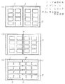
一般に製品として利用される回路形成基板は製造時のワークサイズより小さく、図2(a)に示すように、複数の集合回路形成基板12を一面に備えたワークサイズの状態から、金型打ち抜きやルータ加工等で切り出して個々の集合回路形成基板12を得る場合が多い。また、集合回路形成基板12も複数の個別回路形成基板13(後述)から構成されることが一般的である。
In general, a circuit forming substrate used as a product is smaller than a workpiece size at the time of manufacture. As shown in FIG. 2A, from a workpiece size state in which a plurality of collective
その際に、ワークサイズと集合回路形成基板のサイズ(以下製品サイズと記載)の整合性が製品コストに大きく影響する。 At that time, the consistency between the work size and the size of the collective circuit forming substrate (hereinafter referred to as product size) greatly affects the product cost.
すなわち、図2(a)の左右方向の大きさが500mmであったときに、製品サイズが100mmであれば、図2(a)に回路形成基板を上方より見た図を示すように、ツールマーク11等の有効でない部分を除いても左右方向に2枚の集合回路形成基板を並べて配置した際に効率良く設計が出来る。 That is, when the size in the left-right direction in FIG. 2A is 500 mm and the product size is 100 mm, as shown in FIG. Even when the ineffective portion such as the mark 11 is removed, the design can be efficiently performed when two collective circuit forming substrates are arranged side by side in the left-right direction.
しかしながら、製品サイズが150mmの場合や集合回路形成基板を少しでも多く配置したい場合には2枚のコア基板材料1をまたがる形で集合回路形成基板を配置せざるを得ない。 However, when the product size is 150 mm or when it is desired to arrange as many aggregate circuit formation substrates as possible, it is necessary to dispose the aggregate circuit formation substrate so as to straddle the two core substrate materials 1.
そのような配置を実現するために、あらかじめ2枚のコア形成基板材料1の当接する辺を制度良く切断しておき、2枚のコア形成基板材料1の間隔を極小にすることが有効である。 In order to realize such an arrangement, it is effective to systematically cut in advance the abutting sides of the two core-forming substrate materials 1 to minimize the distance between the two core-forming substrate materials 1. .
図2(b)に積層工程前にコア形成基板材料1を切断した例を示す。2枚のコア形成基板材料1が互いに当接する部位は、集合回路形成基板12を互いに隣接する部位とする。
FIG. 2B shows an example in which the core forming substrate material 1 is cut before the stacking process. The part where the two core-forming substrate materials 1 abut each other makes the collective
図2(c)に2枚のコア基板材料1をまたがる形で集合回路形成基板12aを配置した例を示す。
FIG. 2 (c) shows an example in which the collective
一般に集合回路形成基板12には携帯電話やデジタルスチルカメラのセットの一台分の個別回路形成基板を複数配置する場合が多い。セットを組み立てる際には集合回路形成基板12の状態で電子部品を実装し、その後に最終製品毎に個別回路形成基板に分割するのが実装効率の面から普通である。
In general, the collective
図3にその集合回路形成基板12aを上方より見た図を示す。
FIG. 3 shows a view of the collective
個別回路形成基板13の間に2枚のコア基板材料が当接する部位14が位置するように設計することが望ましい。
It is desirable to design so that the
コア基板材料当接部14は図3では直線状であるが製品状態回路形成基板の強度を増すために、図4に示すように2枚のコア形成基板材料1が噛み合う形状にすることも有効である。
The core substrate
発明者の検討では、切断方法にダイシング法を用い、2枚のコア回路形成基板材料1の間隔を100μmにすることも可能であった。 According to the inventor's study, it was possible to use a dicing method as a cutting method and to set the interval between the two core circuit forming substrate materials 1 to 100 μm.
切断方法には、ダイシング法の他にスリッタ刃を用いたり、レーザーによる切断法等の多くの方法が採用可能である。 As a cutting method, in addition to the dicing method, many methods such as a slitter blade or a laser cutting method can be employed.
本実施の形態では1枚のプリプレグ2に対して2枚のコア基板材料1を積層しているが、コア基板材料1の枚数を3枚以上の構成も採用可能であるし、2枚のプリプレグを並べて複数枚のコア基板材料1を積層する等の多様な組み合わせが採用できる。 In the present embodiment, two core substrate materials 1 are laminated on one prepreg 2, but it is possible to adopt a configuration in which the number of core substrate materials 1 is three or more, and two prepregs. Various combinations such as stacking a plurality of core substrate materials 1 side by side can be adopted.
また、プリプレグ2とコア基板材料1の組み合わせを厚み方向に多数段積層して高多層回路形成基板を製造することも可能である。 It is also possible to manufacture a high multilayer circuit forming substrate by stacking a number of combinations of the prepreg 2 and the core substrate material 1 in the thickness direction.
以上述べたように、本発明の構成によれば、回路形成基板の製造時のワークサイズを大きくした場合にも基板材料をハンドリングを安定させ、従来の製造方法に比較してより薄くサイズの大きな基板材料を用いて回路形成基板の製造が可能になり、その結果、導電性ペースト等の層間接続手段を用いた層間の電気的接続の信頼性をも大幅に向上させながら、高品質の高密度回路形成基板を提供することができ、産業上の利用可能性は大といえる。 As described above, according to the configuration of the present invention, even when the work size at the time of manufacturing a circuit-formed substrate is increased, the handling of the substrate material is stabilized, and it is thinner and larger in size than the conventional manufacturing method. It is possible to manufacture circuit-formed substrates using substrate materials, and as a result, high-quality and high-density while greatly improving the reliability of electrical connection between layers using interlayer connection means such as conductive paste A circuit forming substrate can be provided, and industrial applicability is great.
1 コア基板材料
2 プリプレグ
3 層間接続部
4 ビア穴
5 導電性ペースト
6 銅箔
7 回路
8 シート
9 レーザービア穴
10 レーザービア
11 ツールマーク
12、12a 集合回路形成基板
13 個別回路形成基板
14 コア基板材料当接部
DESCRIPTION OF SYMBOLS 1 Core substrate material 2 Prepreg 3 Interlayer connection part 4 Via hole 5 Conductive paste 6
Claims (6)
(2)層間接続手段を備えたBステージ状態基板材料
(3)回路、金属箔、層間接続手段のうち一つ以上を備えたBステージ状態基板材料
(4)回路もしくは金属箔を備えたCステージ状態基板材料もしくは回路もしくは金属箔と層間接続手段を備えたCステージ状態基板材料
のうち、
少なくとも1種以上の前記Bステージ状態基板材料及び2種以上の前記金属箔もしくは前記基板材料を積層物として積層し仮止めする積層工程と、
前記積層物の表層に回路を形成し多層の回路形成基板とする工程とを備え、
前記回路形成基板は複数の個別回路形成基板で構成される集合回路形成基板が複数配置されたものであり、
前記積層物を積層し仮止めする積層工程は、
1枚の前記Bステージ状態基板材料に対して2枚の前記Cステージ状態基板材料を互いに当接して積層し、
前記集合回路形成基板のいくつかは2枚の前記Cステージ状態基板材料をまたがる形で配置されることを特徴とする回路形成基板の製造方法。 (1) Metal foil, or metal foil attached to a support, or metal foil attached to a support and formed with a circuit pattern (2) B-stage state substrate material provided with interlayer connection means (3) Circuit, metal B stage state substrate material provided with one or more of foil and interlayer connection means (4) C stage state substrate material provided with circuit or metal foil or C stage state substrate material provided with circuit or metal foil and interlayer connection means Out of
A laminating step of laminating and temporarily fixing at least one kind of the B-stage state substrate material and two or more kinds of the metal foil or the substrate material as a laminate ;
Forming a circuit on the surface layer of the laminate to form a multilayer circuit forming substrate,
The circuit formation substrate is a plurality of collective circuit formation substrates arranged with a plurality of individual circuit formation substrates,
The laminating step of laminating and temporarily fixing the laminate is
Two sheets of the C-stage state substrate material are in contact with each other and laminated on one sheet of the B-stage state substrate material,
Some method of manufacturing circuit board, characterized in Rukoto arranged in the form across two of said C-stage state substrate material of the collective circuit forming board.
多層の回路形成基板の表層はレーザービアを備えることを特徴とする請求項3または請求項4に記載の回路形成基板の製造方法。 The C stage state substrate material has an interlayer connection formed of a circuit and a conductive paste on the surface,
5. The method of manufacturing a circuit forming substrate according to claim 3, wherein the surface layer of the multilayer circuit forming substrate includes a laser via.
Priority Applications (5)
| Application Number | Priority Date | Filing Date | Title |
|---|---|---|---|
| JP2005076815A JP4617941B2 (en) | 2005-03-17 | 2005-03-17 | Method for manufacturing circuit-formed substrate |
| US11/814,037 US7685707B2 (en) | 2005-03-17 | 2006-03-16 | Method for manufacturing circuit forming substrate |
| PCT/JP2006/305252 WO2006098406A1 (en) | 2005-03-17 | 2006-03-16 | Method for manufacturing circuit forming board |
| TW095108967A TW200640327A (en) | 2005-03-17 | 2006-03-16 | Method of manufacturing circuit forming board |
| CN2006800081638A CN101142863B (en) | 2005-03-17 | 2006-03-16 | Method for manufacturing circuit forming board |
Applications Claiming Priority (1)
| Application Number | Priority Date | Filing Date | Title |
|---|---|---|---|
| JP2005076815A JP4617941B2 (en) | 2005-03-17 | 2005-03-17 | Method for manufacturing circuit-formed substrate |
Publications (3)
| Publication Number | Publication Date |
|---|---|
| JP2006261390A JP2006261390A (en) | 2006-09-28 |
| JP2006261390A5 JP2006261390A5 (en) | 2008-05-01 |
| JP4617941B2 true JP4617941B2 (en) | 2011-01-26 |
Family
ID=36991747
Family Applications (1)
| Application Number | Title | Priority Date | Filing Date |
|---|---|---|---|
| JP2005076815A Expired - Fee Related JP4617941B2 (en) | 2005-03-17 | 2005-03-17 | Method for manufacturing circuit-formed substrate |
Country Status (5)
| Country | Link |
|---|---|
| US (1) | US7685707B2 (en) |
| JP (1) | JP4617941B2 (en) |
| CN (1) | CN101142863B (en) |
| TW (1) | TW200640327A (en) |
| WO (1) | WO2006098406A1 (en) |
Families Citing this family (8)
| Publication number | Priority date | Publication date | Assignee | Title |
|---|---|---|---|---|
| JP5061673B2 (en) * | 2007-03-19 | 2012-10-31 | パナソニック株式会社 | Circuit board and circuit board manufacturing method |
| JP5041291B2 (en) * | 2007-11-05 | 2012-10-03 | 大日本印刷株式会社 | Non-contact IC card manufacturing method |
| US20120090883A1 (en) * | 2010-10-13 | 2012-04-19 | Qualcomm Incorporated | Method and Apparatus for Improving Substrate Warpage |
| CN102595809A (en) * | 2012-03-14 | 2012-07-18 | 柏承科技(昆山)股份有限公司 | Method for manufacturing high-density interconnection printed circuit board |
| CN102625604B (en) * | 2012-03-20 | 2014-10-01 | 柏承科技(昆山)股份有限公司 | Manufacturing method for high-density interconnection printed board |
| CN103369872A (en) * | 2012-03-30 | 2013-10-23 | 北大方正集团有限公司 | Method for laminating multilayer printed circuit board |
| CN103338600A (en) * | 2013-05-10 | 2013-10-02 | 华为技术有限公司 | PCB structure and production method thereof, and embedded device PCB production method |
| US10433413B2 (en) * | 2014-08-15 | 2019-10-01 | Unimicron Technology Corp. | Manufacturing method of circuit structure embedded with heat-dissipation block |
Citations (7)
| Publication number | Priority date | Publication date | Assignee | Title |
|---|---|---|---|---|
| JPH04286188A (en) * | 1991-03-15 | 1992-10-12 | Matsushita Electric Works Ltd | Manufacture of multilayer interconnection board |
| JPH08116171A (en) * | 1994-10-18 | 1996-05-07 | Matsushita Electric Ind Co Ltd | Manufacture of printed wiring board and multiple-chamfered film for manufacturing to be used in the method |
| JP2000133912A (en) * | 1998-10-27 | 2000-05-12 | Matsushita Electric Works Ltd | Metallic foil with resin and manufacture thereof |
| JP2000151102A (en) * | 1998-11-16 | 2000-05-30 | Matsushita Electric Ind Co Ltd | Manufacture of multilayer circuit board |
| JP2000216518A (en) * | 1999-01-21 | 2000-08-04 | Ibiden Co Ltd | Manufacture of printed wiring board |
| JP2000307246A (en) * | 1999-04-26 | 2000-11-02 | Matsushita Electric Ind Co Ltd | Manufacture of circuit forming substrate and material thereof |
| JP2001024326A (en) * | 1999-07-08 | 2001-01-26 | Hitachi Chem Co Ltd | Manufacture of multilayered printed wiring board |
Family Cites Families (15)
| Publication number | Priority date | Publication date | Assignee | Title |
|---|---|---|---|---|
| US5A (en) * | 1836-08-10 | Thomas blancharjq | ||
| US4A (en) * | 1836-08-10 | Stock | ||
| US2003A (en) * | 1841-03-12 | Improvement in horizontal windivhlls | ||
| US2001A (en) * | 1841-03-12 | Sawmill | ||
| US2000A (en) * | 1841-03-12 | Improvement in the manufacture of starch | ||
| US6A (en) * | 1836-08-10 | Thomas blanghard | ||
| US3795047A (en) * | 1972-06-15 | 1974-03-05 | Ibm | Electrical interconnect structuring for laminate assemblies and fabricating methods therefor |
| US5502889A (en) * | 1988-06-10 | 1996-04-02 | Sheldahl, Inc. | Method for electrically and mechanically connecting at least two conductive layers |
| US5175047A (en) * | 1990-08-09 | 1992-12-29 | Teledyne Industries, Inc. | Rigid-flex printed circuit |
| JPH05251865A (en) | 1991-02-28 | 1993-09-28 | Toppan Printing Co Ltd | Manufacture of printed-circuit board |
| JP2601128B2 (en) | 1992-05-06 | 1997-04-16 | 松下電器産業株式会社 | Method of manufacturing circuit forming substrate and circuit forming substrate |
| US5527998A (en) * | 1993-10-22 | 1996-06-18 | Sheldahl, Inc. | Flexible multilayer printed circuit boards and methods of manufacture |
| JP2937933B2 (en) * | 1997-03-24 | 1999-08-23 | 富山日本電気株式会社 | Manufacturing method of multilayer printed wiring board |
| TWI242398B (en) * | 2000-06-14 | 2005-10-21 | Matsushita Electric Ind Co Ltd | Printed circuit board and method of manufacturing the same |
| JP2003249753A (en) | 2002-02-25 | 2003-09-05 | Matsushita Electric Works Ltd | Method for producing multilayer printed wiring board |
-
2005
- 2005-03-17 JP JP2005076815A patent/JP4617941B2/en not_active Expired - Fee Related
-
2006
- 2006-03-16 WO PCT/JP2006/305252 patent/WO2006098406A1/en active Application Filing
- 2006-03-16 CN CN2006800081638A patent/CN101142863B/en not_active Expired - Fee Related
- 2006-03-16 TW TW095108967A patent/TW200640327A/en not_active IP Right Cessation
- 2006-03-16 US US11/814,037 patent/US7685707B2/en not_active Expired - Fee Related
Patent Citations (7)
| Publication number | Priority date | Publication date | Assignee | Title |
|---|---|---|---|---|
| JPH04286188A (en) * | 1991-03-15 | 1992-10-12 | Matsushita Electric Works Ltd | Manufacture of multilayer interconnection board |
| JPH08116171A (en) * | 1994-10-18 | 1996-05-07 | Matsushita Electric Ind Co Ltd | Manufacture of printed wiring board and multiple-chamfered film for manufacturing to be used in the method |
| JP2000133912A (en) * | 1998-10-27 | 2000-05-12 | Matsushita Electric Works Ltd | Metallic foil with resin and manufacture thereof |
| JP2000151102A (en) * | 1998-11-16 | 2000-05-30 | Matsushita Electric Ind Co Ltd | Manufacture of multilayer circuit board |
| JP2000216518A (en) * | 1999-01-21 | 2000-08-04 | Ibiden Co Ltd | Manufacture of printed wiring board |
| JP2000307246A (en) * | 1999-04-26 | 2000-11-02 | Matsushita Electric Ind Co Ltd | Manufacture of circuit forming substrate and material thereof |
| JP2001024326A (en) * | 1999-07-08 | 2001-01-26 | Hitachi Chem Co Ltd | Manufacture of multilayered printed wiring board |
Also Published As
| Publication number | Publication date |
|---|---|
| TWI372010B (en) | 2012-09-01 |
| US20090183366A1 (en) | 2009-07-23 |
| TW200640327A (en) | 2006-11-16 |
| CN101142863B (en) | 2012-08-29 |
| WO2006098406A1 (en) | 2006-09-21 |
| JP2006261390A (en) | 2006-09-28 |
| US7685707B2 (en) | 2010-03-30 |
| CN101142863A (en) | 2008-03-12 |
Similar Documents
| Publication | Publication Date | Title |
|---|---|---|
| JP4617941B2 (en) | Method for manufacturing circuit-formed substrate | |
| US9999134B2 (en) | Self-decap cavity fabrication process and structure | |
| JP5080234B2 (en) | Wiring board and manufacturing method thereof | |
| US9179553B2 (en) | Method of manufacturing multilayer wiring board | |
| KR101103301B1 (en) | A build-up printed circuit board with odd-layer and Manufacturing method of the same | |
| WO2010113448A1 (en) | Manufacturing method for circuit board, and circuit board | |
| JP5464760B2 (en) | Multilayer circuit board manufacturing method | |
| KR100897668B1 (en) | Fabricating Method of Printed Circuit Board using the Carrier | |
| JP2006049660A (en) | Manufacturing method of printed wiring board | |
| JP5302920B2 (en) | Manufacturing method of multilayer wiring board | |
| US20140182899A1 (en) | Rigid-flexible printed circuit board and method for manufacturing same | |
| JP5057653B2 (en) | Flex-rigid wiring board and manufacturing method thereof | |
| JP2010206124A (en) | Method of manufacturing multilayer circuit board, and multilayer circuit board | |
| KR101136396B1 (en) | PCB within cavity and Fabricaring method of the same | |
| JP2010225973A (en) | Manufacturing method of multilayer circuit board | |
| KR101167422B1 (en) | Carrier member and method of manufacturing PCB using the same | |
| KR101055455B1 (en) | Carrier member for substrate manufacturing and method for manufacturing substrate using same | |
| JP2006196567A (en) | Method for manufacturing circuit formation substrate | |
| KR101154605B1 (en) | The printed circuit board and the method for manufacturing the same | |
| JP2011040648A (en) | Method of manufacturing circuit board, and the circuit board | |
| JP2009212417A (en) | Method of manufacturing multilayer wiring board | |
| JP2008258358A (en) | Rigid flexible board and manufacturing method thereof | |
| JP2008235640A (en) | Circuit board and circuit board manufacturing method | |
| WO2015125267A1 (en) | Printed wiring board and manufacturing method for printed wiring board | |
| KR20180025345A (en) | Rigid flexible circuit board manufacturing method |
Legal Events
| Date | Code | Title | Description |
|---|---|---|---|
| A521 | Written amendment |
Free format text: JAPANESE INTERMEDIATE CODE: A523 Effective date: 20080313 |
|
| A621 | Written request for application examination |
Free format text: JAPANESE INTERMEDIATE CODE: A621 Effective date: 20080313 |
|
| RD01 | Notification of change of attorney |
Free format text: JAPANESE INTERMEDIATE CODE: A7421 Effective date: 20080414 |
|
| RD01 | Notification of change of attorney |
Free format text: JAPANESE INTERMEDIATE CODE: A7421 Effective date: 20091126 |
|
| A131 | Notification of reasons for refusal |
Free format text: JAPANESE INTERMEDIATE CODE: A131 Effective date: 20100713 |
|
| A521 | Written amendment |
Free format text: JAPANESE INTERMEDIATE CODE: A523 Effective date: 20100831 |
|
| TRDD | Decision of grant or rejection written | ||
| A01 | Written decision to grant a patent or to grant a registration (utility model) |
Free format text: JAPANESE INTERMEDIATE CODE: A01 Effective date: 20100928 |
|
| A01 | Written decision to grant a patent or to grant a registration (utility model) |
Free format text: JAPANESE INTERMEDIATE CODE: A01 |
|
| A61 | First payment of annual fees (during grant procedure) |
Free format text: JAPANESE INTERMEDIATE CODE: A61 Effective date: 20101011 |
|
| FPAY | Renewal fee payment (event date is renewal date of database) |
Free format text: PAYMENT UNTIL: 20131105 Year of fee payment: 3 |
|
| FPAY | Renewal fee payment (event date is renewal date of database) |
Free format text: PAYMENT UNTIL: 20131105 Year of fee payment: 3 |
|
| LAPS | Cancellation because of no payment of annual fees |