EP1158523A1 - Adressgenerator zur Erzeugung von Adressen für eine On-Chip Trimmschaltung - Google Patents
Adressgenerator zur Erzeugung von Adressen für eine On-Chip Trimmschaltung Download PDFInfo
- Publication number
- EP1158523A1 EP1158523A1 EP01110246A EP01110246A EP1158523A1 EP 1158523 A1 EP1158523 A1 EP 1158523A1 EP 01110246 A EP01110246 A EP 01110246A EP 01110246 A EP01110246 A EP 01110246A EP 1158523 A1 EP1158523 A1 EP 1158523A1
- Authority
- EP
- European Patent Office
- Prior art keywords
- address generator
- input
- address
- generator according
- memory
- Prior art date
- Legal status (The legal status is an assumption and is not a legal conclusion. Google has not performed a legal analysis and makes no representation as to the accuracy of the status listed.)
- Granted
Links
Images

Classifications
-
- G—PHYSICS
- G11—INFORMATION STORAGE
- G11C—STATIC STORES
- G11C29/00—Checking stores for correct operation ; Subsequent repair; Testing stores during standby or offline operation
- G11C29/02—Detection or location of defective auxiliary circuits, e.g. defective refresh counters
-
- G—PHYSICS
- G11—INFORMATION STORAGE
- G11C—STATIC STORES
- G11C29/00—Checking stores for correct operation ; Subsequent repair; Testing stores during standby or offline operation
- G11C29/02—Detection or location of defective auxiliary circuits, e.g. defective refresh counters
- G11C29/021—Detection or location of defective auxiliary circuits, e.g. defective refresh counters in voltage or current generators
-
- G—PHYSICS
- G11—INFORMATION STORAGE
- G11C—STATIC STORES
- G11C29/00—Checking stores for correct operation ; Subsequent repair; Testing stores during standby or offline operation
- G11C29/02—Detection or location of defective auxiliary circuits, e.g. defective refresh counters
- G11C29/028—Detection or location of defective auxiliary circuits, e.g. defective refresh counters with adaption or trimming of parameters
-
- G—PHYSICS
- G11—INFORMATION STORAGE
- G11C—STATIC STORES
- G11C5/00—Details of stores covered by group G11C11/00
- G11C5/14—Power supply arrangements, e.g. power down, chip selection or deselection, layout of wirings or power grids, or multiple supply levels
- G11C5/147—Voltage reference generators, voltage or current regulators; Internally lowered supply levels; Compensation for voltage drops
-
- G—PHYSICS
- G11—INFORMATION STORAGE
- G11C—STATIC STORES
- G11C8/00—Arrangements for selecting an address in a digital store
- G11C8/04—Arrangements for selecting an address in a digital store using a sequential addressing device, e.g. shift register, counter
Definitions
- the invention relates to an address generator for generation of addresses for an on-chip trim circuit, which are used for Matching generated on a semiconductor chip Serves as reference voltages.
- one according to the invention Address generator a certain number of one each Memory latch existing levels. Every latch is there executed as an edge-controlled flip-flop, as in synchronous counters is used. On the supply of one Clock signal to a clock input and a control signal can the address generator either as a counter or as Shift registers are operated. The number of levels is at least equal to 1.
- the levels of the address generator each have one of the previous ones mentioned electric fuses.
- Each memory latch points MOS transistors on the electrical fuses adapt address information to be supplied to the CMOS level.
- the memory latches have a common one Initialization input and a loading input and are such set up that a signal applied to the charging input only for intact (or shot) fuses, the Latch information in the initialization value brings complementary value.
- the inventive one advantageously optimizes Address generator the required area on the semiconductor chip and reduces the number of control lines. In particular the number of output lines to an external Test facility lowered to 1. Furthermore, the address generator according to the invention by the optional proposed extensions in an optimal way different functional requirements adaptable.
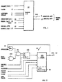
- Figure 1 shows a circuit block of a preferred one Embodiment of an inventive Address generator, generally designated 10 is designated.
- the address generator 10 in FIG. 1 is designed for M bits and thus contains M memory or register levels, each consist of a MOS memory latch (see FIG. 3).
- the address generator 10 With a "Counting" counting signal applied to an input 6 the address generator 10 is operated in the manner of a counter and counts 14 in for each clock signal at clock input Match with a count direction signal 16 up or backwards. With one at an input 5 Signal “push” is the address generator 10 as Shift registers can be operated.
- the Address generator contains electrical fuses and the am Loading input 11 parallel information individual bits of the address generator 10 only at each intact (or alternatively only with each shot) fuses in the complementary state to the initialization value brings.
- the electrical fuses can be polysilicon bridges, gate oxide bridges, Tungsten, aluminum, or other metal bridges his.
- the address generated by the address generator 10 lies a parallel output 8 with that mentioned Trim circuit is connected or connectable.
- the address generator 10 optionally has a test a serial input 12 and a serial output 13 with which the meter reading or the fuse information of the Address generator can be read out serially. It cannot destructive by feedback of the serial output 13 the serial input 12 by not shown in Fig. 1 Feedback links or destructive happen by others (Test) information is given to the serial input.
- the address generator 10 is also through a programming input 15 expandable, which in the memory latches of Address generator 10 available information bit by bit Programming of the corresponding fuses used.
- the address generator 10 can add an additional Memory latch 20 are expanded, in which the one Input 17 present signal of a (not shown) Voltage comparator (cf. DE 199 16 244.1) are adopted and can be output serially with the address value.
- a Voltage comparator cf. DE 199 16 244.1
- FIG. 2 shows a memory stage in the form of a block diagram 101 of the address generator 10 shown in FIG. 1. Here the serial and the parallel output coincide.
- Feedback elements 22, 23 serve to connect the output 13 feed back information to the serial input.
- the from the (serial) output 13 via the feedback elements 22 and 23 fed back information with the NAND gate 103 combined carry and serial input 12 are multiplexed by a multiplexer 102.
- FIG. 3 is a currently preferred implementation of a Memory latch stage 101 shown in FIG. 2.
- the memory latch stage 101 has MOS transistors 110, 111, 112 and 113 and an inverter 114.
- the charging input 11 is a via a MOS transistor 117 electric fuse 105 can be applied.
- FIG. 4 is a signal-time diagram for the test operation of the shown in Fig. 3 MOS latch circuit while FIG. 5 shows a truth table of the signal states of FIG. 3 MOS latch circuit shown depending on whether the electric fuse 105 is shot or not.
Landscapes
- Engineering & Computer Science (AREA)
- Power Engineering (AREA)
- Microelectronics & Electronic Packaging (AREA)
- Dram (AREA)
- For Increasing The Reliability Of Semiconductor Memories (AREA)
Abstract
Description
- Der Adressgenerator kann einen seriellen Eingang und einen seriellen Ausgang zum Auslesen des Zählerstands bzw. der Fuseinformation aufweisen;
- der Adressgenerator kann weiterhin Rückkopplungsglieder aufweisen, die den seriellen Ausgang wahlweise zum seriellen Eingang zurückkoppeln;
- Durch die Rückkopplung des seriellen Ausgangs auf den seriellen Eingang kann der Zählerstand bzw. die Fuseinformation nicht zerstörend am seriellen Ausgang ausgelesen werden. Andererseits kann andere, z.B. Testinformation an den seriellen Eingang angelegt und taktgesteuert in den Adressgenerator übernommen werden;
- es kann weiterhin ein Programmiereingang am Adressgenerator vorgesehen sein, um mit der in den Speicherlatches vorhandenen Information die Fuses bitweise zu programmieren;
- außerdem kann ein Vorwärts-Rückwärts-Wahleingang zur Wahl der Zählrichtung des Zählers bzw. der Schieberichtung des Schieberegisters des Adressgenerators vorgesehen sein;
- das Schieberegister des Adressgenerators kann um ein weiteres Speicherlatch (1 Bit) erweitert werden, in welches ein momentanes (JA/NEIN) Vergleichsergebnis eines Spannungskomparators speicherbar ist, der die momentane von der Trimmschaltung erzeugte Spannung mit einer externen Vergleichsspannung vergleicht. Das in dem zusätzlichen Speicherelement eingespeicherte Vergleichsergebnis kann dann zusammen mit dem generierten Adressenwert am seriellen Ausgang ausgegeben werden.
Claims (8)
- Adressgenerator zur Erzeugung von Adressen für eine On-Chip-Trimmschaltung zur Abstimmung einer auf einem Halbleiterchip erzeugten Referenzspannung,
dadurch gekennzeichnet, dass der Adressgenerator (10) eine bestimmte Anzahl M von aus jeweils einem Speicherlatch bestehenden Stufen (1, 2, 3, ..., M) aufweist, die auf ein einem Steuereingang (5,6) des Adressgenerators (10) zugeführtes Steuersignal und auf ein einem Takteingang (14) desselben angelegtes Taktsignal wahlweise als synchroner Zähler oder als Schieberegister betreibbar sind, wobei M gleich oder größer als 1 ist. - Adressgenerator nach Anspruch 1,
dadurch gekennzeichnet, dass der Adressgenerator (10) elektrische Fuses (105) aufweist, in denen eine vom Adressgenerator generierte Adresse für die Trimschaltung bei Übereinstimmung einer veränderlichen Referenzspannung des Chips mit einer von außen zugeführten Vergleichsspannung dauerhaft speicherbar ist, und dass die Speicherlatches des Adressgenerators MOS-Transistoren in einer zur Anpassung des Pegels der den elektrischen Fuses (105) zuzuführenden Adressinformation an den CMOS-Pegel eingerichteten Anordnung aufweist. - Adressgenerator nach Anspruch 1 oder 2,
dadurchgekennzeichnet, dass die Speicherlatches einen gemeinsamen Initialisierungseingang (7) und einen Ladeeingang (11) so aufweisen, dass ein am Ladeeingang angelegtes Signal nur bei jeweils intakter (oder geschossener) Fuse (105) die jeweilige Latchinformation des Speicherlatches in den zum Initialisierungswert komplementären Wert bringt. - Adressgenerator nach einem der vorangehenden Ansprüche,
dadurch gekennzeichnet, dass er weiterhin einen seriellen Eingang (12) und einen seriellen Ausgang (13) aufweist, um den Zählerstand bzw. die Fuseinformation seriell auszulesen. - Adressgenerator nach Anspruch 4,
dadurch gekennzeichnet, dass er weiterhin Rückkopplungsglieder (22,23) aufweist, die den seriellen Ausgang (13) wahlweise zum seriellen Eingang (12) zurückkoppeln. - Adressgenerator nach einem der vorangehenden Ansprüche,
dadurch gekennzeichnet, dass er weiterhin einen Programmiereingang (15) aufweist, um mit der in den Speicherlatches vorhandenen Information bitweise die jeweiligen Fuses zu programmieren. - Adressgenerator nach einem der vorangehenden Ansprüche,
dadurch gekennzeichnet, dass weiterhin ein Zählrichtungswähleingang (16) vorgesehen ist. - Adressgenerator nach einem der vorangehenden Ansprüche,
dadurch gekennzeichnet, dass er weiterhin ein zusätzliches Speicherlatch (20) aufweist, in welches ein momentanes (JA/NEIN) Vergleichsergebnis eines Spannungskomparators, der die momentan von der Trimmschaltung erzeugte Spannung mit der externen Vergleichsspannung vergleicht, speicherbar und zusammen mit den generierten Adresswerten am seriellen Ausgang ausgebbar ist.
Applications Claiming Priority (2)
| Application Number | Priority Date | Filing Date | Title |
|---|---|---|---|
| DE10022767A DE10022767C2 (de) | 2000-05-10 | 2000-05-10 | Adressgenerator zur Erzeugung von Adressen für eine On-Chip Trimmschaltung |
| DE10022767 | 2000-05-10 |
Publications (2)
| Publication Number | Publication Date |
|---|---|
| EP1158523A1 true EP1158523A1 (de) | 2001-11-28 |
| EP1158523B1 EP1158523B1 (de) | 2008-02-27 |
Family
ID=7641446
Family Applications (1)
| Application Number | Title | Priority Date | Filing Date |
|---|---|---|---|
| EP01110246A Expired - Lifetime EP1158523B1 (de) | 2000-05-10 | 2001-04-25 | Adressgenerator zur Erzeugung von Adressen für eine On-Chip Trimmschaltung |
Country Status (4)
| Country | Link |
|---|---|
| US (1) | US6459649B2 (de) |
| EP (1) | EP1158523B1 (de) |
| DE (2) | DE10022767C2 (de) |
| TW (1) | TW516210B (de) |
Families Citing this family (8)
| Publication number | Priority date | Publication date | Assignee | Title |
|---|---|---|---|---|
| JP2001176975A (ja) * | 1999-12-17 | 2001-06-29 | Mitsubishi Electric Corp | 半導体装置及びその製造方法 |
| JP4278325B2 (ja) | 2001-12-19 | 2009-06-10 | 株式会社ルネサステクノロジ | 半導体集積回路装置 |
| DE10238279B4 (de) * | 2002-08-21 | 2005-05-25 | Infineon Technologies Ag | Schieberegisterkette zur Trimmung von Generatoren einer integrierten Halbleitervorrichtung |
| US6738298B1 (en) | 2002-11-18 | 2004-05-18 | Micron Technology, Inc. | Automatic reference voltage regulation in a memory device |
| US20040120482A1 (en) * | 2002-12-20 | 2004-06-24 | Bentley Ronald Locker | System and method for reducing disruption in a DSL environment caused by a pots transient event |
| US7219829B2 (en) * | 2002-12-24 | 2007-05-22 | Tracey Treat | Carrier which is aesthetically irreversibly convertible from planar blank to closed package for coded card and methods for manufacture and use of the same |
| US7248102B2 (en) * | 2005-01-20 | 2007-07-24 | Infineon Technologies Ag | Internal reference voltage generation for integrated circuit testing |
| CN109450433B (zh) * | 2018-08-02 | 2022-08-05 | 上海芯哲微电子科技股份有限公司 | 一种双路集成电路修调装置 |
Citations (4)
| Publication number | Priority date | Publication date | Assignee | Title |
|---|---|---|---|---|
| US3906195A (en) * | 1973-02-09 | 1975-09-16 | Takeda Riken Ind Co Ltd | Synchronous multi-purpose counter |
| US3978413A (en) * | 1975-02-07 | 1976-08-31 | Hewlett-Packard Company | Modulus counter circuit utilizing serial access |
| US5404049A (en) * | 1993-11-02 | 1995-04-04 | International Business Machines Corporation | Fuse blow circuit |
| US5982163A (en) * | 1997-04-11 | 1999-11-09 | Fujitsu Limited | Internal power source voltage trimming circuit |
Family Cites Families (5)
| Publication number | Priority date | Publication date | Assignee | Title |
|---|---|---|---|---|
| US5892719A (en) * | 1996-12-27 | 1999-04-06 | Kabushiki Kaisha Toshiba | Redundancy circuit technique applied DRAM of multi-bit I/O having overlaid-DQ bus |
| US5886940A (en) * | 1997-08-21 | 1999-03-23 | Micron Technology, Inc. | Self-protected circuit for non-selected programmable elements during programming |
| US5933370A (en) * | 1998-01-09 | 1999-08-03 | Information Storage Devices, Inc. | Trimbit circuit for flash memory |
| US5889727A (en) * | 1998-05-11 | 1999-03-30 | Texas Instruments--Acer Incorporated | Circuit for reducing the transmission delay of the redundancy evaluation for synchronous DRAM |
| DE19960244C1 (de) * | 1999-12-14 | 2001-02-01 | Infineon Technologies Ag | Anordnung zum Trimmen von Referenzspannungen in Halbleiterchips, insb. Halbleiterspeichern |
-
2000
- 2000-05-10 DE DE10022767A patent/DE10022767C2/de not_active Expired - Fee Related
-
2001
- 2001-04-25 DE DE50113649T patent/DE50113649D1/de not_active Expired - Fee Related
- 2001-04-25 EP EP01110246A patent/EP1158523B1/de not_active Expired - Lifetime
- 2001-05-09 TW TW090111042A patent/TW516210B/zh not_active IP Right Cessation
- 2001-05-10 US US09/854,258 patent/US6459649B2/en not_active Expired - Fee Related
Patent Citations (4)
| Publication number | Priority date | Publication date | Assignee | Title |
|---|---|---|---|---|
| US3906195A (en) * | 1973-02-09 | 1975-09-16 | Takeda Riken Ind Co Ltd | Synchronous multi-purpose counter |
| US3978413A (en) * | 1975-02-07 | 1976-08-31 | Hewlett-Packard Company | Modulus counter circuit utilizing serial access |
| US5404049A (en) * | 1993-11-02 | 1995-04-04 | International Business Machines Corporation | Fuse blow circuit |
| US5982163A (en) * | 1997-04-11 | 1999-11-09 | Fujitsu Limited | Internal power source voltage trimming circuit |
Also Published As
| Publication number | Publication date |
|---|---|
| DE10022767A1 (de) | 2001-11-22 |
| US6459649B2 (en) | 2002-10-01 |
| DE50113649D1 (de) | 2008-04-10 |
| EP1158523B1 (de) | 2008-02-27 |
| DE10022767C2 (de) | 2002-03-28 |
| TW516210B (en) | 2003-01-01 |
| US20010054127A1 (en) | 2001-12-20 |
Similar Documents
| Publication | Publication Date | Title |
|---|---|---|
| DE4041897C2 (de) | Integrierte Schaltkreiseinrichtung und Abtastpfadsystem | |
| DE3884037T2 (de) | Programmierungsschaltung für Eingabe-/Ausgabezelle eines programmierbaren Logikarrays. | |
| DE68921088T2 (de) | Integrierte Halbleiterschaltung. | |
| DE3788586T2 (de) | Schaltung zur Prüfung des Eingangsspannungssignals für eine halbleiterintegrierte Schaltung. | |
| DE10056592A1 (de) | Anordnung mit einem Mikroprozessor | |
| DE69717893T2 (de) | Ausgangpufferschaltung | |
| DE3871889T2 (de) | Programmierbare eingangs-/ausgangsschaltung. | |
| DE3750704T2 (de) | Datenprozessor. | |
| DE2750344C2 (de) | Logikschaltung zum Betätigen irgendeiner Teilmenge einer Mehrzahl von Vorrichtungen | |
| WO2000070761A1 (de) | Schaltungsanordnung zur erzeugung von strompulsen im versorgungsstrom integrierter schaltungen | |
| DE10022767C2 (de) | Adressgenerator zur Erzeugung von Adressen für eine On-Chip Trimmschaltung | |
| DE4018296A1 (de) | Elektrische schaltung fuer einen parallelschreibtest eines breiten mehrfachbytes in einer halbleiterspeichereinrichtung | |
| DE3689879T2 (de) | Arithmetisch-logische Schaltung. | |
| DE102006030888B4 (de) | Verfahren und Vorrichtung zum Erzeugen eines Startwertes für einen Pseudo-Zufallszahlengenerator | |
| DE4416171A1 (de) | EEPROM-Vorrichtung | |
| DE69608303T2 (de) | Anordnung und verfahren zur programmierung von hochimpedanzzuständen auf bestimmte ein-/ausgangsanschlussflächen | |
| DE112018005329T5 (de) | Analog-digital-wandlungsvorrichtung | |
| DE3780551T2 (de) | Speichereinrichtung unter verwendung von adressenmultiplex. | |
| DE19603087C2 (de) | Vorrichtung und Verfahren zur Steuerung eines Taktsignals in einer Halbleiterschaltung | |
| DE69523537T2 (de) | Analog-Digital-Wandler mit schreibbarem Ergebnisregister | |
| DE69618344T2 (de) | Schaltung um redundante Daten einer Redundanzschaltung innerhalb einer Speicheranordnung durch zeitgeteilte Annäherung zu übertragen | |
| DE69524529T2 (de) | Halbleiterspeicheranordnung und Verfahren zur Herstellung | |
| DE69121804T2 (de) | Halbleiterspeicheranordnung | |
| DE10102349C1 (de) | Verfahren und Schaltungsanordnung zur Kennzeichnung einer Betriebseigenschaft einer integrierten Schaltung | |
| EP0404985B1 (de) | Schaltungsanordnung zur Identifikation integrierter Halbleiterschaltkreise |
Legal Events
| Date | Code | Title | Description |
|---|---|---|---|
| PUAI | Public reference made under article 153(3) epc to a published international application that has entered the european phase |
Free format text: ORIGINAL CODE: 0009012 |
|
| AK | Designated contracting states |
Kind code of ref document: A1 Designated state(s): AT BE CH CY DE DK ES FI FR GB GR IE IT LI LU MC NL PT SE TR Kind code of ref document: A1 Designated state(s): DE FR GB IE IT |
|
| AX | Request for extension of the european patent |
Free format text: AL;LT;LV;MK;RO;SI |
|
| 17P | Request for examination filed |
Effective date: 20011218 |
|
| AKX | Designation fees paid |
Free format text: DE FR GB IE IT |
|
| 17Q | First examination report despatched |
Effective date: 20060627 |
|
| GRAP | Despatch of communication of intention to grant a patent |
Free format text: ORIGINAL CODE: EPIDOSNIGR1 |
|
| GRAS | Grant fee paid |
Free format text: ORIGINAL CODE: EPIDOSNIGR3 |
|
| GRAA | (expected) grant |
Free format text: ORIGINAL CODE: 0009210 |
|
| AK | Designated contracting states |
Kind code of ref document: B1 Designated state(s): DE FR GB IE IT |
|
| REG | Reference to a national code |
Ref country code: GB Ref legal event code: FG4D Free format text: NOT ENGLISH |
|
| REG | Reference to a national code |
Ref country code: IE Ref legal event code: FG4D Free format text: LANGUAGE OF EP DOCUMENT: GERMAN |
|
| REF | Corresponds to: |
Ref document number: 50113649 Country of ref document: DE Date of ref document: 20080410 Kind code of ref document: P |
|
| PGFP | Annual fee paid to national office [announced via postgrant information from national office to epo] |
Ref country code: DE Payment date: 20080613 Year of fee payment: 8 |
|
| REG | Reference to a national code |
Ref country code: IE Ref legal event code: FD4D |
|
| PG25 | Lapsed in a contracting state [announced via postgrant information from national office to epo] |
Ref country code: IE Free format text: LAPSE BECAUSE OF FAILURE TO SUBMIT A TRANSLATION OF THE DESCRIPTION OR TO PAY THE FEE WITHIN THE PRESCRIBED TIME-LIMIT Effective date: 20080227 |
|
| EN | Fr: translation not filed | ||
| PLBE | No opposition filed within time limit |
Free format text: ORIGINAL CODE: 0009261 |
|
| STAA | Information on the status of an ep patent application or granted ep patent |
Free format text: STATUS: NO OPPOSITION FILED WITHIN TIME LIMIT |
|
| GBPC | Gb: european patent ceased through non-payment of renewal fee |
Effective date: 20080527 |
|
| 26N | No opposition filed |
Effective date: 20081128 |
|
| PG25 | Lapsed in a contracting state [announced via postgrant information from national office to epo] |
Ref country code: FR Free format text: LAPSE BECAUSE OF FAILURE TO SUBMIT A TRANSLATION OF THE DESCRIPTION OR TO PAY THE FEE WITHIN THE PRESCRIBED TIME-LIMIT Effective date: 20081212 |
|
| PG25 | Lapsed in a contracting state [announced via postgrant information from national office to epo] |
Ref country code: GB Free format text: LAPSE BECAUSE OF NON-PAYMENT OF DUE FEES Effective date: 20080527 |
|
| PG25 | Lapsed in a contracting state [announced via postgrant information from national office to epo] |
Ref country code: IT Free format text: LAPSE BECAUSE OF FAILURE TO SUBMIT A TRANSLATION OF THE DESCRIPTION OR TO PAY THE FEE WITHIN THE PRESCRIBED TIME-LIMIT Effective date: 20080227 |
|
| PG25 | Lapsed in a contracting state [announced via postgrant information from national office to epo] |
Ref country code: DE Free format text: LAPSE BECAUSE OF NON-PAYMENT OF DUE FEES Effective date: 20091103 |