EP1157143B1 - Mt cvd process - Google Patents
Mt cvd process Download PDFInfo
- Publication number
- EP1157143B1 EP1157143B1 EP00913591A EP00913591A EP1157143B1 EP 1157143 B1 EP1157143 B1 EP 1157143B1 EP 00913591 A EP00913591 A EP 00913591A EP 00913591 A EP00913591 A EP 00913591A EP 1157143 B1 EP1157143 B1 EP 1157143B1
- Authority
- EP
- European Patent Office
- Prior art keywords
- process described
- substrate
- group
- cermets
- ceramics
- Prior art date
- Legal status (The legal status is an assumption and is not a legal conclusion. Google has not performed a legal analysis and makes no representation as to the accuracy of the status listed.)
- Revoked
Links
Images

Classifications
-
- C—CHEMISTRY; METALLURGY
- C23—COATING METALLIC MATERIAL; COATING MATERIAL WITH METALLIC MATERIAL; CHEMICAL SURFACE TREATMENT; DIFFUSION TREATMENT OF METALLIC MATERIAL; COATING BY VACUUM EVAPORATION, BY SPUTTERING, BY ION IMPLANTATION OR BY CHEMICAL VAPOUR DEPOSITION, IN GENERAL; INHIBITING CORROSION OF METALLIC MATERIAL OR INCRUSTATION IN GENERAL
- C23C—COATING METALLIC MATERIAL; COATING MATERIAL WITH METALLIC MATERIAL; SURFACE TREATMENT OF METALLIC MATERIAL BY DIFFUSION INTO THE SURFACE, BY CHEMICAL CONVERSION OR SUBSTITUTION; COATING BY VACUUM EVAPORATION, BY SPUTTERING, BY ION IMPLANTATION OR BY CHEMICAL VAPOUR DEPOSITION, IN GENERAL
- C23C16/00—Chemical coating by decomposition of gaseous compounds, without leaving reaction products of surface material in the coating, i.e. chemical vapour deposition [CVD] processes
- C23C16/22—Chemical coating by decomposition of gaseous compounds, without leaving reaction products of surface material in the coating, i.e. chemical vapour deposition [CVD] processes characterised by the deposition of inorganic material, other than metallic material
- C23C16/30—Deposition of compounds, mixtures or solid solutions, e.g. borides, carbides, nitrides
- C23C16/36—Carbonitrides
-
- C—CHEMISTRY; METALLURGY
- C23—COATING METALLIC MATERIAL; COATING MATERIAL WITH METALLIC MATERIAL; CHEMICAL SURFACE TREATMENT; DIFFUSION TREATMENT OF METALLIC MATERIAL; COATING BY VACUUM EVAPORATION, BY SPUTTERING, BY ION IMPLANTATION OR BY CHEMICAL VAPOUR DEPOSITION, IN GENERAL; INHIBITING CORROSION OF METALLIC MATERIAL OR INCRUSTATION IN GENERAL
- C23C—COATING METALLIC MATERIAL; COATING MATERIAL WITH METALLIC MATERIAL; SURFACE TREATMENT OF METALLIC MATERIAL BY DIFFUSION INTO THE SURFACE, BY CHEMICAL CONVERSION OR SUBSTITUTION; COATING BY VACUUM EVAPORATION, BY SPUTTERING, BY ION IMPLANTATION OR BY CHEMICAL VAPOUR DEPOSITION, IN GENERAL
- C23C16/00—Chemical coating by decomposition of gaseous compounds, without leaving reaction products of surface material in the coating, i.e. chemical vapour deposition [CVD] processes
- C23C16/44—Chemical coating by decomposition of gaseous compounds, without leaving reaction products of surface material in the coating, i.e. chemical vapour deposition [CVD] processes characterised by the method of coating
-
- Y—GENERAL TAGGING OF NEW TECHNOLOGICAL DEVELOPMENTS; GENERAL TAGGING OF CROSS-SECTIONAL TECHNOLOGIES SPANNING OVER SEVERAL SECTIONS OF THE IPC; TECHNICAL SUBJECTS COVERED BY FORMER USPC CROSS-REFERENCE ART COLLECTIONS [XRACs] AND DIGESTS
- Y10—TECHNICAL SUBJECTS COVERED BY FORMER USPC
- Y10T—TECHNICAL SUBJECTS COVERED BY FORMER US CLASSIFICATION
- Y10T407/00—Cutters, for shaping
- Y10T407/27—Cutters, for shaping comprising tool of specific chemical composition
Definitions
- the present invention relates to a method for coating substrates using a MT (medium temperature) CVD process.
- Chemical vapor deposition is used to apply single or multiple layers of coatings to substrate surfaces.
- the thickness of each coating layer may be on the order of a fraction of a micron to around twenty microns.
- a gas or gases containing the atoms that will make up the coating are reduced or decomposed on or very near to a substrate surface at high temperatures so that a coating of a desired composition is deposited onto the substrate.
- the deposition can be a metal, a semiconductor, an alloy or a refractory compound.
- MT CVD differs from CVD in that the reaction temperatures used for MT CVD are significantly lower than those used for CVD. Often the temperature difference is on the order of hundreds of degrees.
- One way of achieving the reduced temperature of MT CVD is by the use of a reactant gas or gases that are capable of reacting to form the desired coating at the lower temperatures.
- TiCN coatings can be deposited by either CVD or MT CVD.
- the deposition of a TiCN coating by CVD and by MT CVD has been found to be useful for imparting a wear resistant, hard coating on substrates.
- An example of a CVD process for depositing TiCN coatings is one which uses a deposition process gas containing methane (CH 4 ) as a reactant along with titanium tetrachloride (TiCl 4 ) and molecular hydrogen (H 2 ) to form a TiCN coating at a reaction temperature of about 1000°C. If the reactant gas CH 4 in this deposition process gas is replaced by CH 3 CN gas, a MT CVD process is obtained by which a TiCN coating can be deposited on a substrate in the reaction temperature range of 700 to 900°C.
- CH 4 methane
- TiCl 4 titanium tetrachloride
- H 2 molecular hydrogen
- a layer of TiCN is formed by a reaction that is represented by the following formula: TiCl 4 + CH 3 CN + 5/2 H 2 ⁇ TiCN + 4HCl + CH 4 .
- the inventor of the present invention has made the surprising discovery that the addition of, volumetrically, from about 1 to about 30% of HCl gas to a MT CVD deposition process gas which also comprises predetermined amounts of CH 3 CN, TiCl 4 , H 2 gases, and optionally N 2 gas, results in a significant increase in the deposition rate of the TiCN coating at a given reaction temperature.
- the present invention provides a method for coating at least one substrate with a coating of TiCN by a MT CVD process which includes heating a substrate or substrates to a reaction temperature in a reaction chamber and then introducing into the reaction chamber a deposition process gas comprising from about 1 to about 30% HCl and predetermined amounts of CH 3 CN, TiCl 4 , H 2 , and optionally N 2 , so that a layer of TiCN deposits on the surface of the substrate or substrates.
- the present invention may be used with any desired substrate that is compatible with the MT CVD process.
- substrates include, but are not limited to ceramics, cemented carbides, cermets, high speed steels and other types of steels.
- the present invention may be used with substrates on which one or more coating layers of TiCN or of other coating compositions have been applied.
- the present invention may also be used to deposit a layer or layers of TiCN which will subsequently, or even intermittently, be overlaid with coating layers deposited by other methods. These underlying or overlaying layers may be applied by the method of the present invention or by other coating deposition methods. Examples of such other coating deposition methods include, but are not limited to, CVD, conventional MT CVD, physical vapor deposition (PVD), or combinations and variations thereof including those variations which use plasma enhancements.
- PVD physical vapor deposition
- a reference herein to applying a coating of TiCN by a method of the present invention to the surface of a substrate where, at the moment prior to applying the TiCN layer, the substrate already has three preexisting coating layers with a layer of TiN as the innermost layer, a layer of TiCN as an intermediate layer, and another layer of TiN as an outermost layer that reference is to be understood as referring to applying a TiCN coating by a method of the present invention to the outside surface of the outermost layer of TiN.
- the substrate that is to be coated by the present invention may be of any geometry compatible with the MT CVD process.
- the present invention is particularly useful for coating cutting tools of various geometries.
- the present invention may be used with, but is not limited to use with, substrates in the form of cutting tools for turning, milling or hole making.
- cutting tools include, but are not limited to, indexable cutting inserts and elongate rotary tools such as drills, end mills, taps, reamers, and broaches.
- the inventor has also discovered the surprising result that in some embodiments of the present invention, the significant increase in deposition rate of the TiCN coating is accompanied by a significant improvement in the uniformity of the deposited TiCN coating thicknesses throughout the MT CVD reaction chamber.
- This aspect of the present invention is particularly advantageous when a plurality of substrates located throughout a reaction chamber are being simultaneously coated.
- the prior art MT CVD processes that employ CH 3 CN cause a variability in the thickness of the TiCN coating deposited on the substrates depending on the location of a particular substrate with respect to the location of the entry into the reaction chamber of the deposition process gas.
- Some preferred embodiments of the present invention significantly reduce this location-dependent TiCN coating thickness variability while at the same time increasing the deposition rate of the TiCN coating.
- the inventor has also discovered the surprising result that the TiCN coating deposition rate and the uniformity of the TiCN coating thickness applied during the MT CVD process can be further controlled by the use of a temperature gradient in the reaction chamber in conjunction with the use of a deposition process gas comprising from about 1 to about 30% HCl and predetermined amounts of CH 3 CN, TiCl 4 , H 2 , and optionally N 2 .
- the present invention also includes embodiments for coating at least one substrate with a coating of TiCN by a MT CVD process which includes maintaining a temperature gradient in the reaction chamber during the introduction into the reaction chamber of a deposition process gas comprising from about 1 to about 30% HCl and predetermined amounts of CH 3 CN, TiCl 4 , H 2 , and optionally N 2 , so that a layer of TiCN is deposited on the surface of the substrate or substrates.
- the inventor also contemplates the present invention to include the use of a deposition process gas wherein one or more of the aforementioned component gases are replaced in whole or in part by another gas or gases.
- a deposition process gas wherein one or more of the aforementioned component gases are replaced in whole or in part by another gas or gases.
- CH 3 CN may be replaced by another gaseous compound which can act as a carbon/nitrogen source for the deposited coating
- HCl may be replaced by another gaseous hydrogen halide
- TiCl 4 may be replaced by another gaseous metal-halogen compound as a metal source for the coating.
- the inventor also contemplates the present invention to include the use of a deposition process gas wherein predetermined amounts of one or more additional reactive gases are included in the deposition process gas.
- the inventor contemplates in some embodiments that predetermined amounts of one or more additional reactive gases may be added that supply one or more additional elements to the coating, such as oxygen or boron.
- additional reactive gases may be added that supply one or more additional elements to the coating, such as oxygen or boron.
- Embodiments of the present invention which include such deposition process gas replacements and additions may result in the deposition of a carbonitride-containing coating other than TiCN.
- Such other carbonitride-containing coatings include oxycarbonitride and borocarbonitride coatings.
- the present invention comprises a method for coating at least one substrate with a carbonitride-containing coating by a MT CVD process which includes heating a substrate or substrates to a reaction temperature in a reaction chamber and then introducing into the reaction chamber a deposition process gas comprising from about 1 to about 30% of a hydrogen halide and predetermined amounts of a carbon/nitrogen source, a metal-halogen compound, H 2 , and optionally N 2 so that a layer of the carbonitride-containing coating deposits on the surface of the substrates or substrates.
- the deposition process gas may also include predetermined amounts of an additional reactive gas or gases.
- the present invention also comprises a method for coating at least one substrate with a carbonitride-containing coating by a MT CVD process which includes maintaining a temperature gradient in the reaction chamber during the introduction into the reaction chamber of a deposition process gas comprising from about 1 to about 30% of a hydrogen halide and predetermined amounts of a carbon/nitrogen source, a metal-halogen compound, H 2 , and optionally N 2 so that a layer of the carbonitride-containing coating is deposited on the surface of the substrate or substrates.
- the deposition process gas may also include predetermined amounts of an additional reactive gas or gases.
- FIG 1. shows a schematic of a cross-section of a conventional MT CVD reaction vessel.
- FIG 2. shows a schematic of an enlarged cross-section of a portion of a substrate coated in Test A.
- the MT CVD process is conducted using the following deposition process gas composition, reaction temperature, and reaction chamber pressure ranges.
- the deposition process gas preferably contains, volumetrically, from about 1 to about 30% HCl from about 0.2 to about 3.0% CH 3 CN, from about 0.5 to about 5.0% TiCl 4 , from 0 to about 35% N 2 , and from about 40 to about 98% H 2 . More preferably the deposition process gas contains from about 2.3 to about 20% HCl, from about 0.3 to about 0.7% CH 3 CN, from about 0.9 to about 2.1% TiCl 4 , from about 10 to about 30% N 2 , and from about 50 to about 85% H 2 .
- the reaction temperature is preferably in the range of from about 550 to about 900°C and more preferably from about 700 to less than about 900°C. Most preferably, the reaction temperature is in the range of from about 830 to about 880°C.
- a temperature gradient is used in the reaction chamber so that the substrate or substrates proximal to the entrance location or locations of the deposition process gas are heated to a lower reaction temperature than the substrate or substrates most remote from the entrance location or locations of the deposition process gas.
- the inventor has found that such a gradient can be used to further control the TiCN coating deposition rate and the uniformity of the TiCN coating thickness applied during the MT CVD process conducted in accordance with the present invention.
- such a temperature gradient is in the range of about from 10 to about 100°C and more preferably in the range of about 30 to about 50°C.
- the reaction pressure is preferably in the range of from about 5 to about 800 Torr (about 0.7 to about 107 kN m -2 ). More preferably, the reaction pressure is in the range of about 40 to about 120 Torr (about 5 to about 16 kN m -2 ).
- a deposition process gas is used wherein one or more of the component gases of HCl, CH 3 CN, and TiCl 4 are substituted in whole or in part by another gas.
- a deposition process gas is used in which the component gas CH 3 CN is replaced, in whole or in part, by another carbon-nitrogen source for the coating such as one or more of the gases monomethylamine (CH 3 NH 2 ), dimethylamine ((CH 3 ) 2 NH), trimethylamine ((CH 3 ) 3 N), hydrogen cyanide (HCN), and dimethylhydrazine (CH 3 (NH) 2 CH 3 ).
- some embodiments of the present invention include the use of a deposition process gas wherein HCl is replaced, in whole or in part, by another hydrogen halide such as hydrogen iodide (HI), hydrogen bromide (HBr) or hydrogen flouride (HF).
- a deposition process gas wherein TiCl 4 is replaced, in whole or in part, by another gas or gases which act as a Ti metal source for the coating, such as the flourides, bromides, or iodides of Ti.
- a deposition process gas is used in which predetermined amounts of one or more additional reactive gases are included.
- the deposition process gas may include predetermined amounts at least one of carbon monoxide (CO) and carbon dioxide (CO 2 ).
- the deposited coating may be a carbonitride-containing coating other than TiCN.
- the coating which is deposited may contain the metal of that chloride, flouride, bromide or iodide substituting in whole or in part for Ti thus producing a coating of a carbonitride of Hf, Nb, V, Zr, or Ta or their alloys or mixtures with each other and/or titanium.
- zirconium tetrachloride (ZrCl 4 ) is wholly substituted for TiCl 4 in the deposition process gas, a coating of ZrCN is deposited instead of TiCN.
- embodiments of the present invention employing an additional gas component or components in the deposition process gas may result in carbonitride-containing coatings other than TiCN being deposited.
- the addition of carbon monoxide (CO) or carbon dioxide (CO 2 ) to the deposition process gas may result in the deposition of the carbonitride-containing coating titanium oxycarbonitride (TiCON).
- the process deposition gas includes both an addition of CO or CO 2 and a substitution for TiCl 4 with a chloride, flouride, bromide or iodide of Hf, Nb, V, Zr, or Ta or their mixtures and alloys with each other and/or titanium
- a carbonitride-containing coating of an oxycarbonitride of Hf, Nb, V, Zr, or Ta or their alloys or mixtures with each other and/or titanium is deposited.
- the addition of boron chloride (BCl 3 ) to the deposition process gas results in the deposition of the carbonitride-containing coating titanium borocarbonitride (TiBCN).
- the process deposition gas includes both an addition of BCl 3 and a substitution for TiCl 4 with a chloride, flouride, bromide or iodide of Hf, Nb, V, Zr, or Ta or their alloys or mixtures with each other and/or titanium
- a carbonitride-containing coating of a borocarbonitride of Hf, Nb, V, Zr, or Ta or their alloys or mixtures with each other and/or titanium is deposited.
- the MT CVD reaction pressure is in the range of from about 5 to about 800 Torr (about 0.7 to about 107 kN m -2 )
- the reaction temperature is in the range of from about 550 to about 900°C, and, where a temperature gradient is used, the temperature gradient is in the range of from about 10 to about 100°C.
- the deposition process gas preferably contains, volumetrically, from about 1 to about 30% of a hydrogen halide, from about 0.2 to about 3.0% of a carbon/nitrogen source, from about 0.5 to about 5.0% of a metal-halogen compound, from 0 to about 35% N 2 , and from about 40 to about 98% H 2 .
- the deposition process gas also includes predetermined amounts of one or more additional reactive gases, such as CO or CO 2 , the amount of each such additional gas is preferably from about 0.1 to about 5.0%.
- Tests were conducted to compare the TiCN coating deposition rate and coating thickness uniformity throughout the reaction chamber produced by an embodiment of the present invention with that produced by a conventional MT CVD technique. Similar processing conditions were used for both tests.
- the tests consisted of applying a single coating of TiCN on a substrate. The TiCN coating thickness was then measured using a standard measurement technique on samples taken from predetermined locations throughout the reaction chamber. These locations were at varying distances from the entrance of the deposition process gas into the reaction chamber.
- the MT CVD process tests were conducted in a conventional MT CVD reaction vessel having a retort with a diameter of approximately 20 inches (51 cm) and a length approximately 43.5 inches (110 cm).
- the reaction vessel is depicted schematically in FIG. 1.
- the reaction vessel 10 included a retort 12 , a furnace 14 , a head closure 16 , a support tree 18 , two gas distribution manifold trays 20 , three gas heating trays 22 , eleven substrate support trays 24 , top insulator trays 26 , a gas inlet port 28 , and a gas exhaust port 30 .
- Support tree 18 included a hollow conduit 32 which was in fluid communication with gas inlet port 28 and gas distribution trays 20.
- Support tree 18 also included a support plate 34 on which were stacked gas distribution manifold trays 20 , gas heating trays 22, substrate support trays 24 , and top insulator trays 26. There was fluid communication between hollow conduit 32 , gas distribution manifold tray 20 , gas heating trays 22 , substrate support trays 24 , top insulator trays 26, and retort cavity 36 such that a stream of gas flow could be maintained from hollow conduit 32 through trays 20-26 and into retort cavity 36 .
- Reaction chamber 38 comprised the intercommunicating interior portions of substrate support trays 24 .
- Gas distribution manifold tray 20 , gas heating trays 22 , substrate support trays 24, and top insulator trays 26 were constructed of graphite.
- Retort 12 , head closure 16 , and support tree 18 were constructed out of a heat resistant metal such as Inconel 718.
- Water-cooled gasket 40 made a gas-tight seal between retort 12 and head closure 16 so that during operation reaction vessel 10 could be evacuated by a vacuum pump through gas exhaust port 30 and back filled with a gas through gas inlet port 28 .
- Gas heating trays 22 contained small ceramic beads approximately 0.25 inches in diameter (0.6 cm)which served to heat deposition process gas 42 .
- Top insulator trays 26 also contained small ceramic beads.
- Substrate support trays 24 contained rods for supporting the substrates which were to be coated.
- the inside diameter of gas inlet port 28 was approximately 1.4 inches (4 cm) and the inside diameter of gas outlet port 30 was approximately 1.9 inches (5 cm).
- Trays 20-26 had outside diameters of about 18 inches (46 cm) and inside diameters of about 17 inches (43 cm).
- deposition process gas 42 During operation, the constituent gases comprising deposition process gas 42 were premixed and heated to about 150 to about 180°C prior to deposition process gas 42 entering gas inlet port 28 .
- deposition process gas 42 flowed from gas inlet port 28, down through hollow conduit 32 of support tree 18 , and into gas distribution manifold 20 . From there, deposition process gas 42 traveled through the ceramic beads in gas heating trays 22 where it was heated prior to flowing past the substrates supported in substrate support trays 24 where it reacted at the reaction temperature to form a TiCN coating on the substrates.
- Deposition process gas 42 exited topmost support tray 24 into top insulator trays 26 and then passed into retort cavity 36 before eventually flowing out of reaction vessel 10 through gas outlet port 30 .
- the substrates used in Tests A and B were tungsten carbide having a composition of WC-6.3% Co-3.5% Ta-2% Ti-1.5% Nb.
- the substrates were cutting tools having the geometry of Kennametal Style SNMA433. These substrates had been precoated with a thin layer of TiN to avoid a reaction between the underlying cemented carbide and the TiCN layer that was deposited in the tests.
- the substrates were cleaned by conventional techniques familiar to those skilled in the art prior to the substrates being loaded into sample support trays 24. Approximately 3,000 to 4,000 substrates were distributed evenly among the eleven substrate support trays 24 .
- the reaction vessel was assembled. The air was evacuated from the retort cavity 36 to reduce the pressure to about 20 Torr (about 3 kN m -2 ). The retort cavity 36 was then backfilled with H 2 to about 1 atmosphere (760 Torr) (101 kN m -2 ) pressure. Furnace 14 was then used to heat the substrates to a reaction temperature of about 870°C over a period of about 3 hours. The temperature was measured using thermocouples 44 . The temperature was then stabilized for about 15 minutes. The pressure in reaction vessel 10 was then reduced to about 90 Torr (about 12 kN m -2 ) as measured by pressure transducer 46 . The flow of the deposition process gas 42 was then begun and continued for about 180 minutes while the substrates were maintained at the reaction temperature. During this time, the pressure in reaction vessel 10 was maintained at approximately 120 Torr (120 kN m -2 ).
- compositions of the deposition process gases used in Tests 1 and 2 are given in Table 1.
- the MT CVD operational parameters used for the tests are given in Table 2.
- the flow of the deposition process gas was halted and retort vessel 10 was purged with a mixture of H 2 and N 2 gas.
- the reaction vessel was cooled over several hours and then opened.
- Substrates for TiCN coating thickness measurement were then removed from the 1st, 4th, 8th, and 11th trays, counting from the bottom of the stack of eleven substrate support trays 24 .
- the measurement samples taken from Tray 1 were closest to the entrance of the deposition process gas into the reaction chamber and those taken from Tray 11 were the most remote from that entrance.
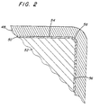
- FIG 2. shows a schematic of an enlarged cross-section of a portion of a substrate used in Test A after a TiCN coating had been applied in the test.
- a coating of TiCN 48 was deposited on a layer of TiN 50 which had been applied to the tungsten carbide substrate's 52 rake face 54 , flank face 56 , and cutting edge 58 at the juncture of the rake and flank faces prior to the start of the test.
- the TiCN coating thickness measurements were made on the rake face at a distance of 1 millimeter from the cutting edge.
- the results of the TiCN coating thickness measurements for Tests A and B are shown in Table 3. These results show that the average coating thickness increased from about 2.8 microns for the samples processed by the conventional MT CVD method to about 9.8 microns for the samples processed according to an embodiment of the present invention. Additionally, the variability of coating thickness as measured by the coefficient of variability (C.O.V.), which is the standard deviation of the thickness measurements divided by the mean thickness measurement, was reduced from 0.54 in Test B for the samples processed by the conventional MT CVD method to 0.28 in Test A for the samples processed according to an embodiment of the present invention.
- C.O.V. coefficient of variability
- Test A which was conducted in accordance with an embodiment of the present invention, the addition of a predetermined amount of HCl to a MT CVD deposition process gas that also contained predetermined amounts of CH 3 , TiCl 4 , H 2 , and N 2 resulted in significant improvements to the both the TiCN coating deposition rate and the uniformity of the TiCN coating thickness on substrates located throughout the reaction chamber.
- Test C a test of an embodiment of the present invention was conducted in which the composition of the deposition process gas was varied from that used in Test A. All other conditions were essentially the same as those used for Test A as were the substrate composition, geometry, and surface condition.
- the deposition process gas composition for Test C is given in Table 1 and the MT CVD operational parameters are given in Table 2.
- the results of thickness measurements of the TiCN coatings deposited in Test C appear in Table 3. These results show that the practice of an embodiment of the present invention in Test C improved the deposition rates and coating uniformity over that which was obtained in Test B by a conventional MT CVD technique.
- Test D a test of an embodiment of the present invention was conducted in which a temperature gradient was used in the reaction chamber so that the substrates proximal to the entrance location of the deposition process gas into the reaction chamber were heated to a reaction temperature about 40°C lower than the reaction temperature of those substrates most remote from the deposition process gas entrance. All other conditions were essentially the same as those used for Test A as were the substrate composition, geometry, and surface condition.
- the deposition process gas composition for Test D is given in Table 1 and the MT CVD operational parameters are given in Table 2.
- Test E an embodiment of the present invention employing a temperature gradient as in Test D was practiced but the reaction pressure was decreased from the 120 Torr (16 kN m -2 ) level used in Test D to 90 Torr (12 kN m -2 ) in Test E. All other conditions were essentially the same as were used for Test D as were the substrate composition, geometry, and surface condition.
- the deposition process gas composition for Test E is given in Table 1 and the MT CVD operational parameters are given in Table 2.
- the results of thickness measurements of the TiCN coatings deposited in Test E appear in Table 3.
- the results of Test E in terms of deposition rate and coating uniformity are comparable to those obtained for Test D and superior to those obtained in Test B by a conventional MT CVD technique.
- Test F an embodiment of the present invention was practiced in which the operational parameters were similar to those used in Test E except that the composition of the deposition process gas was changed to lower the concentrations of TiCl 4 and CH 3 CN. Also, in addition to using substrates having the composition, geometry, and surface condition as were used for Test D, additional substrates of the ceramic Si 3 N 4 - 1% yttria (Y 2 O 3 ) - 1% magnesia (MgO) were included (see U.S. Pat. No. 5,382,273). These ceramic substrates had a geometry of Kennametal Style SNGA433T and had not been precoated with TiN. The surfaces of these ceramic substrates were cleaned by conventional techniques known to those skilled in the art prior to use in Test F.
- the deposition process gas composition for Test F is given in Table 1 and the MT CVD operational parameters are given in Table 2.
- the results of thickness measurements of the TiCN coatings deposited on the cemented carbide inserts in Test F appear in Table 3. Although the ceramic Si 3 N 4 substrates were also found to be coated with TiCN, no coating thickness measurements were taken. The results of the thickness measurements on the cemented carbide inserts show that the deposition rate of the TiCN was lower than that obtained in Test E but were still significantly greater than those obtained in Test B by a conventional MT CVD technique. The results of Test F in terms of coating uniformity are comparable to those obtained for Test D and superior to those obtained in Test B by a conventional MT CVD technique.
- Test G demonstrates one way in which the present invention can be used intermittently with other coating techniques to construct on a substrate a multilayer coating comprised of a variety of coating materials.
- Test G an embodiment of the present invention was used in conjunction with conventional CVD and MT CVD coating deposition techniques to form a multilayer coating on a previously uncoated cemented tungsten carbide insert.
- the layers deposited in Test G are listed in Table 4. Three of these layers, layers 2, 4, and 6, were deposited using an embodiment of the present invention which employed conditions similar to those used in Test A except that the reaction pressure in Test G was 90 Torr (12 kN m -2 ) instead of the 120 Torr (16 kN m -2 ) used in Test A.
- the deposition process gas composition used in depositing layers 2, 4, and 6 in Test G is given in Table 1 and the MT CVD operational parameters for these layers are given in Table 2.
- Test G was conducted in the following manner.
- the substrates were heated to a reaction temperature of 870°C in the manner and in the reaction vessel described above for Test A.
- a conventional CVD method was then used to deposit the TiN of layer 1.
- a MT CVD layer of TiCN, layer 2 was then applied according to an embodiment of the present invention in the manner described in Test A.
- a conventional CVD method was then used to deposit the TiN of layer 3.
- a MT CVD layer of TiCN, layer 4 was then applied according to an embodiment of the present invention in the same manner as was used for layer 2.
- a conventional CVD method was then used to deposit the TiN of layer 5.
- a MT CVD layer of TiCN, layer 6, was then applied according to an embodiment of the present invention in the same manner as was used for layers 2 and 4.
- the reaction temperature was then increased and conventional CVD methods were used to deposit the TiCN, TiC, Al 2 O 3 , and TiN coatings of layers 7 through 9.
- Thickness measurements were made on TiCN layers 2 and 4 which were deposited in Test G by an embodiment of the present invention. The results of these thickness measurements appear in Table 5. Comparing Table 5 with Table 3, it is clear that the uniformity of the TiCN coating throughout reaction chamber is similar to that achieved in Test A and superior to that obtained in Test B by a conventional MT CVD technique.
- Table 6 contains a comparison of the TiCN deposition rates achieved in Tests A through G. The results also show that the deposition rate of the TiCN in layers 2 and 4 of Test G, although lower than that obtained in Test A, were still significantly greater than that obtained in Test B by a conventional MT CVD technique.
Applications Claiming Priority (3)
| Application Number | Priority Date | Filing Date | Title |
|---|---|---|---|
| US09/261,001 US6146697A (en) | 1999-03-02 | 1999-03-02 | MT CVD process |
| US261001 | 1999-03-02 | ||
| PCT/US2000/004682 WO2000052224A1 (en) | 1999-03-02 | 2000-02-24 | Mt cvd process |
Publications (2)
| Publication Number | Publication Date |
|---|---|
| EP1157143A1 EP1157143A1 (en) | 2001-11-28 |
| EP1157143B1 true EP1157143B1 (en) | 2002-11-06 |
Family
ID=22991551
Family Applications (1)
| Application Number | Title | Priority Date | Filing Date |
|---|---|---|---|
| EP00913591A Revoked EP1157143B1 (en) | 1999-03-02 | 2000-02-24 | Mt cvd process |
Country Status (11)
| Country | Link |
|---|---|
| US (1) | US6146697A (ja) |
| EP (1) | EP1157143B1 (ja) |
| JP (2) | JP4728486B2 (ja) |
| KR (1) | KR100661977B1 (ja) |
| CN (1) | CN1342216A (ja) |
| AT (1) | ATE227358T1 (ja) |
| CA (1) | CA2360713A1 (ja) |
| DE (2) | DE1157143T1 (ja) |
| ES (1) | ES2184704T3 (ja) |
| IL (1) | IL144500A0 (ja) |
| WO (1) | WO2000052224A1 (ja) |
Cited By (2)
| Publication number | Priority date | Publication date | Assignee | Title |
|---|---|---|---|---|
| DE102012016485A1 (de) | 2011-08-29 | 2013-02-28 | Kennametal Inc. | Schneideinsatz mit einer Titanoxycarbonitrid-Beschichtung und Verfahren zur Herstellung desselben |
| US8734070B2 (en) | 2010-10-20 | 2014-05-27 | Kennametal Inc. | Toolholder with externally-mounted dynamic absorber |
Families Citing this family (18)
| Publication number | Priority date | Publication date | Assignee | Title |
|---|---|---|---|---|
| US6146697A (en) * | 1999-03-02 | 2000-11-14 | Kennametal Inc. | MT CVD process |
| US6352014B1 (en) * | 1999-12-15 | 2002-03-05 | International Business Machines Corporation | Method for making punches using multi-layer ceramic technology |
| US6533910B2 (en) * | 2000-12-29 | 2003-03-18 | Lam Research Corporation | Carbonitride coated component of semiconductor processing equipment and method of manufacturing thereof |
| JP2002289616A (ja) * | 2001-03-28 | 2002-10-04 | Mitsubishi Heavy Ind Ltd | 成膜方法及び成膜装置 |
| DE10122329B4 (de) * | 2001-05-08 | 2004-06-03 | Tinox Gmbh | Wärmetauscher-Vorrichtung mit einer oberflächenbeschichteten Wand, die Medium 1 von Medium 2 trennt |
| KR20030052468A (ko) * | 2001-12-21 | 2003-06-27 | 한국야금 주식회사 | 내마모성 공구용 박막 및 이를 이용하는 피복부재 |
| ATE518971T1 (de) * | 2005-11-17 | 2011-08-15 | Boehlerit Gmbh & Co Kg | Titancarbonitridschicht und verfahren zum herstellen einer titancarbonitridschicht |
| AT503050B1 (de) * | 2005-11-17 | 2007-09-15 | Boehlerit Gmbh & Co Kg | Metallcarbonitridschicht |
| KR100791112B1 (ko) * | 2005-12-23 | 2008-01-04 | 한국야금 주식회사 | 절삭공구용 고경도 cvd 다원소 복합막 |
| JP4753249B2 (ja) * | 2006-01-13 | 2011-08-24 | 株式会社神戸製鋼所 | ガラス成形用金型 |
| EP1897970B2 (en) * | 2006-09-05 | 2016-06-15 | Tungaloy Corporation | Coated cutting tool and method for producing the same |
| JP6022228B2 (ja) | 2011-09-14 | 2016-11-09 | 株式会社日立国際電気 | 半導体装置の製造方法、基板処理方法、基板処理装置およびプログラム |
| AT13091U1 (de) * | 2012-02-27 | 2013-06-15 | Ceratizit Austria Gmbh | Verfahren zur Herstellung einer Hartstoffschicht auf einem Substrat, Hartstoffschicht sowie Zerspanwerkzeug |
| KR101456685B1 (ko) | 2013-03-08 | 2014-11-12 | 부산대학교 산학협력단 | 금속 부품의 고경도 표면코팅 방법 |
| EP3856950A1 (en) | 2018-09-28 | 2021-08-04 | Corning Incorporated | Low temperature methods for depositing inorganic particles on a metal substrate and articles produced by the same |
| US11464102B2 (en) * | 2018-10-06 | 2022-10-04 | Fermi Research Alliance, Llc | Methods and systems for treatment of superconducting materials to improve low field performance |
| JP7425990B2 (ja) | 2020-03-19 | 2024-02-01 | 三菱マテリアル株式会社 | 表面被覆切削工具の製造方法 |
| CN116162918B (zh) * | 2023-04-26 | 2023-07-14 | 赣州澳克泰工具技术有限公司 | 一种高硬度高韧性的刀具涂层及制备方法 |
Family Cites Families (13)
| Publication number | Priority date | Publication date | Assignee | Title |
|---|---|---|---|---|
| US3846162A (en) * | 1968-10-21 | 1974-11-05 | Texas Instruments Inc | Metal carbonitride coatings |
| US4196233A (en) * | 1974-02-07 | 1980-04-01 | Ciba-Geigy Corporation | Process for coating inorganic substrates with carbides, nitrides and/or carbonitrides |
| JP3109272B2 (ja) * | 1992-08-04 | 2000-11-13 | 三菱マテリアル株式会社 | 耐欠損性および耐摩耗性にすぐれた表面被覆炭窒化チタン基サーメット製切削工具 |
| US5436071A (en) * | 1990-01-31 | 1995-07-25 | Mitsubishi Materials Corporation | Cermet cutting tool and process for producing the same |
| JP2585470B2 (ja) * | 1991-01-14 | 1997-02-26 | 日本碍子株式会社 | ハニカム構造体押出用口金の製造方法 |
| DE4239234A1 (de) * | 1992-11-21 | 1994-06-09 | Krupp Widia Gmbh | Werkzeug und Verfahren zur Beschichtung eines Werkzeuggrundkörpers |
| US5681651A (en) * | 1992-11-27 | 1997-10-28 | Mitsubishi Materials Corporation | Multilayer coated hard alloy cutting tool |
| SE514737C2 (sv) * | 1994-03-22 | 2001-04-09 | Sandvik Ab | Belagt skärverktyg av hårdmetall |
| US5652045A (en) * | 1994-10-20 | 1997-07-29 | Mitsubishi Materials Corporation | Coated tungsten carbide-based cemented carbide blade member |
| US5786069A (en) * | 1995-09-01 | 1998-07-28 | Sandvik Ab | Coated turning insert |
| JPH09310179A (ja) * | 1996-05-20 | 1997-12-02 | Mitsubishi Materials Corp | 減圧式縦型化学蒸着装置および化学蒸着方法 |
| SE510778C2 (sv) * | 1996-07-11 | 1999-06-21 | Sandvik Ab | Belagt skär för finfräsning av grått gjutjärn |
| US6146697A (en) * | 1999-03-02 | 2000-11-14 | Kennametal Inc. | MT CVD process |
-
1999
- 1999-03-02 US US09/261,001 patent/US6146697A/en not_active Expired - Lifetime
-
2000
- 2000-02-24 AT AT00913591T patent/ATE227358T1/de not_active IP Right Cessation
- 2000-02-24 CA CA002360713A patent/CA2360713A1/en not_active Abandoned
- 2000-02-24 JP JP2000602831A patent/JP4728486B2/ja not_active Expired - Fee Related
- 2000-02-24 DE DE1157143T patent/DE1157143T1/de active Pending
- 2000-02-24 DE DE60000725T patent/DE60000725T2/de not_active Expired - Lifetime
- 2000-02-24 WO PCT/US2000/004682 patent/WO2000052224A1/en active IP Right Grant
- 2000-02-24 EP EP00913591A patent/EP1157143B1/en not_active Revoked
- 2000-02-24 IL IL14450000A patent/IL144500A0/xx unknown
- 2000-02-24 KR KR1020017011047A patent/KR100661977B1/ko not_active IP Right Cessation
- 2000-02-24 ES ES00913591T patent/ES2184704T3/es not_active Expired - Lifetime
- 2000-02-24 CN CN00804441A patent/CN1342216A/zh active Pending
-
2011
- 2011-02-10 JP JP2011026981A patent/JP2011137238A/ja active Pending
Cited By (3)
| Publication number | Priority date | Publication date | Assignee | Title |
|---|---|---|---|---|
| US8734070B2 (en) | 2010-10-20 | 2014-05-27 | Kennametal Inc. | Toolholder with externally-mounted dynamic absorber |
| DE102012016485A1 (de) | 2011-08-29 | 2013-02-28 | Kennametal Inc. | Schneideinsatz mit einer Titanoxycarbonitrid-Beschichtung und Verfahren zur Herstellung desselben |
| US8524360B2 (en) | 2011-08-29 | 2013-09-03 | Kennametal Inc. | Cutting insert with a titanium oxycarbonitride coating and method for making the same |
Also Published As
| Publication number | Publication date |
|---|---|
| US6146697A (en) | 2000-11-14 |
| CA2360713A1 (en) | 2000-09-08 |
| EP1157143A1 (en) | 2001-11-28 |
| JP4728486B2 (ja) | 2011-07-20 |
| DE60000725T2 (de) | 2003-08-21 |
| DE60000725D1 (de) | 2002-12-12 |
| IL144500A0 (en) | 2002-05-23 |
| WO2000052224A1 (en) | 2000-09-08 |
| CN1342216A (zh) | 2002-03-27 |
| ATE227358T1 (de) | 2002-11-15 |
| DE1157143T1 (de) | 2002-07-04 |
| JP2002538308A (ja) | 2002-11-12 |
| JP2011137238A (ja) | 2011-07-14 |
| KR100661977B1 (ko) | 2006-12-27 |
| ES2184704T3 (es) | 2003-04-16 |
| KR20010105364A (ko) | 2001-11-28 |
Similar Documents
| Publication | Publication Date | Title |
|---|---|---|
| EP1157143B1 (en) | Mt cvd process | |
| CA2077205C (en) | Titanium carbonitride coated stratified substrate | |
| US5766782A (en) | Aluminum oxide coated cutting tool and method of manufacturing thereof | |
| US5674564A (en) | Alumina-coated sintered body | |
| US6156383A (en) | Alumina coated tool and production method thereof | |
| US5968595A (en) | Oxide coated cutting tool with increased wear resistance and method of manufacture thereof | |
| US5654035A (en) | Method of coating a body with an α-alumina coating | |
| US5915162A (en) | Coated cutting tool and a process for the production of the same | |
| US5980988A (en) | Alumina coated cutting tool | |
| US8343620B2 (en) | Alumina coated grade | |
| US4965140A (en) | Composite coatings on refractory substrates | |
| US4988564A (en) | Metal carbide, nitride, or carbonitride whiskers coated with metal carbides, nitrides, carbonitrides, or oxides | |
| US20020122701A1 (en) | Oxide coated cutting tool | |
| US6040012A (en) | Process for the preparation by chemical vapor deposition (CVD) of a Ti-A1-N based multilayer coating | |
| JPS6115149B2 (ja) | ||
| US4943450A (en) | Method for depositing nitride-based composite coatings by CVD | |
| EP0045291B1 (en) | Method of making a coated cemented carbide body and body produced in such a manner | |
| CA2765645A1 (en) | Coated substrates and methods of making same | |
| JP2876132B2 (ja) | 被覆切削工具 | |
| EP1262576B1 (en) | CVD Al2O3 coated cutting tool | |
| JP2876130B2 (ja) | 被覆切削工具 | |
| US6413628B1 (en) | Titanium carbonitride coated cemented carbide and cutting inserts made from the same | |
| WO2023088866A1 (en) | Moderate temperature cvd alpha alumina coating | |
| Sjöstrand | Limitations of present CVD technologies |
Legal Events
| Date | Code | Title | Description |
|---|---|---|---|
| PUAI | Public reference made under article 153(3) epc to a published international application that has entered the european phase |
Free format text: ORIGINAL CODE: 0009012 |
|
| 17P | Request for examination filed |
Effective date: 20010814 |
|
| AK | Designated contracting states |
Kind code of ref document: A1 Designated state(s): AT BE CH CY DE DK ES FI FR GB GR IE IT LI LU MC NL PT SE |
|
| EL | Fr: translation of claims filed | ||
| TCAT | At: translation of patent claims filed | ||
| 17Q | First examination report despatched |
Effective date: 20020128 |
|
| GRAG | Despatch of communication of intention to grant |
Free format text: ORIGINAL CODE: EPIDOS AGRA |
|
| GRAG | Despatch of communication of intention to grant |
Free format text: ORIGINAL CODE: EPIDOS AGRA |
|
| GRAG | Despatch of communication of intention to grant |
Free format text: ORIGINAL CODE: EPIDOS AGRA |
|
| GRAH | Despatch of communication of intention to grant a patent |
Free format text: ORIGINAL CODE: EPIDOS IGRA |
|
| DET | De: translation of patent claims | ||
| GRAH | Despatch of communication of intention to grant a patent |
Free format text: ORIGINAL CODE: EPIDOS IGRA |
|
| GRAA | (expected) grant |
Free format text: ORIGINAL CODE: 0009210 |
|
| AK | Designated contracting states |
Kind code of ref document: B1 Designated state(s): AT BE CH CY DE DK ES FI FR GB GR IE IT LI LU MC NL PT SE |
|
| PG25 | Lapsed in a contracting state [announced via postgrant information from national office to epo] |
Ref country code: NL Free format text: LAPSE BECAUSE OF FAILURE TO SUBMIT A TRANSLATION OF THE DESCRIPTION OR TO PAY THE FEE WITHIN THE PRESCRIBED TIME-LIMIT Effective date: 20021106 Ref country code: FI Free format text: LAPSE BECAUSE OF FAILURE TO SUBMIT A TRANSLATION OF THE DESCRIPTION OR TO PAY THE FEE WITHIN THE PRESCRIBED TIME-LIMIT Effective date: 20021106 Ref country code: BE Free format text: LAPSE BECAUSE OF FAILURE TO SUBMIT A TRANSLATION OF THE DESCRIPTION OR TO PAY THE FEE WITHIN THE PRESCRIBED TIME-LIMIT Effective date: 20021106 Ref country code: GR Free format text: LAPSE BECAUSE OF FAILURE TO SUBMIT A TRANSLATION OF THE DESCRIPTION OR TO PAY THE FEE WITHIN THE PRESCRIBED TIME-LIMIT Effective date: 20021106 |
|
| REF | Corresponds to: |
Ref document number: 227358 Country of ref document: AT Date of ref document: 20021115 Kind code of ref document: T |
|
| REG | Reference to a national code |
Ref country code: GB Ref legal event code: FG4D |
|
| REG | Reference to a national code |
Ref country code: CH Ref legal event code: EP |
|
| REG | Reference to a national code |
Ref country code: IE Ref legal event code: FG4D |
|
| REG | Reference to a national code |
Ref country code: CH Ref legal event code: NV Representative=s name: MOINAS & SAVOYE SA |
|
| REF | Corresponds to: |
Ref document number: 60000725 Country of ref document: DE Date of ref document: 20021212 |
|
| PGFP | Annual fee paid to national office [announced via postgrant information from national office to epo] |
Ref country code: AT Payment date: 20030107 Year of fee payment: 4 |
|
| PG25 | Lapsed in a contracting state [announced via postgrant information from national office to epo] |
Ref country code: PT Free format text: LAPSE BECAUSE OF FAILURE TO SUBMIT A TRANSLATION OF THE DESCRIPTION OR TO PAY THE FEE WITHIN THE PRESCRIBED TIME-LIMIT Effective date: 20030206 Ref country code: DK Free format text: LAPSE BECAUSE OF FAILURE TO SUBMIT A TRANSLATION OF THE DESCRIPTION OR TO PAY THE FEE WITHIN THE PRESCRIBED TIME-LIMIT Effective date: 20030206 |
|
| PGFP | Annual fee paid to national office [announced via postgrant information from national office to epo] |
Ref country code: ES Payment date: 20030220 Year of fee payment: 4 |
|
| PG25 | Lapsed in a contracting state [announced via postgrant information from national office to epo] |
Ref country code: CY Free format text: LAPSE BECAUSE OF FAILURE TO SUBMIT A TRANSLATION OF THE DESCRIPTION OR TO PAY THE FEE WITHIN THE PRESCRIBED TIME-LIMIT Effective date: 20030224 Ref country code: IE Free format text: LAPSE BECAUSE OF NON-PAYMENT OF DUE FEES Effective date: 20030224 |
|
| PG25 | Lapsed in a contracting state [announced via postgrant information from national office to epo] |
Ref country code: MC Free format text: LAPSE BECAUSE OF NON-PAYMENT OF DUE FEES Effective date: 20030228 |
|
| NLV1 | Nl: lapsed or annulled due to failure to fulfill the requirements of art. 29p and 29m of the patents act | ||
| REG | Reference to a national code |
Ref country code: ES Ref legal event code: FG2A Ref document number: 2184704 Country of ref document: ES Kind code of ref document: T3 |
|
| PGFP | Annual fee paid to national office [announced via postgrant information from national office to epo] |
Ref country code: LU Payment date: 20030512 Year of fee payment: 4 |
|
| ET | Fr: translation filed | ||
| PLBQ | Unpublished change to opponent data |
Free format text: ORIGINAL CODE: EPIDOS OPPO |
|
| PLBI | Opposition filed |
Free format text: ORIGINAL CODE: 0009260 |
|
| PLAX | Notice of opposition and request to file observation + time limit sent |
Free format text: ORIGINAL CODE: EPIDOSNOBS2 |
|
| 26 | Opposition filed |
Opponent name: SANDVIK AB Effective date: 20030805 |
|
| REG | Reference to a national code |
Ref country code: IE Ref legal event code: MM4A |
|
| PLAX | Notice of opposition and request to file observation + time limit sent |
Free format text: ORIGINAL CODE: EPIDOSNOBS2 |
|
| PGFP | Annual fee paid to national office [announced via postgrant information from national office to epo] |
Ref country code: FR Payment date: 20040202 Year of fee payment: 5 |
|
| PGFP | Annual fee paid to national office [announced via postgrant information from national office to epo] |
Ref country code: SE Payment date: 20040203 Year of fee payment: 5 |
|
| PG25 | Lapsed in a contracting state [announced via postgrant information from national office to epo] |
Ref country code: GB Free format text: LAPSE BECAUSE OF NON-PAYMENT OF DUE FEES Effective date: 20040224 Ref country code: AT Free format text: LAPSE BECAUSE OF NON-PAYMENT OF DUE FEES Effective date: 20040224 |
|
| PG25 | Lapsed in a contracting state [announced via postgrant information from national office to epo] |
Ref country code: ES Free format text: LAPSE BECAUSE OF NON-PAYMENT OF DUE FEES Effective date: 20040225 |
|
| PG25 | Lapsed in a contracting state [announced via postgrant information from national office to epo] |
Ref country code: LI Free format text: LAPSE BECAUSE OF NON-PAYMENT OF DUE FEES Effective date: 20040229 Ref country code: CH Free format text: LAPSE BECAUSE OF NON-PAYMENT OF DUE FEES Effective date: 20040229 |
|
| PLBB | Reply of patent proprietor to notice(s) of opposition received |
Free format text: ORIGINAL CODE: EPIDOSNOBS3 |
|
| GBPC | Gb: european patent ceased through non-payment of renewal fee |
Effective date: 20040224 |
|
| REG | Reference to a national code |
Ref country code: CH Ref legal event code: PL |
|
| PG25 | Lapsed in a contracting state [announced via postgrant information from national office to epo] |
Ref country code: IT Free format text: LAPSE BECAUSE OF NON-PAYMENT OF DUE FEES Effective date: 20050224 |
|
| PG25 | Lapsed in a contracting state [announced via postgrant information from national office to epo] |
Ref country code: SE Free format text: LAPSE BECAUSE OF NON-PAYMENT OF DUE FEES Effective date: 20050225 |
|
| REG | Reference to a national code |
Ref country code: ES Ref legal event code: FD2A Effective date: 20040225 |
|
| EUG | Se: european patent has lapsed | ||
| PG25 | Lapsed in a contracting state [announced via postgrant information from national office to epo] |
Ref country code: FR Free format text: LAPSE BECAUSE OF NON-PAYMENT OF DUE FEES Effective date: 20051031 |
|
| REG | Reference to a national code |
Ref country code: FR Ref legal event code: ST Effective date: 20051031 |
|
| PLAB | Opposition data, opponent's data or that of the opponent's representative modified |
Free format text: ORIGINAL CODE: 0009299OPPO |
|
| R26 | Opposition filed (corrected) |
Opponent name: SANDVIK AB Effective date: 20030805 |
|
| RDAF | Communication despatched that patent is revoked |
Free format text: ORIGINAL CODE: EPIDOSNREV1 |
|
| APBM | Appeal reference recorded |
Free format text: ORIGINAL CODE: EPIDOSNREFNO |
|
| APBP | Date of receipt of notice of appeal recorded |
Free format text: ORIGINAL CODE: EPIDOSNNOA2O |
|
| APAH | Appeal reference modified |
Free format text: ORIGINAL CODE: EPIDOSCREFNO |
|
| APBQ | Date of receipt of statement of grounds of appeal recorded |
Free format text: ORIGINAL CODE: EPIDOSNNOA3O |
|
| APBU | Appeal procedure closed |
Free format text: ORIGINAL CODE: EPIDOSNNOA9O |
|
| PLAB | Opposition data, opponent's data or that of the opponent's representative modified |
Free format text: ORIGINAL CODE: 0009299OPPO |
|
| R26 | Opposition filed (corrected) |
Opponent name: SANDVIK AB Effective date: 20030805 |
|
| PGFP | Annual fee paid to national office [announced via postgrant information from national office to epo] |
Ref country code: DE Payment date: 20140417 Year of fee payment: 15 |
|
| REG | Reference to a national code |
Ref country code: DE Ref legal event code: R119 Ref document number: 60000725 Country of ref document: DE |
|
| PG25 | Lapsed in a contracting state [announced via postgrant information from national office to epo] |
Ref country code: DE Free format text: LAPSE BECAUSE OF NON-PAYMENT OF DUE FEES Effective date: 20150901 |
|
| RDAD | Information modified related to despatch of communication that patent is revoked |
Free format text: ORIGINAL CODE: EPIDOSCREV1 |
|
| REG | Reference to a national code |
Ref country code: DE Ref legal event code: R064 Ref document number: 60000725 Country of ref document: DE Ref country code: DE Ref legal event code: R103 Ref document number: 60000725 Country of ref document: DE |
|
| RDAG | Patent revoked |
Free format text: ORIGINAL CODE: 0009271 |
|
| STAA | Information on the status of an ep patent application or granted ep patent |
Free format text: STATUS: PATENT REVOKED |
|
| 27W | Patent revoked |
Effective date: 20160422 |
|
| REG | Reference to a national code |
Ref country code: SE Ref legal event code: ECNC |
|
| REG | Reference to a national code |
Ref country code: AT Ref legal event code: MA03 Ref document number: 227358 Country of ref document: AT Kind code of ref document: T Effective date: 20160422 |