EP1154479A2 - Grille à lignes multiples utilisée pour des applications dans des domaines d encapsulation et d essayage - Google Patents
Grille à lignes multiples utilisée pour des applications dans des domaines d encapsulation et d essayage Download PDFInfo
- Publication number
- EP1154479A2 EP1154479A2 EP01111638A EP01111638A EP1154479A2 EP 1154479 A2 EP1154479 A2 EP 1154479A2 EP 01111638 A EP01111638 A EP 01111638A EP 01111638 A EP01111638 A EP 01111638A EP 1154479 A2 EP1154479 A2 EP 1154479A2
- Authority
- EP
- European Patent Office
- Prior art keywords
- multiple line
- line grid
- bumps
- via holes
- connection lines
- Prior art date
- Legal status (The legal status is an assumption and is not a legal conclusion. Google has not performed a legal analysis and makes no representation as to the accuracy of the status listed.)
- Withdrawn
Links
Images

Classifications
-
- H—ELECTRICITY
- H01—ELECTRIC ELEMENTS
- H01L—SEMICONDUCTOR DEVICES NOT COVERED BY CLASS H10
- H01L25/00—Assemblies consisting of a plurality of individual semiconductor or other solid state devices ; Multistep manufacturing processes thereof
-
- H—ELECTRICITY
- H01—ELECTRIC ELEMENTS
- H01L—SEMICONDUCTOR DEVICES NOT COVERED BY CLASS H10
- H01L23/00—Details of semiconductor or other solid state devices
- H01L23/48—Arrangements for conducting electric current to or from the solid state body in operation, e.g. leads, terminal arrangements ; Selection of materials therefor
- H01L23/488—Arrangements for conducting electric current to or from the solid state body in operation, e.g. leads, terminal arrangements ; Selection of materials therefor consisting of soldered or bonded constructions
- H01L23/498—Leads, i.e. metallisations or lead-frames on insulating substrates, e.g. chip carriers
- H01L23/49811—Additional leads joined to the metallisation on the insulating substrate, e.g. pins, bumps, wires, flat leads
- H01L23/49816—Spherical bumps on the substrate for external connection, e.g. ball grid arrays [BGA]
-
- H—ELECTRICITY
- H01—ELECTRIC ELEMENTS
- H01L—SEMICONDUCTOR DEVICES NOT COVERED BY CLASS H10
- H01L23/00—Details of semiconductor or other solid state devices
- H01L23/48—Arrangements for conducting electric current to or from the solid state body in operation, e.g. leads, terminal arrangements ; Selection of materials therefor
- H01L23/488—Arrangements for conducting electric current to or from the solid state body in operation, e.g. leads, terminal arrangements ; Selection of materials therefor consisting of soldered or bonded constructions
- H01L23/498—Leads, i.e. metallisations or lead-frames on insulating substrates, e.g. chip carriers
- H01L23/49827—Via connections through the substrates, e.g. pins going through the substrate, coaxial cables
-
- H—ELECTRICITY
- H01—ELECTRIC ELEMENTS
- H01L—SEMICONDUCTOR DEVICES NOT COVERED BY CLASS H10
- H01L2924/00—Indexing scheme for arrangements or methods for connecting or disconnecting semiconductor or solid-state bodies as covered by H01L24/00
- H01L2924/0001—Technical content checked by a classifier
- H01L2924/0002—Not covered by any one of groups H01L24/00, H01L24/00 and H01L2224/00
Definitions
- the present invention relates to a multiple line grid (MLG) for use in a packaging or a testing application and a method for the manufacture thereof; and, more particularly, to the MLG incorporated in a wafer level package to allow I/O pads to be redistributed from a peripheral array to an area array.
- MLG multiple line grid
- flip-chip attachment method instead of attaching a semiconductor chip to a lead frame in a package, an array of solder bumps is formed on the surface of the chip, using either an evaporation method or an electrodeposition method.
- an object of the present invention to provide a novel structure capable of allowing an I/O redistribution from a peripheral array to an area array in interconnecting a semiconductor chip and another electronic circuit.
- a multiple line grid including:
- the present invention discloses a multiple line grid (MLG) for interconnecting an electronic component, e.g., a printed circuit board or the like, with a semiconductor chip having a number of I/O pads disposed on the periphery thereof.
- MLG multiple line grid
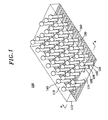
- Fig. 1 shows the MLG 100 including a body 110 having a top and a bottom surfaces 112, 114, a plurality of via holes 120, each of the via holes extending from the top surface 112 to the bottom surface 114 of the body 110, an identical number of connection lines, upper and lower bumps 130,140,150, as that of the via holes 120, each connection line connecting one lower bump to one end of a via hole, and each upper bump 140 being formed at the opposite end from the end of the via hole connected to each of the lower bumps through the connecting line 130.
- the body 110 is made of an insulating material, e.g., a ceramic, a polymer or a composite of ceramic and polymer.
- Each of the via holes 120 extends through the body 110 with a first end 122 exposed on the top surface 112 of the body 110 and a second opposite end 124 exposed on the bottom surface 114 thereof.
- Each of the via holes 120 includes a conductor 126 made of either a metal, e.g., Cu, Ni and Au, or an Ag-compound, e.g., Ag-Pt and Ag-Pd, containing glass components.
- the conductor 126 covers the inner surfaces of the via holes 120 and encompasses the first and the second end 122, 124 thereof, as shown in Fig. 3. Additionally, each of the via holes 120 covered by the conductor 126 may be filled with the conductor 126 or an electrically insulating material.
- each of the upper bumps 140 for securing the MLG 100 on, e.g., a printed circuit board, having connection pads thereon, is provided with a solder paste and is placed on the top surface 112 of the body 110 with a direct contact to the first end 122 of the corresponding via hole 120.
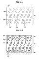
- the upper bumps 140 are disposed in the central region of the top surface 112 of the body 110 to form an array 162, the array 162 having a configuration such that all of the upper bumps 140 can be divided into a repetitive alignment of M number of groups 142, each group having N number of upper bumps 140, M, N being integers greater than 1.
- each of the group 142 includes three upper bumps 140, the bumps being regularly spaced apart with a first pitch 164.
- Each of the lower bumps 150 to be used in mounting the multiple line grid 100 on a semiconductor chip having, e.g., connection pads on two opposing sides thereof, is made of, e.g., a solder paste, and is placed on the bottom surface 114 of the body 110. As shown in Fig. 2B, the lower bumps 150 are disposed along the two opposing peripheries/sides of the bottom surface 114 of the body 110 and regularly spaced apart with a second pitch 168 to form two peripheral arrays 166. The first pitch 164 is larger than the second pitch 168.
- connection lines 130 is made of an electrically conducting material and is positioned on the bottom surface 114 of the body 110.
- the connection lines 130 rectilinearly extend in parallel from the second ends 124 of their corresponding via holes 120 to their corresponding lower bumps 150, thereby electrically connecting the conductor 126 of each of the via holes 120 to its corresponding lower bump 150.
- Each of the connection lines 130 is apart from the neighbouring connection lines 130 by the second pitch 168 and two neighbouring connection lines 130 differ in length.
- the insulating body 110 made of an insulating material, e.g., a ceramic, a polymer or a composite of ceramic and polymer, and having the top and the bottom surface 112, 114, is first prepared.
- the via holes 120 are formed to penetrate through the body 110 by using, e.g., a laser drilling or a punching method, wherein each of the via holes 120 is disposed to coincide with the first end of the corresponding connection line 130.
- the conductors 126 are made of an Agcompound, e.g., Ag-Pt and Ag-Pd, containing a glass component if the body 110 is made of Al 2 O 3 , or of a metal, e.g., Cu, Ni or Au, if the body 110 is made of an insulating polymer or a composite of ceramic and polymer.
- an Agcompound e.g., Ag-Pt and Ag-Pd
- a glass component if the body 110 is made of Al 2 O 3
- a metal e.g., Cu, Ni or Au
- connection lines 130 made of an electrical conducting material are formed on the bottom surface 114 of the body 110 by using, e.g., a screenprinting method with a mask and a solder reflow method.
- Each of the connection lines 130 is provided with a first one end thereof positioned at the central area of the body 110 and a second end placed at the peripheral/side area of the body 110, each of the connection lines 130 running parallel to each other.
- the lower bumps 150 are formed with a solder paste by using, e.g., a screen printing method and a solder reflow method, wherein each of the lower bumps 150 is positioned to coincide with the second end of the corresponding connection line 130.
- the upper bumps 140 are formed with a solder paste, e.g., by using a screen printing method and a solder reflow method, wherein the upper bumps 140 are in contact with the via holes 120.
- a step for filling the via holes 120 should be added. This step can be achieved by either filling the via holes 120 with an insulating material, e.g., a solder ink, after the formation of the conductors 126, or filling the via holes 120 with the same material as the upper bumps 140, i.e., the solder paste, during the formation of the upper bumps 140.
- an insulating material e.g., a solder ink
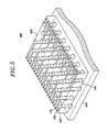
- Fig. 4 is an example of the multiple line grid 100 utilized for packaging an electronic component, e.g., a chip.
- the chip package 200 includes a semiconductor chip 210 having, e.g., two peripheral/side arrays of I/O pads 220, each array having MN/2 I/O pads, and the multiple line grid 100.
- Each of the I/O pads 220 of the semiconductor chip 210 is bonded to the corresponding lower bump 150 of the multiple line grid 100, which, in turn, is electrically connected to the corresponding upper bump 140 through the corresponding connection line 130 and via hole 120.
- the chip package 200 can be mounted on a printed circuit board by using the upper bumps 140 of the multiple line grid 100.
- the multiple line grid 100 of the present invention allows the I/O pads to be easily redistributed, which, in turn, allows the semiconductor chip 210 having I/O pads with a pitch to be electrically connected to another circuitry, e.g., PCB, having a different I/O pad pitch.
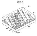
- the ideas presented above can be further utilized in a chip testing application, as schematically illustrated in Fig. 5.
- the multiple line grid 400 shown in Fig 5, further includes a number of reading tips 170, each disposed on a corresponding lower bump 150.
- the multiple line grid 400 is mounted on a testing die 310, e.g., a chip-testing prove card, with the upper bumps 140 mechanically bonded and electrically connected to a testing circuit of the testing die 310, thereby forming a chip-testing device 300.
- the semiconductor chip is coupled to the testing device 300 with the reading tips 170 of the multiple line grid 100 being in contact with I/O pads of the semiconductor chip, in such a way that the semiconductor chip is electrically connected to the testing circuit of the testing die 310. Additionally, a plurality of multiple line grid 100 can be installed on the testing die 310 for testing a plurality of semiconductor chips integrated on a single wafer.
Landscapes
- Engineering & Computer Science (AREA)
- Microelectronics & Electronic Packaging (AREA)
- Physics & Mathematics (AREA)
- Condensed Matter Physics & Semiconductors (AREA)
- General Physics & Mathematics (AREA)
- Computer Hardware Design (AREA)
- Power Engineering (AREA)
- Structures For Mounting Electric Components On Printed Circuit Boards (AREA)
- Testing Or Measuring Of Semiconductors Or The Like (AREA)
- Testing Of Individual Semiconductor Devices (AREA)
- Measuring Leads Or Probes (AREA)
- Printing Elements For Providing Electric Connections Between Printed Circuits (AREA)
Applications Claiming Priority (2)
| Application Number | Priority Date | Filing Date | Title |
|---|---|---|---|
| KR2000025605 | 2000-05-13 | ||
| KR1020000025605A KR20010104147A (ko) | 2000-05-13 | 2000-05-13 | 반도체용 멀티플 라인 그리드와 그의 제조 방법 및 그를이용하여 피시비 보드 상에 반도체 칩을 실장하는 방법 |
Publications (1)
| Publication Number | Publication Date |
|---|---|
| EP1154479A2 true EP1154479A2 (fr) | 2001-11-14 |
Family
ID=19668545
Family Applications (1)
| Application Number | Title | Priority Date | Filing Date |
|---|---|---|---|
| EP01111638A Withdrawn EP1154479A2 (fr) | 2000-05-13 | 2001-05-14 | Grille à lignes multiples utilisée pour des applications dans des domaines d encapsulation et d essayage |
Country Status (5)
| Country | Link |
|---|---|
| US (1) | US20010040297A1 (fr) |
| EP (1) | EP1154479A2 (fr) |
| JP (1) | JP2002031663A (fr) |
| KR (1) | KR20010104147A (fr) |
| CN (1) | CN1324108A (fr) |
Families Citing this family (6)
| Publication number | Priority date | Publication date | Assignee | Title |
|---|---|---|---|---|
| KR100716434B1 (ko) * | 2006-04-17 | 2007-05-10 | 주식회사 파이컴 | 프로브 본딩 방법 및 프로브 카드 제조 방법 |
| US8264085B2 (en) * | 2008-05-05 | 2012-09-11 | Infineon Technologies Ag | Semiconductor device package interconnections |
| CN103187390B (zh) * | 2011-12-31 | 2016-04-13 | 中芯国际集成电路制造(北京)有限公司 | 具有改进排布方式的通孔阵列和具有该阵列的半导体器件 |
| JP6207716B2 (ja) * | 2014-03-06 | 2017-10-04 | 三菱電機株式会社 | 半導体装置 |
| CN107948903B (zh) * | 2017-12-12 | 2020-09-22 | 杭州电子科技大学 | 一种mems麦克风测试系统 |
| WO2022065881A1 (fr) * | 2020-09-28 | 2022-03-31 | 한국산업기술대학교 산학협력단 | Capteur ultrasonore permettant l'établissement d'informations d'empreintes digitales tridimensionnelles |
Family Cites Families (6)
| Publication number | Priority date | Publication date | Assignee | Title |
|---|---|---|---|---|
| JPS62274632A (ja) * | 1986-05-22 | 1987-11-28 | Hitachi Ltd | 検査用小基板およびその使用方法 |
| JP2715793B2 (ja) * | 1992-03-19 | 1998-02-18 | 日本電気株式会社 | 半導体装置及びその製造方法 |
| US5800184A (en) * | 1994-03-08 | 1998-09-01 | International Business Machines Corporation | High density electrical interconnect apparatus and method |
| KR19980059240A (ko) * | 1996-12-31 | 1998-10-07 | 김광호 | 테스트 장치 |
| KR20000007516A (ko) * | 1998-07-03 | 2000-02-07 | 윤종용 | 플립 칩 번-인 테스트 기판 및 이를 이용한 번-인 테스트방법 |
| JP2000040572A (ja) * | 1998-07-23 | 2000-02-08 | Nec Eng Ltd | Lsiパッケージ用ソケット |
-
2000
- 2000-05-13 KR KR1020000025605A patent/KR20010104147A/ko not_active Application Discontinuation
-
2001
- 2001-05-11 US US09/852,644 patent/US20010040297A1/en not_active Abandoned
- 2001-05-14 EP EP01111638A patent/EP1154479A2/fr not_active Withdrawn
- 2001-05-14 JP JP2001143761A patent/JP2002031663A/ja active Pending
- 2001-05-14 CN CN01115712A patent/CN1324108A/zh active Pending
Also Published As
| Publication number | Publication date |
|---|---|
| JP2002031663A (ja) | 2002-01-31 |
| KR20010104147A (ko) | 2001-11-24 |
| CN1324108A (zh) | 2001-11-28 |
| US20010040297A1 (en) | 2001-11-15 |
Similar Documents
| Publication | Publication Date | Title |
|---|---|---|
| US5942795A (en) | Leaded substrate carrier for integrated circuit device and leaded substrate carrier device assembly | |
| US6617695B1 (en) | Semiconductor device and semiconductor module using the same | |
| US6075710A (en) | Low-cost surface-mount compatible land-grid array (LGA) chip scale package (CSP) for packaging solder-bumped flip chips | |
| US4437141A (en) | High terminal count integrated circuit device package | |
| US5901050A (en) | Wired base plate and package for electronic parts | |
| US5045914A (en) | Plastic pad array electronic AC device | |
| KR100231366B1 (ko) | 반도체 패키지 스택 모듈 및 그 제조방법 | |
| US5886876A (en) | Surface-mounted semiconductor package and its manufacturing method | |
| JP3294740B2 (ja) | 半導体装置 | |
| US7038917B2 (en) | Low loss, high density array interconnection | |
| US5177863A (en) | Method of forming integrated leadouts for a chip carrier | |
| EP0377932A2 (fr) | Ensemble de circuits intégrés à semiconducteur | |
| JPH04256343A (ja) | 集積回路用フリップチップパッケージ | |
| US20050248011A1 (en) | Flip chip semiconductor package for testing bump and method of fabricating the same | |
| JP3927783B2 (ja) | 半導体部品 | |
| US6034437A (en) | Semiconductor device having a matrix of bonding pads | |
| US6320249B1 (en) | Multiple line grids incorporating therein circuit elements | |
| US6133134A (en) | Ball grid array integrated circuit package | |
| US6657133B1 (en) | Ball grid array chip capacitor structure | |
| EP1154479A2 (fr) | Grille à lignes multiples utilisée pour des applications dans des domaines d encapsulation et d essayage | |
| KR20030081549A (ko) | 반도체소자 패키지 제조방법 | |
| US6734538B1 (en) | Article comprising a multi-layer electronic package and method therefor | |
| JPS6127667A (ja) | 半導体装置 | |
| KR100367729B1 (ko) | 멀티플 라인 그리드 어레이 패키지 | |
| US7514798B2 (en) | Arrangement for the protection of three-dimensional structures on wafers |
Legal Events
| Date | Code | Title | Description |
|---|---|---|---|
| PUAI | Public reference made under article 153(3) epc to a published international application that has entered the european phase |
Free format text: ORIGINAL CODE: 0009012 |
|
| AK | Designated contracting states |
Kind code of ref document: A2 Designated state(s): AT BE CH CY DE DK ES FI FR GB GR IE IT LI LU MC NL PT SE TR |
|
| AX | Request for extension of the european patent |
Free format text: AL;LT;LV;MK;RO;SI |
|
| STAA | Information on the status of an ep patent application or granted ep patent |
Free format text: STATUS: THE APPLICATION IS DEEMED TO BE WITHDRAWN |
|
| 18D | Application deemed to be withdrawn |
Effective date: 20031202 |