EP1148621A2 - Ladungspumpenanordnung - Google Patents
Ladungspumpenanordnung Download PDFInfo
- Publication number
- EP1148621A2 EP1148621A2 EP01108428A EP01108428A EP1148621A2 EP 1148621 A2 EP1148621 A2 EP 1148621A2 EP 01108428 A EP01108428 A EP 01108428A EP 01108428 A EP01108428 A EP 01108428A EP 1148621 A2 EP1148621 A2 EP 1148621A2
- Authority
- EP
- European Patent Office
- Prior art keywords
- charge pump
- pump
- arrangement according
- output
- pump arrangement
- Prior art date
- Legal status (The legal status is an assumption and is not a legal conclusion. Google has not performed a legal analysis and makes no representation as to the accuracy of the status listed.)
- Withdrawn
Links
Images


Classifications
-
- H—ELECTRICITY
- H02—GENERATION; CONVERSION OR DISTRIBUTION OF ELECTRIC POWER
- H02M—APPARATUS FOR CONVERSION BETWEEN AC AND AC, BETWEEN AC AND DC, OR BETWEEN DC AND DC, AND FOR USE WITH MAINS OR SIMILAR POWER SUPPLY SYSTEMS; CONVERSION OF DC OR AC INPUT POWER INTO SURGE OUTPUT POWER; CONTROL OR REGULATION THEREOF
- H02M3/00—Conversion of DC power input into DC power output
- H02M3/02—Conversion of DC power input into DC power output without intermediate conversion into AC
- H02M3/04—Conversion of DC power input into DC power output without intermediate conversion into AC by static converters
- H02M3/06—Conversion of DC power input into DC power output without intermediate conversion into AC by static converters using resistors or capacitors, e.g. potential divider
- H02M3/07—Conversion of DC power input into DC power output without intermediate conversion into AC by static converters using resistors or capacitors, e.g. potential divider using capacitors charged and discharged alternately by semiconductor devices with control electrode, e.g. charge pumps
- H02M3/073—Charge pumps of the Schenkel-type
Definitions
- the invention relates to a charge pump arrangement in the Preamble of claim 1 mentioned type, that is a charge pump arrangement for adapting a charge pump to the given conditions, with a charge pump, the for generating a charge pump current, a plurality with one another connected pump stages with at least one each Has pump capacitor.
- charge pumps with several Pump stages used on the principle of capacitive Voltage multiplication work and in the simplest case pro Pump stage have a MOS diode and a capacitor.
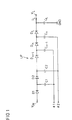
- FIG. 1 shows a known from EP 0 865 149 A2
- Charge pump LP with n pump stages for gradual charge transfer from a power supply on one side, which delivers the supply voltage to a load capacitor CL on the other side of the charge pump LP, on which the increased voltage can be tapped.
- the charge transport to the Load capacitor CL takes place via several diodes D1 - Dn and Pump capacitors C1 - Cn, which are part of each Pump stages are P1 - Pn and together form the power path.
- the diodes D1-Dn are switched through alternately or blocked and the pump capacitors C1 - Cn alternate charged or discharged.
- n worst case denotes the number of pump stages of the charge pump arrangement which must be provided to a minimum in order to dimension the charge pump arrangement for all conceivable permutations of input or output voltages / currents.
- the number of pump stages and thus the pump capacitors n must with the above charge pump for the worst Case dimensioned, that is, for a minimal Supply potential and input potential as well as a maximum required output potential / current. Because this is the worst In the event that occurs very rarely, the charge pump typically oversized for normal operation, which has an unfavorable efficiency. The means that the charge pump produces a lot more power consumed than is actually needed.
- the present invention is therefore based on the object to specify a charge pump arrangement of the type mentioned at the outset, the most optimal in terms of their efficiency is adaptable to the given conditions.
- the pump stages required by the charge pump arrangement are for the current operating point depending on the input or output voltages / currents optimally selected, whereby the efficiency of the charge pump arrangement is optimal can be adjusted.
- the charge pump is one corresponding number of pump stages shortened.
- the said The charge pump is shortened in a very simple manner by bridging or by switching off unnecessary ones Pump stages.
- the output current or the output voltage the charge pump measured by a measuring device and evaluated.
- a control signal is generated, which as Controlled variable is fed back into the charge pump.
- Control signal can be one or more, typically Pump stages not required, switch off or bypass.
- the shutdown or Bridging unneeded pump stages by an AD converter take place from the analog output signal of the charge pump generates a digitized output signal which a downstream up / down counter or one Shift register is fed.
- the shift register or the up / down counter generate from the digitized Output signal a digital control signal.
- this digital control signal can use this digital control signal as an enable signal for control of the individual pump stages are used to turn them off.
- the shortening of the charge pump arrangement is from the beginning of the pump, that is, from the entrance of the charge pump, the simplest realizable, but is in principle at every point of the Charge pump possible.
- the principle of shortening the charge pump is special advantageous for all forms of positive and negative pumps. Charge pumps with energy recovery are provided by the invention Shortening only makes sense.
- the pump capacitors are one or several bridged or switched off pump stages used to buffer the output voltage at the same time become.
- controllable switches can advantageously be simple Transistor elements, for example as MOS transistors, or also as diode elements, in particular as MOS diodes, be trained.
- controllable Realize switches in any other way.
- the control connection is advantageously the controllable one Switch with a boost capacitor and a boost transistor connected in such a way that at the time of a charge flow through this controllable switch its conductivity is increased.
- this measure is imperative to a charge pump to be able to provide with a sufficiently high clock frequency.
- FIG. 2 shows a charge pump arrangement according to the invention, which is a four-stage charge pump LP, that is, a charge pump with four pump stages P1..P4.
- Each of the pump stages P1..P4 has a controllable switch S1..S4 and one Pump capacitor C1..C4 on.
- the controllable switches S1..S4 are connected in series over their load routes, these Series connection between an input 1, in which an input potential VIN can be coupled into the charge pump arrangement and an output 2 at which an output potential VL can be tapped is arranged.
- the pump capacitors are C1..C4 arranged such that one capacitor connection each a node 3 between two controllable switches S1..S4 is connected and the other capacitor connection with a controllable switching unit SE1..SE4 connected is.
- the structure and functioning of these controllable Switching units SE1..SE4 are detailed below described.
- controllable switches Between the series connection of the controllable switches and the Output 2 of the charge pump LP is another controllable one Switch SL arranged. Furthermore, a buffer capacitor is a capacitor CL between output port 2 and a port arranged with a reference potential GND.
- the control connections all controllable switches are S1..S4, SL each with a clock signal F1, F2, which consists of an oscillator clock can be generated in such a way that the controllable Switches S1..S4, SL can be switched on and off alternately are.
- the charge pump arrangement according to FIG. 2 contains a control device RE, a measuring device ME and a Evaluation device AE includes.
- About the measuring device ME which is connected to the output 2 of the charge pump LP, is an output signal, i.e. an output current IL or an output potential VL, tapped from the output of the charge pump LP and measurable.
- the measuring device contains ME an analog-to-digital converter that comes from the analog Output signal IL, VL a digitized output signal generated which of the downstream evaluation device AE is supplied.
- the evaluation device AE contains present embodiment a simple up / Down counter (Up / Down Counter) ADC and a downstream 4-bit counter status indicator ZA.
- the counter reading of the up / down counter ADC becomes this meter reading indicator ZA supplied with one enable signal per bit at its output EN1..EN4 provides that the assigned controllable switching device SE1..SE4 can be fed.
- Each controllable switching device SE1..SE4 is on the input side on the one hand with a first supply line 4, which with a Supply potential is applied, and one second supply line 5, which is connected to the reference potential GND is acted upon, connected.
- Each is controllable on the output side Switching device SE1..SE4, as already mentioned, with the other capacitor connection of the one assigned to it Pump capacitor C1..C4 connected.
- Via a controllable Switches SE1 '.. SE4' within each of the controllable switching devices SE1..SE4 is the named capacitor connection depending on the enable signal EN1..EN4 either with the supply potential VDD or with the reference potential GND can be applied.
- SE4' are also from one that can be derived from the oscillator clock Clock (not shown in Figure 2) driven. As special It proves advantageous if the respective switches SE1..SE4, SE1 '.. SE4' each one pump stage P1..P4 isochronous work or driven by the same clock signal T1, T2 become.
- enable signals EN1..EN4 which are the controllable switches SE1 '.. SE4' of the switching devices SE1..SE4 individual or all P1..P4 pump stages can be switched off and thus bridgeable.
- the charge pump arrangement then has one the number of bridged pump stages P1..P4 reduced number at pump stages P1..P4.
- FIGS. 3 and 4. 3 shows a section of the charge pump arrangement shown in FIG. 2, where only the first two Pump stages P1, P2 were shown.
- the switch S1 of the first pump stage P1 is open and the switch SE1 'is connected to the supply potential VDD, whereby the corresponding capacitor C1 is charged can.
- the switch is S2 closed and the switch SE2 'with the reference potential GND connected, whereby the corresponding capacitor C2 discharges.
- Disconnect pump stages P1..P4 which increases the efficiency Optimize the charge pump arrangement ⁇ significantly leaves.
- the pump stages P1..P4 can be switched off take place from any position of the charge pump arrangement, is from the beginning of the pump or from the end the charge pump LP makes the most sense. Beyond that again to note that through the flexibility that the charge pump arrangement according to the invention offers it possible is also the desired output current or output voltage over a wide range by suitable choice of the pump stages P1..P4 used to be defined.
- the evaluation unit is AE in a simple and therefore advantageous manner by means of an up / down counter ADC has been realized.
- the evaluation device AE could, however, also be a known shift register or realize the like.
- semiconductor integrated circuits often a program-controlled unit, such as for example a microcontroller, a microprocessor, has a signal processor or the like, the Function of the measuring device ME and / or the evaluation device AE advantageously also through this program-controlled Unit can be taken over.
- This programmatically The unit then taps the output signal IL, VL and generates it application-specific, i.e. depending on the programming, the respective enable signals EN1..EN4 for control the controllable switching devices SE1..SE4.
- the charge pump LP is not necessarily like the charge pump LP described above must be built and operated with MOS transistors; the Construction and operation of the charge pump LP is in the Practice depends, among other things, on their function and mode of action be made.
- the controllable ones Switches S1..S4, SL also as MOS diodes or as simple ones Realize diodes.
- can the control connections of the controllable switches S1..S4, SL additional Circuit measures are taken to improve conductivity the respective switch at the moment of a charge flow to increase. Such circuit measures are widely known and can, for example, by a controllable switch S1..S4, SL controlling boost capacitor and boost transistor can be realized.
- the change in length the charge pump by means of a control device can also be advantageous by a control device, for example a processor be made.
- the control signal would be as Control signal trained.
- the charge pump could then, for example to obtain a given pump profile in be controlled appropriately.
Landscapes
- Engineering & Computer Science (AREA)
- Power Engineering (AREA)
- Dc-Dc Converters (AREA)
Abstract
Description
- Fig. 1
- eine gattungsgemäße Ladungspumpe gemäß dem Stand der Technik;
- Fig. 2
- eine erfindungsgemäße Ladungspumpenanordnung mit einer Regelungseinrichtung im Rückkopplungszweig;
- Fig. 3
- einen Ausschnitt der Ladungspumpenanordnung entsprechend Fig. 2;
- Fig. 4
- einen Ausschnitt der Ladungspumpenanordnung entsprechend Fig. 2.
- 1
- Eingang
- 2
- Ausgang
- 3
- Knoten
- 4, 5
- Versorgungsleitungen
- ADC
- Aufwärts-/Abwärtszähler
- AE
- Auswerteeinrichtung
- C1..C4
- Pumpkondensatoren
- CL
- Pufferkondensator
- D1..D4
- Dioden
- EN1..EN4
- Enablesignal
- GND
- Bezugspotential
- IL
- Ladungspumpenstrom
- LP
- Ladungspumpe
- ME
- Messeinrichtung
- P1..P4
- Pumpenstufen
- RE
- Regelungseinrichtung
- S1..S4
- steuerbare Schalter
- SE1..SE4
- steuerbare Schalteinrichtung
- SE1'..SE4'
- steuerbarer Schalter
- SL
- steuerbarer Schalter
- T1, T2
- Taktsignal, Oszillatortakt
- VDD
- Versorgungspotential
- VIN
- Eingangspotential
- VL
- Ausgangspotential
- ZA
- Zählerstandsanzeiger
Claims (15)
- Ladungspumpenanordnung zur Anpassung einer Ladungspumpe (LP) an die gegebenen Verhältnisse, mit einer Ladungspumpe (P), die zur Erzeugung eines Ladungspumpenstromes (IL) eine Mehrzahl miteinander verbundener Pumpstufen (P1..P4) mit jeweils mindestens einem Pumpkondensator (C1..C4) aufweist,
dadurch gekennzeichnet, dass Mittel (RS) vorgesehen sind, mittels der in Abhängigkeit der zu berücksichtigenden Verhältnisse mindestens eine Pumpstufe (P1..P4) überbrückbar oder ausschaltbar ist. - Ladungspumpenanordnung nach Anspruch 1,
dadurch gekennzeichnet, dass die Mittel (RS) als Regelungseinrichtung (RS) ausgebildet sind. - Ladungspumpenanordnung nach einem der vorhergehenden Ansprüche,
dadurch gekennzeichnet, dass die Mittel (RE) eine Messeinrichtung (ME) zur Erfassung des Ladungspumpenstromes (IL) und/oder des Ausgangspotentials (VL) der Ladungspumpe (LP) sowie eine der Messeinrichtung (ME) nachgeschaltete Auswerteeinrichtung (AE) aufweist, die ein Regelsignal (EN1...EN4) als Funktion des Ladungspumpenstromes (IL) und/oder des Ausgangspotentials (VL) bereitstellt, welches als Regelgröße in die Ladungspumpe (LP) rückgekoppelt wird. - Ladungspumpenanordnung nach einem der vorstehenden Ansprüche,
dadurch gekennzeichnet, dass die Mittel (RE) einen AD-Umsetzer aufweist, der aus dem Ladungspumpenstrom (IL) und /oder dem Ausgangspotential (VL) ein digitalisiertes Ausgangssignal bereitstellt, welches einem nachgeschalteten Schieberegister oder einem nachgeschalteten Aufwärts-/Abwärtszähler (ADC) zuführbar ist, wobei das Schieberegister bzw. der Aufwärts-/Abwärtszähler (ADC) ausgangsseitig als Regelsignal (EN1...EN4) mindestens ein Enablesignal (EN1..EN4) bereitstellt. - Ladungspumpenanordnung nach Anspruch 4,
dadurch gekennzeichnet, dass jede der Pumpstufen (P1...P4) jeweils eine über das Enablesignal (EN1..EN4) steuerbare Schalteinrichtungen (SE1..SE4) aufweist, wobei die jeweiligen Pumpstufen (P1..P4) über die jeweils ihr zugeordneten steuerbaren Schalteinrichtungen (SE1..SE4) einzeln überbrückbar oder ausschaltbar sind. - Ladungspumpenanordnung nach Anspruch 4 oder 5,
dadurch gekennzeichnet, dass das Schieberegister oder der Aufwärts-/Abwärtszähler derart angeordnet ist, dass nicht benötigte Pumpstufen (P1..P4) zuerst vom Eingang der Ladungspumpe (LP) her überbrückt oder ausgeschaltet werden. - Ladungspumpenanordnung nach einem der vorstehenden Ansprüche,
dadurch gekennzeichnet, dass mindestens eine der überbrückten oder ausgeschalteten Pumpstufen (P1..P4) zur Pufferung eines Versorgungspotentials (VDD) vorgesehen ist/sind. - Ladungspumpenanordnung nach einem der vorstehenden Ansprüche,
dadurch gekennzeichnet, dass die Ladungspumpe (LP) folgende Merkmale aufweist:einen Eingang (1), in den ein Eingangssignal (VIN) einkoppelbar ist,einen Ausgang (2) zur Bereitstellung eines Ausgangssignals (IL, VL),eine Mehrzahl zwischen dem Eingang (1) und dem Ausgang (2) angeordneter und miteinander verbundener Pumpstufen (P1..P4), die jeweils mindestens einen steuerbaren Schalter (S1..S4) und mindestens einen Pumpkondensator (C1..C4) aufweisen, wobei an jeweils einen Kondensatoranschluss jeweils ein Versorgungspotential (VDD) zum Vorladen der jeweiligen Pumpkondensatoren (C1..C4) anlegbar ist,einen Steuerkreis zum Ansteuern der steuerbaren Schalter (S1..S4),eine Taktgeberschaltung zur Bereitstellung eines Taktsignales (T1, T2) zur Ansteuerung der Pumpkondensatoren (C1..C4) und/oder des Steuerkreises undeinen Pufferkondensator (CL) am Ausgang (2) der Ladungspumpenanordnung. - Ladungspumpenanordnung nach Anspruch 8,
dadurch gekennzeichnet, dass die steuerbaren Schalter (S1..S4) als Transistorelemente, insbesondere als MOS-FETs, ausgebildet sind. - Ladungspumpenanordnung nach Anspruch 8,
dadurch gekennzeichnet, dass die steuerbaren Schalter (S1..S4) als Diodenelemente, insbesondere als MOS-Dioden ausgebildet sind. - Ladungspumpenanordnung nach einem der vorstehenden Ansprüche,
dadurch gekennzeichnet, dass die Pumpkondensatoren (C1..C4) jeweils dieselbe Kapazität aufweisen. - Ladungspumpenanordnung nach einem der vorstehenden Ansprüche 3 bis 11,
dadurch gekennzeichnet, dass die Auswerteeinrichtung (AE) und/oder die Messeinrichtung (ME) als programmgesteuerte Einheit ausgebildet ist. - Ladungspumpenanordnung nach einem der vorstehenden Ansprüche,
dadurch gekennzeichnet, dass die Mittel (RE) mindestens eine steuerbare Schalteinrichtung (SE1..SE4) aufweist, die über ein Enablesignal (EN1..EN4) ansteuerbar ist und die Mittel (SE1'..SE4') aufweist, über die der jeweils zugeordnete Pumpkondensator (C1..C4) im ausgeschalteten Zustand mit einem Bezugspotential (GND) beaufschlagbar ist und im eingeschalteten Zustand alternierend mit einem Versorgungspotential (VDD) oder einem Bezugspotential (GND) beaufschlagbar ist. - Ladungspumpenanordnung nach einem der Ansprüche 8 bis 13,
dadurch gekennzeichnet, dass an den jeweiligen Steueranschlüssen der steuerbaren Schalter (S1..S4) jeweils mindestens ein Boost-Kondensator (CB) und jeweils mindestens einem Boost-Transistor derart vorgeschaltet sind, dass die jeweiligen Leitfähigkeiten der jeweiligen steuerbaren Schalter (S1..S4) im Augenblick eines Ladungsflusses erhöht ist. - Ladungspumpenanordnung nach einem der vorstehenden Ansprüche,
dadurch gekennzeichnet, dass mindestens ein Pumpkondensator (C1...C4) zur Stromrückspeisung ausgelegt ist.
Applications Claiming Priority (2)
| Application Number | Priority Date | Filing Date | Title |
|---|---|---|---|
| DE10017920A DE10017920A1 (de) | 2000-04-11 | 2000-04-11 | Ladungspumpenanordnung |
| DE10017920 | 2000-04-11 |
Publications (2)
| Publication Number | Publication Date |
|---|---|
| EP1148621A2 true EP1148621A2 (de) | 2001-10-24 |
| EP1148621A3 EP1148621A3 (de) | 2003-03-05 |
Family
ID=7638319
Family Applications (1)
| Application Number | Title | Priority Date | Filing Date |
|---|---|---|---|
| EP01108428A Withdrawn EP1148621A3 (de) | 2000-04-11 | 2001-04-04 | Ladungspumpenanordnung |
Country Status (3)
| Country | Link |
|---|---|
| US (1) | US6693483B2 (de) |
| EP (1) | EP1148621A3 (de) |
| DE (1) | DE10017920A1 (de) |
Families Citing this family (36)
| Publication number | Priority date | Publication date | Assignee | Title |
|---|---|---|---|---|
| US6768165B1 (en) | 1997-08-01 | 2004-07-27 | Saifun Semiconductors Ltd. | Two bit non-volatile electrically erasable and programmable semiconductor memory cell utilizing asymmetrical charge trapping |
| US7098107B2 (en) * | 2001-11-19 | 2006-08-29 | Saifun Semiconductor Ltd. | Protective layer in memory device and method therefor |
| JP2003219633A (ja) * | 2002-01-17 | 2003-07-31 | Seiko Epson Corp | 昇圧回路 |
| US7257009B2 (en) * | 2002-04-19 | 2007-08-14 | Nxp B.V. | Voltage converter for converting an input voltage to an output voltage and driving circuit comprising a voltage converter |
| US7136304B2 (en) | 2002-10-29 | 2006-11-14 | Saifun Semiconductor Ltd | Method, system and circuit for programming a non-volatile memory array |
| WO2004066478A1 (en) * | 2003-01-17 | 2004-08-05 | Koninklijke Philips Electronics N.V. | A charge pump circuit |
| US7178004B2 (en) * | 2003-01-31 | 2007-02-13 | Yan Polansky | Memory array programming circuit and a method for using the circuit |
| US7142464B2 (en) | 2003-04-29 | 2006-11-28 | Saifun Semiconductors Ltd. | Apparatus and methods for multi-level sensing in a memory array |
| US7123532B2 (en) * | 2003-09-16 | 2006-10-17 | Saifun Semiconductors Ltd. | Operating array cells with matched reference cells |
| US7646649B2 (en) * | 2003-11-18 | 2010-01-12 | International Business Machines Corporation | Memory device with programmable receivers to improve performance |
| US7142039B2 (en) * | 2004-02-27 | 2006-11-28 | Broadcom Corporation | Regulated charge pump with digital resistance control |
| JP2007538483A (ja) * | 2004-05-19 | 2007-12-27 | バオラブ マイクロシステムズ エス エル | レギュレータ回路及びその使用法 |
| US7317633B2 (en) | 2004-07-06 | 2008-01-08 | Saifun Semiconductors Ltd | Protection of NROM devices from charge damage |
| US7095655B2 (en) * | 2004-08-12 | 2006-08-22 | Saifun Semiconductors Ltd. | Dynamic matching of signal path and reference path for sensing |
| US7638850B2 (en) * | 2004-10-14 | 2009-12-29 | Saifun Semiconductors Ltd. | Non-volatile memory structure and method of fabrication |
| KR100650806B1 (ko) * | 2004-11-05 | 2006-11-27 | 주식회사 하이닉스반도체 | 반도체 장치의 펌핑 회로 |
| CN1838323A (zh) | 2005-01-19 | 2006-09-27 | 赛芬半导体有限公司 | 可预防固定模式编程的方法 |
| DE102005012662B4 (de) | 2005-03-18 | 2015-02-12 | Austriamicrosystems Ag | Anordnung mit Spannungskonverter zur Spannungsversorgung einer elektrischen Last und Verfahren zur Spannungsversorgung einer elektrischen Last |
| EP1727146A1 (de) * | 2005-05-20 | 2006-11-29 | STMicroelectronics S.r.l. | Spannungserhöhungsschaltung des Ladungspumpen-Typs mit Spannungsverzerrungsverminderung insbesondere für nicht-flüchtige FLASH-Speicher |
| EP1746645A3 (de) * | 2005-07-18 | 2009-01-21 | Saifun Semiconductors Ltd. | Speicherzellenanordnung mit sub-minimalem Wortleitungsabstand und Verfahren zu deren Herstellung |
| US20070096199A1 (en) * | 2005-09-08 | 2007-05-03 | Eli Lusky | Method of manufacturing symmetric arrays |
| US7221138B2 (en) * | 2005-09-27 | 2007-05-22 | Saifun Semiconductors Ltd | Method and apparatus for measuring charge pump output current |
| US20070120180A1 (en) * | 2005-11-25 | 2007-05-31 | Boaz Eitan | Transition areas for dense memory arrays |
| US7808818B2 (en) * | 2006-01-12 | 2010-10-05 | Saifun Semiconductors Ltd. | Secondary injection for NROM |
| US7760554B2 (en) * | 2006-02-21 | 2010-07-20 | Saifun Semiconductors Ltd. | NROM non-volatile memory and mode of operation |
| US7692961B2 (en) * | 2006-02-21 | 2010-04-06 | Saifun Semiconductors Ltd. | Method, circuit and device for disturb-control of programming nonvolatile memory cells by hot-hole injection (HHI) and by channel hot-electron (CHE) injection |
| US7638835B2 (en) | 2006-02-28 | 2009-12-29 | Saifun Semiconductors Ltd. | Double density NROM with nitride strips (DDNS) |
| JP2007259519A (ja) * | 2006-03-20 | 2007-10-04 | Rohm Co Ltd | チャージポンプ回路、lcdドライバic、液晶表示装置 |
| US7701779B2 (en) * | 2006-04-27 | 2010-04-20 | Sajfun Semiconductors Ltd. | Method for programming a reference cell |
| US7605579B2 (en) * | 2006-09-18 | 2009-10-20 | Saifun Semiconductors Ltd. | Measuring and controlling current consumption and output current of charge pumps |
| US8829979B2 (en) * | 2010-02-25 | 2014-09-09 | Broadcom Corporation | Power-efficient multi-mode charge pump |
| TWI496143B (zh) * | 2011-10-18 | 2015-08-11 | Winbond Electronics Corp | 電壓產生器 |
| EP2587648A1 (de) * | 2011-10-28 | 2013-05-01 | ST-Ericsson SA | Ladungspumpenschaltkreis |
| US8928395B2 (en) * | 2012-01-17 | 2015-01-06 | Winbond Electronics Corp. | Voltage generator |
| DE102017212293A1 (de) * | 2017-07-18 | 2019-01-24 | Henkel Ag & Co. Kgaa | Verbesserte Antitranspirant-Stifte |
| US20190311749A1 (en) * | 2018-04-09 | 2019-10-10 | Anaflash Inc. | Logic Compatible Embedded Flash Memory |
Family Cites Families (18)
| Publication number | Priority date | Publication date | Assignee | Title |
|---|---|---|---|---|
| JP2532702B2 (ja) * | 1988-12-26 | 1996-09-11 | 松下電器産業株式会社 | 昇圧回路 |
| JPH02179264A (ja) * | 1988-12-28 | 1990-07-12 | Nec Corp | 昇圧回路 |
| EP0615668A4 (de) * | 1991-10-30 | 1995-03-01 | Xilinx Inc | Spannungsregler für einen ladungspumpengenerator. |
| NL9200056A (nl) * | 1992-01-14 | 1993-08-02 | Sierra Semiconductor Bv | Hoogspanningsgenerator met uitgangsstroomregeling. |
| US5337284A (en) * | 1993-01-11 | 1994-08-09 | United Memories, Inc. | High voltage generator having a self-timed clock circuit and charge pump, and a method therefor |
| US6031411A (en) * | 1993-06-28 | 2000-02-29 | Texas Instruments Incorporated | Low power substrate bias circuit |
| KR0149220B1 (ko) * | 1994-12-27 | 1998-12-01 | 김주용 | 챠지 펌프 회로 |
| FR2732156B1 (fr) | 1995-03-23 | 1997-04-30 | Jakoubovitch A | Dispositif d'assemblage de condensateurs de puissance |
| US5889428A (en) * | 1995-06-06 | 1999-03-30 | Ramtron International Corporation | Low loss, regulated charge pump with integrated ferroelectric capacitors |
| JP2917914B2 (ja) * | 1996-05-17 | 1999-07-12 | 日本電気株式会社 | 昇圧回路 |
| DE19627197C1 (de) * | 1996-07-05 | 1998-03-26 | Siemens Ag | Vorrichtung zur Spannungsvervielfachung mit geringer Abhängigkeit der Ausgangsspannung von der Versorgungsspannung |
| US5818289A (en) * | 1996-07-18 | 1998-10-06 | Micron Technology, Inc. | Clocking scheme and charge transfer switch for increasing the efficiency of a charge pump or other circuit |
| EP0836129A1 (de) * | 1996-10-09 | 1998-04-15 | Motorola Semiconducteurs S.A. | Spannungsvervielfacher |
| IT1290167B1 (it) | 1996-12-23 | 1998-10-19 | Consorzio Eagle | Pompa di carica in cmos ad alta corrente, in particolare per memorie flash eeprom |
| JP3884810B2 (ja) * | 1997-01-21 | 2007-02-21 | 株式会社ルネサステクノロジ | 高電圧発生装置 |
| FR2761214B1 (fr) * | 1997-03-19 | 1999-05-21 | Sgs Thomson Microelectronics | Circuit elevateur de tension du type pompe de charge a nombre d'etages controle |
| JP3540652B2 (ja) * | 1998-04-10 | 2004-07-07 | 三洋電機株式会社 | チャージポンプ式昇圧回路 |
| KR100605296B1 (ko) * | 1998-05-20 | 2006-07-28 | 코닌클리즈케 필립스 일렉트로닉스 엔.브이. | 전압 컨버터 |
-
2000
- 2000-04-11 DE DE10017920A patent/DE10017920A1/de not_active Withdrawn
-
2001
- 2001-04-04 EP EP01108428A patent/EP1148621A3/de not_active Withdrawn
- 2001-04-11 US US09/833,009 patent/US6693483B2/en not_active Expired - Lifetime
Also Published As
| Publication number | Publication date |
|---|---|
| US20020003448A1 (en) | 2002-01-10 |
| DE10017920A1 (de) | 2001-10-25 |
| US6693483B2 (en) | 2004-02-17 |
| EP1148621A3 (de) | 2003-03-05 |
Similar Documents
| Publication | Publication Date | Title |
|---|---|---|
| EP1148621A2 (de) | Ladungspumpenanordnung | |
| DE69202340T2 (de) | Programmierungsspannungsregelschaltung für programmierbare speicher. | |
| EP1980012B9 (de) | Schaltungsanordnung zur spannungsversorgung und verfahren | |
| DE10233220B3 (de) | Komparator mit Hysterese | |
| DE69424764T2 (de) | Ladungspumpenschaltung | |
| DE102016204374A1 (de) | Schaltleistungswandler mit mehreren Ausgängen | |
| DE112019003896B4 (de) | LDO-Spannungsreglerschaltung mit zwei Eingängen, Schaltungsanordnung und Verfahren mit einer derartigen LDO-Spannungsreglerschaltung | |
| DE102010028149B4 (de) | Redundanzmodul mit Selbstversorgung des aktiven Entkoppelbauelements aus einer in weitem Bereich variablen und auch niedrigen Eingangsspannung | |
| DE10030795A1 (de) | Gleichspannungswandlerschaltung | |
| DE60120900T2 (de) | Schaltkreis und verfahren zur hocheffizienten ansteuerung von piezoelektrischen lasten | |
| EP2180392A1 (de) | Elektrische Spannungsversorgung | |
| DE102005058039B4 (de) | Schaltungsanordnung und Verfahren zur Verstärkung eines elektrischen Eingangssignals | |
| DE19604041C1 (de) | Schaltungsanordnung zur Erkennung eines durch eine Last fließenden Laststroms | |
| DE102013203731B4 (de) | Fahrzeug-Steuergerät zur Steuerung und Versorgung eines oder mehrerer Verbraucher | |
| DE102008021875A1 (de) | Vorrichtung und Verfahren zum Wandeln eines Potentials | |
| DE102012107024B3 (de) | Schaltung zum strombegrenzten Umladen eines Knotens | |
| DE102011014512B4 (de) | Elektrische Schaltung | |
| EP0821471B1 (de) | Vorrichtung zur selbst-justierenden Arbeitspunkt-einstellung in Verstärker-schaltungen mit Neuron-MOS-Transistoren | |
| DE69624230T2 (de) | Hohen Spannungen widerstehende Ausgangsstufe | |
| DE102004001577B4 (de) | Halbleiter-Speicherschaltung und Verfahren zum Betreiben derselben in einem Bereitschaftsmodus | |
| DE102025109127B3 (de) | Eigenversorgte Ansteuerungselektronik für einen Metall-Luft-Akkumulator | |
| DE19906860C2 (de) | Tristate-Differenz-Ausgangsstufe | |
| DE10317380A1 (de) | Gleichstrom-Gleichstrom-Wandler | |
| EP1256169B1 (de) | Schaltungsanordnung zur mittels einer steuereinheit gesteuerten entladung einer auf eine hohe spannung aufgeladenen kapazität auf eine niedere spannung | |
| EP3462614A1 (de) | Optimierte kaskodenstrukturen |
Legal Events
| Date | Code | Title | Description |
|---|---|---|---|
| PUAI | Public reference made under article 153(3) epc to a published international application that has entered the european phase |
Free format text: ORIGINAL CODE: 0009012 |
|
| AK | Designated contracting states |
Kind code of ref document: A2 Designated state(s): AT BE CH CY DE DK ES FI FR GB GR IE IT LI LU MC NL PT SE TR |
|
| AX | Request for extension of the european patent |
Free format text: AL;LT;LV;MK;RO;SI |
|
| PUAL | Search report despatched |
Free format text: ORIGINAL CODE: 0009013 |
|
| AK | Designated contracting states |
Kind code of ref document: A3 Designated state(s): AT BE CH CY DE DK ES FI FR GB GR IE IT LI LU MC NL PT SE TR Designated state(s): AT BE CH CY DE DK ES FI FR GB GR IE IT LI LU MC NL PT SE TR |
|
| AX | Request for extension of the european patent |
Extension state: AL LT LV MK RO SI |
|
| 17P | Request for examination filed |
Effective date: 20030424 |
|
| AKX | Designation fees paid |
Designated state(s): DE FR IT |
|
| 17Q | First examination report despatched |
Effective date: 20091009 |
|
| R17C | First examination report despatched (corrected) |
Effective date: 20100218 |
|
| RAP1 | Party data changed (applicant data changed or rights of an application transferred) |
Owner name: INFINEON TECHNOLOGIES AG |
|
| STAA | Information on the status of an ep patent application or granted ep patent |
Free format text: STATUS: THE APPLICATION IS DEEMED TO BE WITHDRAWN |
|
| 18D | Application deemed to be withdrawn |
Effective date: 20100629 |