EP1148548A2 - Method of forming lead-free bump interconnections - Google Patents
Method of forming lead-free bump interconnections Download PDFInfo
- Publication number
- EP1148548A2 EP1148548A2 EP01302292A EP01302292A EP1148548A2 EP 1148548 A2 EP1148548 A2 EP 1148548A2 EP 01302292 A EP01302292 A EP 01302292A EP 01302292 A EP01302292 A EP 01302292A EP 1148548 A2 EP1148548 A2 EP 1148548A2
- Authority
- EP
- European Patent Office
- Prior art keywords
- tin
- silver
- copper
- chip
- solder
- Prior art date
- Legal status (The legal status is an assumption and is not a legal conclusion. Google has not performed a legal analysis and makes no representation as to the accuracy of the status listed.)
- Ceased
Links
Images



Classifications
-
- B—PERFORMING OPERATIONS; TRANSPORTING
- B23—MACHINE TOOLS; METAL-WORKING NOT OTHERWISE PROVIDED FOR
- B23K—SOLDERING OR UNSOLDERING; WELDING; CLADDING OR PLATING BY SOLDERING OR WELDING; CUTTING BY APPLYING HEAT LOCALLY, e.g. FLAME CUTTING; WORKING BY LASER BEAM
- B23K35/00—Rods, electrodes, materials, or media, for use in soldering, welding, or cutting
- B23K35/001—Interlayers, transition pieces for metallurgical bonding of workpieces
-
- B—PERFORMING OPERATIONS; TRANSPORTING
- B23—MACHINE TOOLS; METAL-WORKING NOT OTHERWISE PROVIDED FOR
- B23K—SOLDERING OR UNSOLDERING; WELDING; CLADDING OR PLATING BY SOLDERING OR WELDING; CUTTING BY APPLYING HEAT LOCALLY, e.g. FLAME CUTTING; WORKING BY LASER BEAM
- B23K35/00—Rods, electrodes, materials, or media, for use in soldering, welding, or cutting
- B23K35/22—Rods, electrodes, materials, or media, for use in soldering, welding, or cutting characterised by the composition or nature of the material
- B23K35/24—Selection of soldering or welding materials proper
- B23K35/26—Selection of soldering or welding materials proper with the principal constituent melting at less than 400°C
- B23K35/262—Sn as the principal constituent
-
- C—CHEMISTRY; METALLURGY
- C25—ELECTROLYTIC OR ELECTROPHORETIC PROCESSES; APPARATUS THEREFOR
- C25D—PROCESSES FOR THE ELECTROLYTIC OR ELECTROPHORETIC PRODUCTION OF COATINGS; ELECTROFORMING; APPARATUS THEREFOR
- C25D5/00—Electroplating characterised by the process; Pretreatment or after-treatment of workpieces
- C25D5/18—Electroplating using modulated, pulsed or reversing current
-
- B—PERFORMING OPERATIONS; TRANSPORTING
- B23—MACHINE TOOLS; METAL-WORKING NOT OTHERWISE PROVIDED FOR
- B23K—SOLDERING OR UNSOLDERING; WELDING; CLADDING OR PLATING BY SOLDERING OR WELDING; CUTTING BY APPLYING HEAT LOCALLY, e.g. FLAME CUTTING; WORKING BY LASER BEAM
- B23K35/00—Rods, electrodes, materials, or media, for use in soldering, welding, or cutting
- B23K35/22—Rods, electrodes, materials, or media, for use in soldering, welding, or cutting characterised by the composition or nature of the material
- B23K35/224—Anti-weld compositions; Braze stop-off compositions
-
- H—ELECTRICITY
- H10—SEMICONDUCTOR DEVICES; ELECTRIC SOLID-STATE DEVICES NOT OTHERWISE PROVIDED FOR
- H10W—GENERIC PACKAGES, INTERCONNECTIONS, CONNECTORS OR OTHER CONSTRUCTIONAL DETAILS OF DEVICES COVERED BY CLASS H10
- H10W72/00—Interconnections or connectors in packages
- H10W72/01—Manufacture or treatment
- H10W72/012—Manufacture or treatment of bump connectors, dummy bumps or thermal bumps
-
- H—ELECTRICITY
- H10—SEMICONDUCTOR DEVICES; ELECTRIC SOLID-STATE DEVICES NOT OTHERWISE PROVIDED FOR
- H10W—GENERIC PACKAGES, INTERCONNECTIONS, CONNECTORS OR OTHER CONSTRUCTIONAL DETAILS OF DEVICES COVERED BY CLASS H10
- H10W72/00—Interconnections or connectors in packages
- H10W72/01—Manufacture or treatment
- H10W72/012—Manufacture or treatment of bump connectors, dummy bumps or thermal bumps
- H10W72/01231—Manufacture or treatment of bump connectors, dummy bumps or thermal bumps using blanket deposition
- H10W72/01233—Manufacture or treatment of bump connectors, dummy bumps or thermal bumps using blanket deposition in liquid form, e.g. spin coating, spray coating or immersion coating
- H10W72/01235—Manufacture or treatment of bump connectors, dummy bumps or thermal bumps using blanket deposition in liquid form, e.g. spin coating, spray coating or immersion coating by plating, e.g. electroless plating or electroplating
-
- H—ELECTRICITY
- H10—SEMICONDUCTOR DEVICES; ELECTRIC SOLID-STATE DEVICES NOT OTHERWISE PROVIDED FOR
- H10W—GENERIC PACKAGES, INTERCONNECTIONS, CONNECTORS OR OTHER CONSTRUCTIONAL DETAILS OF DEVICES COVERED BY CLASS H10
- H10W72/00—Interconnections or connectors in packages
- H10W72/01—Manufacture or treatment
- H10W72/012—Manufacture or treatment of bump connectors, dummy bumps or thermal bumps
- H10W72/01251—Changing the shapes of bumps
- H10W72/01255—Changing the shapes of bumps by using masks
-
- H—ELECTRICITY
- H10—SEMICONDUCTOR DEVICES; ELECTRIC SOLID-STATE DEVICES NOT OTHERWISE PROVIDED FOR
- H10W—GENERIC PACKAGES, INTERCONNECTIONS, CONNECTORS OR OTHER CONSTRUCTIONAL DETAILS OF DEVICES COVERED BY CLASS H10
- H10W72/00—Interconnections or connectors in packages
- H10W72/01—Manufacture or treatment
- H10W72/012—Manufacture or treatment of bump connectors, dummy bumps or thermal bumps
- H10W72/01251—Changing the shapes of bumps
- H10W72/01257—Changing the shapes of bumps by reflowing
-
- H—ELECTRICITY
- H10—SEMICONDUCTOR DEVICES; ELECTRIC SOLID-STATE DEVICES NOT OTHERWISE PROVIDED FOR
- H10W—GENERIC PACKAGES, INTERCONNECTIONS, CONNECTORS OR OTHER CONSTRUCTIONAL DETAILS OF DEVICES COVERED BY CLASS H10
- H10W72/00—Interconnections or connectors in packages
- H10W72/01—Manufacture or treatment
- H10W72/019—Manufacture or treatment of bond pads
-
- H—ELECTRICITY
- H10—SEMICONDUCTOR DEVICES; ELECTRIC SOLID-STATE DEVICES NOT OTHERWISE PROVIDED FOR
- H10W—GENERIC PACKAGES, INTERCONNECTIONS, CONNECTORS OR OTHER CONSTRUCTIONAL DETAILS OF DEVICES COVERED BY CLASS H10
- H10W72/00—Interconnections or connectors in packages
- H10W72/01—Manufacture or treatment
- H10W72/019—Manufacture or treatment of bond pads
- H10W72/01951—Changing the shapes of bond pads
- H10W72/01953—Changing the shapes of bond pads by etching
-
- H—ELECTRICITY
- H10—SEMICONDUCTOR DEVICES; ELECTRIC SOLID-STATE DEVICES NOT OTHERWISE PROVIDED FOR
- H10W—GENERIC PACKAGES, INTERCONNECTIONS, CONNECTORS OR OTHER CONSTRUCTIONAL DETAILS OF DEVICES COVERED BY CLASS H10
- H10W72/00—Interconnections or connectors in packages
- H10W72/01—Manufacture or treatment
- H10W72/019—Manufacture or treatment of bond pads
- H10W72/01951—Changing the shapes of bond pads
- H10W72/01955—Changing the shapes of bond pads by using masks
-
- H—ELECTRICITY
- H10—SEMICONDUCTOR DEVICES; ELECTRIC SOLID-STATE DEVICES NOT OTHERWISE PROVIDED FOR
- H10W—GENERIC PACKAGES, INTERCONNECTIONS, CONNECTORS OR OTHER CONSTRUCTIONAL DETAILS OF DEVICES COVERED BY CLASS H10
- H10W72/00—Interconnections or connectors in packages
- H10W72/20—Bump connectors, e.g. solder bumps or copper pillars; Dummy bumps; Thermal bumps
-
- H—ELECTRICITY
- H10—SEMICONDUCTOR DEVICES; ELECTRIC SOLID-STATE DEVICES NOT OTHERWISE PROVIDED FOR
- H10W—GENERIC PACKAGES, INTERCONNECTIONS, CONNECTORS OR OTHER CONSTRUCTIONAL DETAILS OF DEVICES COVERED BY CLASS H10
- H10W72/00—Interconnections or connectors in packages
- H10W72/20—Bump connectors, e.g. solder bumps or copper pillars; Dummy bumps; Thermal bumps
- H10W72/251—Materials
- H10W72/252—Materials comprising solid metals or solid metalloids, e.g. PbSn, Ag or Cu
-
- H—ELECTRICITY
- H10—SEMICONDUCTOR DEVICES; ELECTRIC SOLID-STATE DEVICES NOT OTHERWISE PROVIDED FOR
- H10W—GENERIC PACKAGES, INTERCONNECTIONS, CONNECTORS OR OTHER CONSTRUCTIONAL DETAILS OF DEVICES COVERED BY CLASS H10
- H10W72/00—Interconnections or connectors in packages
- H10W72/20—Bump connectors, e.g. solder bumps or copper pillars; Dummy bumps; Thermal bumps
- H10W72/29—Bond pads specially adapted therefor
-
- H—ELECTRICITY
- H10—SEMICONDUCTOR DEVICES; ELECTRIC SOLID-STATE DEVICES NOT OTHERWISE PROVIDED FOR
- H10W—GENERIC PACKAGES, INTERCONNECTIONS, CONNECTORS OR OTHER CONSTRUCTIONAL DETAILS OF DEVICES COVERED BY CLASS H10
- H10W72/00—Interconnections or connectors in packages
- H10W72/90—Bond pads, in general
-
- H—ELECTRICITY
- H10—SEMICONDUCTOR DEVICES; ELECTRIC SOLID-STATE DEVICES NOT OTHERWISE PROVIDED FOR
- H10W—GENERIC PACKAGES, INTERCONNECTIONS, CONNECTORS OR OTHER CONSTRUCTIONAL DETAILS OF DEVICES COVERED BY CLASS H10
- H10W72/00—Interconnections or connectors in packages
- H10W72/90—Bond pads, in general
- H10W72/941—Dispositions of bond pads
- H10W72/9415—Dispositions of bond pads relative to the surface, e.g. recessed, protruding
-
- H—ELECTRICITY
- H10—SEMICONDUCTOR DEVICES; ELECTRIC SOLID-STATE DEVICES NOT OTHERWISE PROVIDED FOR
- H10W—GENERIC PACKAGES, INTERCONNECTIONS, CONNECTORS OR OTHER CONSTRUCTIONAL DETAILS OF DEVICES COVERED BY CLASS H10
- H10W74/00—Encapsulations, e.g. protective coatings
- H10W74/10—Encapsulations, e.g. protective coatings characterised by their shape or disposition
- H10W74/15—Encapsulations, e.g. protective coatings characterised by their shape or disposition on active surfaces of flip-chip devices, e.g. underfills
-
- H—ELECTRICITY
- H10—SEMICONDUCTOR DEVICES; ELECTRIC SOLID-STATE DEVICES NOT OTHERWISE PROVIDED FOR
- H10W—GENERIC PACKAGES, INTERCONNECTIONS, CONNECTORS OR OTHER CONSTRUCTIONAL DETAILS OF DEVICES COVERED BY CLASS H10
- H10W90/00—Package configurations
- H10W90/701—Package configurations characterised by the relative positions of pads or connectors relative to package parts
- H10W90/721—Package configurations characterised by the relative positions of pads or connectors relative to package parts of bump connectors
- H10W90/724—Package configurations characterised by the relative positions of pads or connectors relative to package parts of bump connectors between a chip and a stacked insulating package substrate, interposer or RDL
-
- H—ELECTRICITY
- H10—SEMICONDUCTOR DEVICES; ELECTRIC SOLID-STATE DEVICES NOT OTHERWISE PROVIDED FOR
- H10W—GENERIC PACKAGES, INTERCONNECTIONS, CONNECTORS OR OTHER CONSTRUCTIONAL DETAILS OF DEVICES COVERED BY CLASS H10
- H10W90/00—Package configurations
- H10W90/701—Package configurations characterised by the relative positions of pads or connectors relative to package parts
- H10W90/731—Package configurations characterised by the relative positions of pads or connectors relative to package parts of die-attach connectors
- H10W90/734—Package configurations characterised by the relative positions of pads or connectors relative to package parts of die-attach connectors between a chip and a stacked insulating package substrate, interposer or RDL
Definitions
- the present invention relates to a method of forming lead-free solder bump interconnections on semiconductor wafers for flip-chip bonding applications.
- a raised electrically conductive contact called a "bump" is first formed onto the input/output connection pads of an integrated circuit (IC) which is subsequently assembled face-down (or “flip-chip” bonded) without the use of conventional wire bonds or leads.
- IC integrated circuit
- Various bump interconnection media have been proposed including gold, lead-tin solder, nickel, copper, and conductive polymers. Lead-tin bumps are particularly attractive due to the self-alignment and self-planarizing properties (upon reflow) of solder which allows for a more robust and manufacturable attachment process. In addition to providing electrical contact, the solder bump also forms a mechanical, and thermal connection between the chip and substrate.
- the use of lead-tin solder bumps for flip-chip applications was first introduced by IBM in the 1960's in their C4 (controlled-collapse-chip-connection) technology using a method of evaporation for fabrication of the bumps.
- solder melting point particularly where the chip is bonded to a substrate which are mostly formed of low-cost organic materials with relatively low Tg (glass transition temperatures).
- Tg glass transition temperatures
- the two most common bump materials currently in use for flip-chip bonding applications consist of pure gold and lead-tin based alloys.
- the former are used mainly to flip-chip a silicon IC onto liquid crystal displays (LCDs) or in TAB packages.
- Lead-tin solder bumps are used primarily for flip-chip-on-board or flip-chip-in-package applications. Solder bumps are typically preferred over gold bumps due to their lower cost and self-planarizing and self-aligning reflow characteristics which provides for a more manufacturable and robust flip-chip bonding process.
- Lead-tin alloys commonly employed as solder bumps include in particular 95wt%Pb/5wt%Sn, 97wt%Pb/3wt%Sn, and eutectic 37wt%Pb/63wt%Sn. Lead-based solders with additions of In, Ag, and Bi have also been proposed.
- Lead-free solders have been proposed including those based on indium and its alloys with bismuth, tin, antimony, zinc and silver.
- solder bump compositions which can be directly substituted for the lead-tin alloys conventionally used for flip-chip applications, and a fabrication method employing such a lead-free solder bump composition.
- the present invention seeks to provide a process for forming solder bumps which overcomes the problems mentioned above.
- the invention resides in a method of forming solder bumps on a chip or wafer for flip-chip applications, comprising the steps of providing a chip or wafer having a plurality of metal bonds pads which provide electrical connection to the chip or wafer, and applying a solder bump comprising pure tin or a tin alloy selected from tin-copper, tin-silver, tin-bismuth or tin-silver-copper by an electroplating technique, and melting the solder bumps by heating to a temperature above the bump melting point to effect reflow.
- the solder is more preferably one of pure tin, tin-copper alloy of less than 2% weight copper or more preferably about 0.7% by weight copper, tin-silver alloy having less than 20% by weight silver or more preferably about 3.5% by weight silver, or 10% by weight silver, tin-bismuth having between 5% and 25% by weight bismuth or more preferably about 20% by weight bismuth, or tin-silver-copper alloy having less than 5wt% silver, and preferably about 3.5wt%Ag, less than 2wt% copper and preferably about 0.7wt%Cu, with the balance being tin.
- solder bumps can be formed using electroplating to give particularly well-defined, regular bumps.
- the tin-based solders identified are also compatible with existing reflow processes and materials, and with surface mount techniques and equipment.
- the elements can be simultaneously co-deposited as the alloy from a single plating solution.
- the elements can be sequentially deposited from separate plating solutions, which form the requisite alloys on heating during the reflow process.
- This sequential plating is particularly applicable also to the ternary alloy tin-silver-copper.
- the alloy is deposited by depositing one or other of tin-copper alloy from a single plating solution by co-deposition, or elemental silver, followed by deposition of the other, the ternary alloy forming on heating. It is also possible to sequentially deposit each of the three elements.
- the chip or wafer may be, before electroplating, provided with a sputtered layer or layers of metal which function as a diffusion barrier, barrier to oxidation, adhesion, and plating contact layer (electrical buss).
- a layer of thick photosensitive polymer material such as photoresist (negative or positive tone) or dry film with a thickness of between 25 - 200 ⁇ m is used to define the location and volume of the solder bumps to be plated.
- the provision of thick photoresist or dry-film is important to ensure sufficient height and volume of the plated solder bump without causing shorting to the next adjacent bump, and to maintain the necessary stand-off height between the chip and the substrate in order to compensate for differences in thermal coefficients of expansion of the chip and the substrate as well to provide a sufficient gap for underfill material to flow between the chip and the substrate after flip-chip bonding.
- the electroplating of the solder bumps can be carried out using either direct current (DC) or pulsed alternating current.
- DC direct current
- pulsed alternating current The current and voltage values depend on the size of the wafer and the total exposed surface area to be plated.
- Preferable DC plating parameters range between 3-5 V with a current of between 0.05-0.1 A.
- pulsed plating cycle voltage alternates between +5 V for about 1 millisecond, a zero voltage portion for about 1 millisecond or less, between -5 to -10 V for 1 millisecond, followed by zero voltage for about 1 millisecond.
- Either rack or fountain plating equipment may be used for plating of the solder on the wafers.
- the invention resides in a method for forming solder bumps on a chip or wafer for flip-chip applications comprising the steps of: (a) providing a chip or wafer having a passivation layer and a plurality of exposed metallic bond pads; (b) applying at least one solder-wettable metal layer to the bond pad; (c) applying a photosensitive layer to the chip or wafer having openings at the portions of the bond pads; (d) applying a solder comprising pure tin, or a tin alloy selected from tin-copper, tin-silver, tin-bismuth, or tin-silver-copper by an electroplating technique; (e) removing the photoresist layer; and (f) melting the solder bumps to effect reflow.
- the invention also resides in a chip or wafer when formed according to the methods described above.
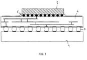
- Figure 1 shows an integrated circuit 2 which is "flip-chip” bonded to a substrate 4 by means of metallized contacts 6 of solder referred to in the art as "bumps".
- the substrate 4 can be a printed circuit board or an intermediate package such as a Ball Grid Array (BGA) or Chip-Scale-Package (CSP) itself bonded to a printed circuit board 9 through additional solder balls 7 or leads.
- the package can be formed of organic, ceramic, or metal materials.
- the present invention utilizes metal solders which are substantially lead-free (aside from lead present at an impurity level, typically 10p.p.m being tolerated). It is found that particularly advantageous compositions include pure tin, or tin which includes a small amount of an alloying element such as copper, silver, or bismuth, or both silver and copper. It is found that the incorporation of such an alloying element is effective in lowering the melting point of pure tin, in preventing the formation of whiskers on as-plated deposits, in lowering the surface tension of tin (550 dyne/cm at 232°C), to improve the mechanical properties of tin (such as ductility), and in preventing a phase change of pure tin from 8 to form which occurs below 13°C. This phase change is accompanied by a volume change which leads to a decrease in mechanical strength, as well as compromising bond integrity and strength.
- the solder bump materials are discussed in further detail below.
- Figures 2(a) to (d) and 3(a)/(al) to (d) illustrate a fabrication process for forming metal solder bump interconnections of the described compositions utilizing an electroplating technique.
- Figure 2(a) shows the semiconductor wafer 8 to which has previously been applied at appropriate locations bond pads, which are conventionally made of Al:Si (1-2wt%Si) or Al:Si:Cu (1-2wt%Si and 1-5wt%Cu), or more recently pure copper, and a glass passivation layer 12 which extends over the wafer, but is removed at appropriate positions to expose the bond pads 10.
- the bond pads make electrical connection to the active areas of the chips.
- the first step involves cleaning of the wafer 8 by a backsputter process performed under vacuum in order to remove the naturally formed oxide layer on the bond pads.
- the cleaning step is followed by the sputter deposition of a single or series of metal layers 14 and usually two as indicated in Fig. 2(b).
- the first metal layer which is typically made of chrome, with a thickness of between 500 - 1000 ⁇ performs a number of functions including increasing adhesion to the cleaned bond pads, and to the glass passivation, preventing re-oxidation of the metal pad and forming a barrier diffusion layer to the solder. Ti/W, NiV or Ti may also be used for the first layer.
- the second metal layer is formed of copper of thickness 2500-10000 ⁇ to form a seed layer for the under bump metal and to also provide a contact plating (electrical buss) layer. Nikel may be used in lieu of copper for the second layer.
- the next step consists of patterning the wafer with a thick (preferably between 50 - 200 ⁇ m) layer of an ultra-violet sensitive photoimagable organic film 16 such as a liquid photoresist or dry film as indicated in Fig. 2(c) which is deposited by spinning it onto the surface of the wafer following by baking to harden the layer, or by lamination of the dry film.
- a two-step application and baking may be required.
- the photosensitive layer is then patterned by exposing it through a metal-coated glass photomask which has openings selectively etched in the metal layer to define the areas to be bumped. These openings allow ultra-violet light to pass through and expose the photosensitive layer.
- the thickness of the photosensitive layer and the size of the opening determines in part the final volume and shape of the solder bump.
- the thickness is important to ensure sufficient bump height is obtained to ensure sufficient chip stand-off from the substrate after the bump is reflowed and flip-chip bonded.
- Either positive or negative tone photosensitive polymers may be used for this process.
- electrical contacts points are opened at the edges of the wafer to the underlying sputtered copper layer and the wafer is then plated with either copper (or nickel) to form the under-bump-metal (UBM) 18 as indicated in Fig. 2(d).
- UBM under-bump-metal
- the wafer is then electroplated with solder (Fig. 3(a)) and by selecting the appropriate type of plating solution and anodes in the plating bath, lead-free deposits of pure tin, or alloys comprising tin-copper, tin-silver, or tin-bismuth bumps 20 can be formed from a single plating solution with simultaneous co-deposition of the respective elements in the desired stoichiometry.
- Plating solutions from a variety of providers can be employed, for example those of Shipley Ronal. For pure tin electroplating Shipley Ronal's "Tinglo Culmo" product is particularly appropriate, whilst for tin-bismuth their "Solderon BI" product is appropriate.
- a negative voltage is usually applied to the wafer effectively making it the cathode.
- a pure tin anode or tin-copper anode is utilized in the case of a soluble anode technique, or for tin-bismuth deposition an insoluble platinized titanium anode is preferred.
- the tin-copper, tin-bismuth, and tin-silver plated deposits can be formed either from a single plating solution with simultaneous co-deposition of the respective elements in the desired stoichiometric amounts or by sequential plating of the pure elements (in the desired amounts) followed by reflow of the plated deposit to achieve an alloy with the desired composition.
- An applied current density of 3-5 A.S.D (amps per square decimetre) is found to be appropriate.
- Either direct current (DC) or pulse-plating techniques can be used in conjunction with rack or fountain (cup) plating equipment.
- 3-5V with a current of between 0.05 to 0.1A is preferred.
- a pulsed alternating current a pulse comprising about +5V for about 1 millisecond, followed by zero V for about 1 millisecond, followed by -5V for 1 millisecond, followed by zero V for 1 millisecond is found to be beneficial in terms of bump uniformity and composition of the deposit.
- the pure elements may be deposited by sequentially plating from separate plating solutions, and controlling the plating time to control the relative amounts of each element. Whilst this results in a layered structure of the pure elements, when the plated deposit is reflowed (as discussed further below) the resultant bump is an alloy of the desired stoichiometry.
- This sequential plating can be employed for any of the binary alloys discussed. It is found to be generally unimportant which element is plated first and which second.
- tin-silver-copper this sequential technique is found to be particularly useful, as plating of ternary alloys from a single plating solution is difficult owing to the difficulty in accurately controlling the resultant alloy composition.
- a tin-copper deposit is preferably formed separately from the silver by first simultaneously co-depositing tin-copper from a single binary plating solution, followed by plating of pure silver. On reflow of the as-plated deposits the desired ternary alloy is formed.
- the silver may be deposited first, followed by plating of tin-copper.
- the three individual elements may be sequentially deposited. This option is viable for deposition of relatively large bumps, but becomes more difficult with smaller bumps owing to the fact that the proportion of copper is small (less than 2%, and preferably about 0.7%), and accurate control of the amount of deposited copper becomes then more difficult.
- the bump will form a pillar shape (Fig. 3(a1). If the plating process is continued above the height of the photoresist, a "mushroom” shape will form (Fig. 3(a)). Mushrooming can be used if necessary to increase the volume of the solder in instances where it is not possible to pattern the photosensitive layer to the desired height.
- Flux is then applied to the as-plated bumps and they are re-flowed in an oven to form the spherical solder shape 20'.
- a flux-less reflow of the bump can be achieved when using a combination of a reducing nitrogen and hydrogen environment.
- bump solder materials are as follows:
- Figure 4(a) is a scanning electron micrograph of eutectic tin-copper bumps as-plated, whilst Figure 4(b) shows these after reflow, showing highly regular well-defined bumps.
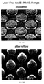
- Figures 5(a) and (b) are scanning electron micrographs of tin-bismuth solder bumps for 90wt%Sn:10wt%Bi, also exhibiting regular well-defined solder bumps of appropriate height for bonding to a substrate.
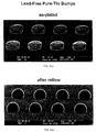
- Figures 6(a) and (b) are scanning electron micrographs of as-plated and after reflow pure tin solder bumps.
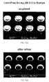
- Figures 7(a) and (b) are scanning electron micrographs of the as-plated and after reflow tin-silver solder bumps for 96.5wt%Sn:3.5wt%Ag showing regular well-defined solder bumps.
- Figures 8(a) and (b) are scanning electron micrographs of the as-plated and after reflow tin-silver-copper solder bumps for 95.7wt%Sn:3.5wt%Ag:0.8%Cu fabricated using the method of sequential plating of tin-silver followed by tin-copper.
Landscapes
- Engineering & Computer Science (AREA)
- Mechanical Engineering (AREA)
- Chemical & Material Sciences (AREA)
- Chemical Kinetics & Catalysis (AREA)
- Electrochemistry (AREA)
- Materials Engineering (AREA)
- Metallurgy (AREA)
- Organic Chemistry (AREA)
- Wire Bonding (AREA)
- Electroplating Methods And Accessories (AREA)
Abstract
Description
- The present invention relates to a method of forming lead-free solder bump interconnections on semiconductor wafers for flip-chip bonding applications.
- With flip-chip interconnect technology, a raised electrically conductive contact called a "bump" is first formed onto the input/output connection pads of an integrated circuit (IC) which is subsequently assembled face-down (or "flip-chip" bonded) without the use of conventional wire bonds or leads. Various bump interconnection media have been proposed including gold, lead-tin solder, nickel, copper, and conductive polymers. Lead-tin bumps are particularly attractive due to the self-alignment and self-planarizing properties (upon reflow) of solder which allows for a more robust and manufacturable attachment process. In addition to providing electrical contact, the solder bump also forms a mechanical, and thermal connection between the chip and substrate. The use of lead-tin solder bumps for flip-chip applications was first introduced by IBM in the 1960's in their C4 (controlled-collapse-chip-connection) technology using a method of evaporation for fabrication of the bumps.
- Primary advantages of flip-chip technology as compared to other interconnection techniques include:
- i) the capacity to significantly increase the total number of connections that can be made to the chip because the small bump contacts can be placed virtually anywhere on the surface of the chip and at points convenient for a particular application (unlike "perimeter-only" bonding technologies such as wire-bonding and tape-automated-bonding (TAB));
- ii) the potential to shrink the die size and obviate the need for long metallization lines leading to the periphery pads which would favourably impact both the IC manufacturing yield and reliability;
- iii) lower electrical resistance and inductance values leading to faster interconnection speeds and lower power consumption;
- iv) better thermal dissipation performance due to conduction through the solder bumps and exposed rear surface of the IC after flip-chip bonding;
- v) provision for a smaller, lighter, and more compact package with overall lower packaging cost per pin.
-
- The selection of the precise composition of a solder bump material is conventionally influenced by a variety of factors, most particularly melting point. Attention must be paid to the solder melting point, particularly where the chip is bonded to a substrate which are mostly formed of low-cost organic materials with relatively low Tg (glass transition temperatures). When the IC is flip-chip bonded, it is normally heated to a temperature which is typically 20-30°C higher than the melting point of the solder. Too high a melting point for the solder bump may therefore lead to damage of the substrate.
- The two most common bump materials currently in use for flip-chip bonding applications consist of pure gold and lead-tin based alloys. The former are used mainly to flip-chip a silicon IC onto liquid crystal displays (LCDs) or in TAB packages. Lead-tin solder bumps are used primarily for flip-chip-on-board or flip-chip-in-package applications.
Solder bumps are typically preferred over gold bumps due to their lower cost and self-planarizing and self-aligning reflow characteristics which provides for a more manufacturable and robust flip-chip bonding process. - Lead-tin alloys commonly employed as solder bumps include in particular 95wt%Pb/5wt%Sn, 97wt%Pb/3wt%Sn, and eutectic 37wt%Pb/63wt%Sn. Lead-based solders with additions of In, Ag, and Bi have also been proposed.
- With growing environmental awareness, a worldwide ban on the use of lead-containing solders in electronic products is under consideration since the lead from such products, which are typically disposed of in landfills, eventually leaches into the drinking water system. Laws restricting the use of lead in electronics products may be enacted in the European Community, and similar legislation to ban lead is pending in the United States and in Japan. Efforts to identify suitable lead-free finishes for electronic components has thus far been focused mainly on printed circuit boards, leadframe packages, and in the selection of solder pastes. Little attention has been paid to the fabrication of bump interconnections for flip-chip applications.
- Lead-free solders have been proposed including those based on indium and its alloys with bismuth, tin, antimony, zinc and silver.
- What is required are lead-free solder bump compositions which can be directly substituted for the lead-tin alloys conventionally used for flip-chip applications, and a fabrication method employing such a lead-free solder bump composition.
- It is proposed in US Patent No. 5410184 assigned to Motorola to utilise a lead-free solder alloy having tin as a predominant component, between 2-8%wt or more preferably 3-5%wt copper and up to 1.5%wt silver. This solder requires the presence of an amount of copper at preferably 3-5%wt so as to retain formation of a certain degree of intermetallics for bond integrity. It is found however that this composition may suffer problems of bond embrittlement owing to an excessive formation of the tin-copper intermetallics.
- The present invention seeks to provide a process for forming solder bumps which overcomes the problems mentioned above.
- According to a first aspect the invention resides in a method of forming solder bumps on a chip or wafer for flip-chip applications, comprising the steps of providing a chip or wafer having a plurality of metal bonds pads which provide electrical connection to the chip or wafer, and applying a solder bump comprising pure tin or a tin alloy selected from tin-copper, tin-silver, tin-bismuth or tin-silver-copper by an electroplating technique, and melting the solder bumps by heating to a temperature above the bump melting point to effect reflow.
- The solder is more preferably one of pure tin, tin-copper alloy of less than 2% weight copper or more preferably about 0.7% by weight copper, tin-silver alloy having less than 20% by weight silver or more preferably about 3.5% by weight silver, or 10% by weight silver, tin-bismuth having between 5% and 25% by weight bismuth or more preferably about 20% by weight bismuth, or tin-silver-copper alloy having less than 5wt% silver, and preferably about 3.5wt%Ag, less than 2wt% copper and preferably about 0.7wt%Cu, with the balance being tin.
- It is found that pure tin or the tin alloys can be directly substituted for the conventional lead-tin alloys, whilst the solder bumps can be formed using electroplating to give particularly well-defined, regular bumps. The tin-based solders identified are also compatible with existing reflow processes and materials, and with surface mount techniques and equipment.
- In the case of the binary alloys tin-copper, tin-silver and tin-bismuth the elements can be simultaneously co-deposited as the alloy from a single plating solution.
- In an alternative technique the elements can be sequentially deposited from separate plating solutions, which form the requisite alloys on heating during the reflow process. This sequential plating is particularly applicable also to the ternary alloy tin-silver-copper. In this case the alloy is deposited by depositing one or other of tin-copper alloy from a single plating solution by co-deposition, or elemental silver, followed by deposition of the other, the ternary alloy forming on heating. It is also possible to sequentially deposit each of the three elements.
- The chip or wafer may be, before electroplating, provided with a sputtered layer or layers of metal which function as a diffusion barrier, barrier to oxidation, adhesion, and plating contact layer (electrical buss). A layer of thick photosensitive polymer material such as photoresist (negative or positive tone) or dry film with a thickness of between 25 - 200 µm is used to define the location and volume of the solder bumps to be plated. The provision of thick photoresist or dry-film is important to ensure sufficient height and volume of the plated solder bump without causing shorting to the next adjacent bump, and to maintain the necessary stand-off height between the chip and the substrate in order to compensate for differences in thermal coefficients of expansion of the chip and the substrate as well to provide a sufficient gap for underfill material to flow between the chip and the substrate after flip-chip bonding.
- The electroplating of the solder bumps can be carried out using either direct current (DC) or pulsed alternating current. The current and voltage values depend on the size of the wafer and the total exposed surface area to be plated. Preferable DC plating parameters range between 3-5 V with a current of between 0.05-0.1 A. In a preferable pulsed plating cycle voltage alternates between +5 V for about 1 millisecond, a zero voltage portion for about 1 millisecond or less, between -5 to -10 V for 1 millisecond, followed by zero voltage for about 1 millisecond.
- Either rack or fountain plating equipment may be used for plating of the solder on the wafers.
- According to a further aspect the invention resides in a method for forming solder bumps on a chip or wafer for flip-chip applications comprising the steps of: (a) providing a chip or wafer having a passivation layer and a plurality of exposed metallic bond pads; (b) applying at least one solder-wettable metal layer to the bond pad; (c) applying a photosensitive layer to the chip or wafer having openings at the portions of the bond pads; (d) applying a solder comprising pure tin, or a tin alloy selected from tin-copper, tin-silver, tin-bismuth, or tin-silver-copper by an electroplating technique; (e) removing the photoresist layer; and (f) melting the solder bumps to effect reflow.
- The invention also resides in a chip or wafer when formed according to the methods described above.
- Embodiments of the invention are now described, by way of example only, with reference to the following drawings in which:
- Figure 1 is a sectional view of a flip-chip in a package;
- Figures 2(a) to (d) illustrate the first four stages of deposition of solder bumps;
- Figures 3(a) to (d) illustrate the deposition steps subsequent to those of Figures 2(a) to (d);
- Figures 4(a) and (b) show scanning electron micrographs of tin-copper bumps formed according to the invention; Figures 5 (a) and (b) show scanning electron micrographs of tin-bismuth bumps formed according to the invention; Figures 6(a) and (b) show scanning electron micrographs of pure tin bumps;
- Figure 7(a) and (b) shows scanning electron micrographs of tin-silver bumps according to the invention; and
- Figures 8(a) and (b) show scanning electron micrographs of tin-silver-copper bumps according to the invention.
-
- Turning to the drawings, Figure 1 shows an
integrated circuit 2 which is "flip-chip" bonded to a substrate 4 by means of metallized contacts 6 of solder referred to in the art as "bumps". The substrate 4 can be a printed circuit board or an intermediate package such as a Ball Grid Array (BGA) or Chip-Scale-Package (CSP) itself bonded to a printed circuit board 9 throughadditional solder balls 7 or leads. The package can be formed of organic, ceramic, or metal materials. - The present invention utilizes metal solders which are substantially lead-free (aside from lead present at an impurity level, typically 10p.p.m being tolerated). It is found that particularly advantageous compositions include pure tin, or tin which includes a small amount of an alloying element such as copper, silver, or bismuth, or both silver and copper. It is found that the incorporation of such an alloying element is effective in lowering the melting point of pure tin, in preventing the formation of whiskers on as-plated deposits, in lowering the surface tension of tin (550 dyne/cm at 232°C), to improve the mechanical properties of tin (such as ductility), and in preventing a phase change of pure tin from 8 to form which occurs below 13°C. This phase change is accompanied by a volume change which leads to a decrease in mechanical strength, as well as compromising bond integrity and strength. The solder bump materials are discussed in further detail below.
- Figures 2(a) to (d) and 3(a)/(al) to (d) illustrate a fabrication process for forming metal solder bump interconnections of the described compositions utilizing an electroplating technique.
- Figure 2(a) shows the
semiconductor wafer 8 to which has previously been applied at appropriate locations bond pads, which are conventionally made of Al:Si (1-2wt%Si) or Al:Si:Cu (1-2wt%Si and 1-5wt%Cu), or more recently pure copper, and aglass passivation layer 12 which extends over the wafer, but is removed at appropriate positions to expose thebond pads 10. The bond pads make electrical connection to the active areas of the chips. - The first step involves cleaning of the
wafer 8 by a backsputter process performed under vacuum in order to remove the naturally formed oxide layer on the bond pads. The cleaning step is followed by the sputter deposition of a single or series ofmetal layers 14 and usually two as indicated in Fig. 2(b). The first metal layer which is typically made of chrome, with a thickness of between 500 - 1000 Å performs a number of functions including increasing adhesion to the cleaned bond pads, and to the glass passivation, preventing re-oxidation of the metal pad and forming a barrier diffusion layer to the solder. Ti/W, NiV or Ti may also be used for the first layer. The second metal layer is formed of copper of thickness 2500-10000Å to form a seed layer for the under bump metal and to also provide a contact plating (electrical buss) layer. Nikel may be used in lieu of copper for the second layer. - The next step consists of patterning the wafer with a thick (preferably between 50 - 200 µm) layer of an ultra-violet sensitive photoimagable
organic film 16 such as a liquid photoresist or dry film as indicated in Fig. 2(c) which is deposited by spinning it onto the surface of the wafer following by baking to harden the layer, or by lamination of the dry film. To produce such a thickness with liquid resists, a two-step application and baking may be required. The photosensitive layer is then patterned by exposing it through a metal-coated glass photomask which has openings selectively etched in the metal layer to define the areas to be bumped. These openings allow ultra-violet light to pass through and expose the photosensitive layer. The thickness of the photosensitive layer and the size of the opening determines in part the final volume and shape of the solder bump. The thickness is important to ensure sufficient bump height is obtained to ensure sufficient chip stand-off from the substrate after the bump is reflowed and flip-chip bonded. Either positive or negative tone photosensitive polymers may be used for this process. After developing the photosensitive layer, which provides a protective layer to areas that are not to be plated, electrical contacts points are opened at the edges of the wafer to the underlying sputtered copper layer and the wafer is then plated with either copper (or nickel) to form the under-bump-metal (UBM) 18 as indicated in Fig. 2(d). This layer which is normally between 3-7 µm thick acts as a "wettable" foundation to the solder bump. - The wafer is then electroplated with solder (Fig. 3(a)) and by selecting the appropriate type of plating solution and anodes in the plating bath, lead-free deposits of pure tin, or alloys comprising tin-copper, tin-silver, or tin-
bismuth bumps 20 can be formed from a single plating solution with simultaneous co-deposition of the respective elements in the desired stoichiometry. Plating solutions from a variety of providers can be employed, for example those of Shipley Ronal. For pure tin electroplating Shipley Ronal's "Tinglo Culmo" product is particularly appropriate, whilst for tin-bismuth their "Solderon BI" product is appropriate. A negative voltage is usually applied to the wafer effectively making it the cathode. For each of these desired alloys either a pure tin anode or tin-copper anode is utilized in the case of a soluble anode technique, or for tin-bismuth deposition an insoluble platinized titanium anode is preferred. The tin-copper, tin-bismuth, and tin-silver plated deposits can be formed either from a single plating solution with simultaneous co-deposition of the respective elements in the desired stoichiometric amounts or by sequential plating of the pure elements (in the desired amounts) followed by reflow of the plated deposit to achieve an alloy with the desired composition. An applied current density of 3-5 A.S.D (amps per square decimetre) is found to be appropriate. Either direct current (DC) or pulse-plating techniques can be used in conjunction with rack or fountain (cup) plating equipment. For D.C. plating 3-5V with a current of between 0.05 to 0.1A is preferred. For a pulsed alternating current, a pulse comprising about +5V for about 1 millisecond, followed by zero V for about 1 millisecond, followed by -5V for 1 millisecond, followed by zero V for 1 millisecond is found to be beneficial in terms of bump uniformity and composition of the deposit. - It has also been found that instead of simultaneously depositing the respective elements from a single plating solution, the pure elements may be deposited by sequentially plating from separate plating solutions, and controlling the plating time to control the relative amounts of each element. Whilst this results in a layered structure of the pure elements, when the plated deposit is reflowed (as discussed further below) the resultant bump is an alloy of the desired stoichiometry. This sequential plating can be employed for any of the binary alloys discussed. It is found to be generally unimportant which element is plated first and which second.
- In the case of tin-silver-copper this sequential technique is found to be particularly useful, as plating of ternary alloys from a single plating solution is difficult owing to the difficulty in accurately controlling the resultant alloy composition. In this case a tin-copper deposit is preferably formed separately from the silver by first simultaneously co-depositing tin-copper from a single binary plating solution, followed by plating of pure silver. On reflow of the as-plated deposits the desired ternary alloy is formed. Alternatively, the silver may be deposited first, followed by plating of tin-copper. As a further alternative, the three individual elements may be sequentially deposited. This option is viable for deposition of relatively large bumps, but becomes more difficult with smaller bumps owing to the fact that the proportion of copper is small (less than 2%, and preferably about 0.7%), and accurate control of the amount of deposited copper becomes then more difficult.
- If the plating process is stopped before the solder reaches the top of the patterned photosensitive layer, the bump will form a pillar shape (Fig. 3(a1). If the plating process is continued above the height of the photoresist, a "mushroom" shape will form (Fig. 3(a)). Mushrooming can be used if necessary to increase the volume of the solder in instances where it is not possible to pattern the photosensitive layer to the desired height.
- Further steps in completing the bump fabrication process involve removal of the protective photosensitive layer as shown in Fig. 3(b) and back-etching of the sputtered copper and chrome layers using chemical means as indicated in Fig. 3(c).
- Flux is then applied to the as-plated bumps and they are re-flowed in an oven to form the spherical solder shape 20'. Alternatively a flux-less reflow of the bump can be achieved when using a combination of a reducing nitrogen and hydrogen environment.
- The particular selected bump solder materials are as follows:
- a) Pure Tin This is selected because it is the simplest, cheapest, and easiest to fabricate as a lead-free replacement for lead-tin bumps, and yet has fairly similar physical, electrical and thermal characteristics to lead-tin solder. It also has a low toxicity and good solderability.Despite the fact that there is a strong prejudice against using pure tin in microelectronic packages due to the well-documented effect of formation over time of tin whiskers (which can cause shorting and device failure), the use as solder bump for a flip-chip application does not suffer the problem of whisker formation. It is believed that whisker formation is a stress-time dependent effect, and it is believed the reflow process relieves this stress.
- b) Tin-Copper The percentage of copper must be less than 2wt% and preferably in the region of about 0.7wt% which represents the eutectic point, this composition exhibiting a melting point of 227°C. Concentrations of copper much greater than about 2% are undesirable as they have an increased melting point (which increases fabrication problems) and because copper forms intermetallic compounds with tin which are brittle and therefore mechanically unstable. The tin-copper alloy system with a composition of 99.3wt%Sn/0.7wt%Cu with a melting point of 227°C can be considered as a lead-free replacement for high-lead (95wt%Pb/5wt%Sn or 97wt%Pb/3wt%Sn) alloys which have melting points in excess of 300°C. The tin-copper alloy systems could also be considered as a replacement for eutectic lead-tin bumps if the substrate is able to tolerate a reflow temperature of about 260°C.
- c) Tin-Silver The percentage of silver for most applications must be less than 5%wt and preferably 3.5%wt which is the eutectic point of the alloy system. Small additions of silver may be desired since they have shown to significantly increase the ductility of pure tin which may be desirable in cases where the bumps may be subjected to stress and multiple thermal cycling. Concentrations of silver higher than 3.5%wt are typically not desirable due to the high cost of silver. Moreover, the melting point of the Sn-Ag system increases rapidly with increasing silver content. For example, at the eutectic point of 3.5%wt silver the melting point is 221°C. At 10%wt silver the melting point is 300°C which is too high for most low-cost organic substrate or packaging materials. However, in cases where a high melting point (in excess of 300°C) lead-free solder bump is desired, such as for flip-chip bonding onto ceramic substrates, a silver composition of less than 20% and more preferably about 10% is preferred. At 20% silver the melting point is about 375°C which is potentially useful for certain high temperature applications, although at 10% silver the melting point is about 300°C which is comparable to the melting point of existing 95wt%Pb/5wt%Sn and 95wt%Pb/3wt%Sn alloys. Thus, the eutectic (96.5wt%Sn/3.5wt%Ag) and high-silver (90wt%Sn/10wt%Ag) content alloys can be considered as lead-free replacements of eutectic (37wt%Pb/63wt%Sn) and high-lead (95wt%Pb/5wt%Sn or 97wt%Pb/3wt%Sn) alloys respectively.
- d) Tin-Bismuth The percentage of bismuth is selected to be in the range of 10-25%wt. The tin-bismuth system exhibits an acceptable melting point over a wide range of compositions; 225°C at 10% Bi and 138.5°C at 60% (which represents the eutectic point). At about 20%wt bismuth, the melting point of the Sn-Bi alloy is 185°C which is similar to that of eutectic lead-tin at 183°C so this particular Sn-Bi alloy can therefore be used as a "drop-in" replacement to the eutectic lead-tin solder.
- e) Tin-Silver-Copper The tin-silver-copper alloy has a composition of less than 5wt% silver, preferably in the region of 3.5wt%Ag, less than 2wt% copper, preferably in the region of 0.7wt%Cu, with the balance being tin. This alloy has a melting point of between 216°C and 217°C which makes it suitable as a substitute for eutectic lead-tin solders.
-
- The above-described elemental tin and tin alloy compositions applied by electroplating are found to produce solder bumps which are lead free whilst having properties compatible with those of conventional lead-tin solder bumps.
- Figure 4(a) is a scanning electron micrograph of eutectic tin-copper bumps as-plated, whilst Figure 4(b) shows these after reflow, showing highly regular well-defined bumps.
- Figures 5(a) and (b) are scanning electron micrographs of tin-bismuth solder bumps for 90wt%Sn:10wt%Bi, also exhibiting regular well-defined solder bumps of appropriate height for bonding to a substrate.
- Figures 6(a) and (b) are scanning electron micrographs of as-plated and after reflow pure tin solder bumps.
- Figures 7(a) and (b) are scanning electron micrographs of the as-plated and after reflow tin-silver solder bumps for 96.5wt%Sn:3.5wt%Ag showing regular well-defined solder bumps.
- Figures 8(a) and (b) are scanning electron micrographs of the as-plated and after reflow tin-silver-copper solder bumps for 95.7wt%Sn:3.5wt%Ag:0.8%Cu fabricated using the method of sequential plating of tin-silver followed by tin-copper.
Claims (21)
- A method of forming solder bumps on a chip or wafer for flip-chip applications, comprising the steps of providing a chip or wafer having a plurality of metal bonds pads which provide electrical connection to the chip or wafer, and applying a solder bump comprising pure tin or a tin alloy selected from tin-copper, tin-silver, tin-bismuth, or tin-silver-copper by an electroplating technique, and melting the solder bumps by heating to a temperature above the bump melting point to effect reflow.
- A method according to claim 1 wherein the solder is tin-copper alloy having less than 2% by weight copper, the balance being tin.
- A method according to claim 2 wherein the solder is tin-copper alloy having about 0.7% by weight copper.
- A method according to claim 1 wherein the solder is tin-silver alloy having less than 20% by weight silver, the balance being tin.
- A method according to claim 4 wherein the tin-silver alloy has about 3.5% by weight silver, the balance being tin.
- A method according to claim 4 wherein the tin-silver alloy has about 10% by weight silver, the balance being tin.
- A method according to claim 1 wherein the solder is tin-bismuth having between 5 and 25% by weight bismuth, the balance being tin.
- A method according to claim 7 having about 20% by weight bismuth, the balance being tin.
- A method according to claim 1 wherein the solder is tin-silver-copper alloy having less than 5wt% silver and less than 2wt% copper, the balance being tin.
- A method according to claim 9 having about 3.5wt% silver.
- A method according to claim 9 having about 0.7wt% copper.
- A method according to claim 1 wherein the elements of the tin-copper, tin-silver or tin-bismuth alloys are simultaneously co-deposited as the alloy from a single plating solution.
- A method according to claim 1 wherein the tin-copper, tin-silver, tin-bismuth or tin-silver-copper alloys are deposited by sequentially plating pure elements, which form the requisite alloys on heating.
- A method according to claim 1 wherein the tin-silver copper alloy is deposited by depositing one or other of tin-copper alloy from a single plating solution by co-deposition, or elemental silver, followed by deposition of the other, the ternary alloy forming on heating.
- A method according to claim 1 wherein the chip or wafer is provided with a layer of thick photosensitive material patterned to define the location of the solder bumps, the photosensitive material being of between 25 and 200 µm thickness.
- A method according to claim 1 wherein the electroplating is carried out using a direct current.
- A method according to claim 1 wherein the electroplating is carried out using a pulsed alternating current.
- A method according to claim 17 wherein each pulse comprises about +5V for about 1 millisecond, zero voltage for about 1 millisecond, about -5V for about 1 millisecond, followed by zero voltage for about 1 millisecond.
- A method for forming solder bumps on a chip or wafer for flip-chip applications comprising the steps of:(a) providing a chip or wafer having a passivation layer and a plurality of exposed metallic bond pads;(b) applying at least one solder-wettable metal layer to the bond pad;(c) applying a photosensitive layer to the chip or wafer having openings at the portions of the bond pads;(d) applying a solder comprising pure tin, or a tin alloy selected from tin-copper, tin-silver, tin-bismuth or tin-silver-copper by an electroplating technique;(e) removing the photosensitive layer; and(f) melting the solder bumps to effect reflow.
- A chip or wafer having solder bumps formed according to the method of claim 1.
- A chip or wafer having solder bumps formed according to the method of claim 19.
Applications Claiming Priority (2)
| Application Number | Priority Date | Filing Date | Title |
|---|---|---|---|
| US09/552,560 US6638847B1 (en) | 2000-04-19 | 2000-04-19 | Method of forming lead-free bump interconnections |
| US552560 | 2000-04-19 |
Publications (2)
| Publication Number | Publication Date |
|---|---|
| EP1148548A2 true EP1148548A2 (en) | 2001-10-24 |
| EP1148548A3 EP1148548A3 (en) | 2002-01-30 |
Family
ID=24205862
Family Applications (1)
| Application Number | Title | Priority Date | Filing Date |
|---|---|---|---|
| EP01302292A Ceased EP1148548A3 (en) | 2000-04-19 | 2001-03-13 | Method of forming lead-free bump interconnections |
Country Status (8)
| Country | Link |
|---|---|
| US (1) | US6638847B1 (en) |
| EP (1) | EP1148548A3 (en) |
| JP (1) | JP3748785B2 (en) |
| KR (1) | KR20010098699A (en) |
| CN (1) | CN100416784C (en) |
| GB (1) | GB2361450B (en) |
| HK (1) | HK1043245B (en) |
| SG (1) | SG94808A1 (en) |
Cited By (22)
| Publication number | Priority date | Publication date | Assignee | Title |
|---|---|---|---|---|
| DE10123280A1 (en) * | 2001-05-14 | 2002-12-05 | Infineon Technologies Ag | Production of contact bumps used in the production of flip-chip assemblies comprises applying copper to a support element, applying tin to the copper, and heating the copper and tin to a temperature at which remelting occurs |
| EP1353228A1 (en) | 2002-04-11 | 2003-10-15 | Shipley Co. L.L.C. | Method for depositing a very thick photoresist layer on a substrate and metal plating method |
| DE10237495A1 (en) * | 2002-04-22 | 2003-11-13 | Siemens Ag | Solder material used in the production of electrical/electronic components using Flip-Chip technology contains aluminum |
| EP1410871A1 (en) * | 2002-10-17 | 2004-04-21 | Senju Metal Industry Co., Ltd. | Lead-free solder ball |
| WO2004034460A3 (en) * | 2002-10-09 | 2004-06-03 | Motorola Inc | Method for eliminating voiding in plated solder |
| WO2003077319A3 (en) * | 2002-03-13 | 2004-06-03 | Oy Ajat Ltd | Low temperature, bump-bonded radiation imaging device |
| US6790758B2 (en) * | 2002-11-25 | 2004-09-14 | Silicon Integrated Systems Corp. | Method for fabricating conductive bumps and substrate with metal bumps for flip chip packaging |
| WO2005031848A1 (en) * | 2003-09-22 | 2005-04-07 | Intel Corporation | Designs and methods for conductive bumps |
| DE10355953A1 (en) * | 2003-11-29 | 2005-07-07 | Infineon Technologies Ag | Method of electroplating and contact projection arrangement |
| WO2006004809A1 (en) * | 2004-06-30 | 2006-01-12 | Unitive International Limited | Methods of forming lead free solder bumps and related structures |
| US7081372B2 (en) * | 2003-07-09 | 2006-07-25 | Chartered Semiconductor Manufacturing Ltd. | Aluminum cap with electroless nickel/immersion gold |
| EP1598448A4 (en) * | 2002-12-26 | 2007-03-07 | Ebara Corp | LEAD-FREE BOSS AND METHOD FOR FORMING THE SAME |
| US7259095B2 (en) | 2002-04-26 | 2007-08-21 | Nec Electronics Corporation | Semiconductor device and manufacturing process therefor as well as plating solution |
| DE102006051491A1 (en) * | 2006-10-31 | 2008-05-15 | Advanced Micro Devices, Inc., Sunnyvale | Metallization layer stack with an aluminum termination metal layer |
| EP1970762A1 (en) | 2007-03-12 | 2008-09-17 | Rohm and Haas Electronic Materials, L.L.C. | Phenolic polymers and photoresists comprising same |
| DE102008020924A1 (en) * | 2008-04-25 | 2009-11-05 | Siemens Aktiengesellschaft | Electrical and/or mechanical connections manufacturing method for gamma or X-ray detectors, involves producing elevation as seed layer, metallic column and solder layer based on substrate or electronic element |
| US7879715B2 (en) | 2002-06-25 | 2011-02-01 | Unitive International Limited | Methods of forming electronic structures including conductive shunt layers and related structures |
| EP2336828A2 (en) | 2009-12-15 | 2011-06-22 | Rohm and Haas Electronic Materials LLC | Photoresists and methods for use thereof |
| EP2336829A1 (en) | 2009-12-15 | 2011-06-22 | Rohm and Haas Electronic Materials LLC | Photoresists and methods for use thereof |
| EP2336827A1 (en) | 2009-12-15 | 2011-06-22 | Rohm and Haas Electronic Materials LLC | Photoresists and methods for use thereof |
| EP2472327A1 (en) | 2010-12-30 | 2012-07-04 | Rohm and Haas Electronic Materials LLC | Photoresists and methods for use thereof |
| ES2418279R1 (en) * | 2011-10-10 | 2013-10-30 | Sala Genaro Barange | WELDING WITHOUT THE USE OF THE HEADPHONE TERMINALS LEAD |
Families Citing this family (100)
| Publication number | Priority date | Publication date | Assignee | Title |
|---|---|---|---|---|
| US6863209B2 (en) | 2000-12-15 | 2005-03-08 | Unitivie International Limited | Low temperature methods of bonding components |
| JP3813497B2 (en) * | 2001-11-12 | 2006-08-23 | 株式会社ルネサステクノロジ | Bump forming method and semiconductor device mounting structure |
| TWI245402B (en) | 2002-01-07 | 2005-12-11 | Megic Corp | Rod soldering structure and manufacturing process thereof |
| TW521361B (en) * | 2002-02-27 | 2003-02-21 | Advanced Semiconductor Eng | Bump process |
| JP2003303842A (en) * | 2002-04-12 | 2003-10-24 | Nec Electronics Corp | Semiconductor device and method of manufacturing the same |
| JP3888210B2 (en) * | 2002-04-17 | 2007-02-28 | 凸版印刷株式会社 | Film carrier manufacturing method |
| US6596621B1 (en) * | 2002-05-17 | 2003-07-22 | International Business Machines Corporation | Method of forming a lead-free tin-silver-copper based solder alloy on an electronic substrate |
| US7531898B2 (en) | 2002-06-25 | 2009-05-12 | Unitive International Limited | Non-Circular via holes for bumping pads and related structures |
| US7547623B2 (en) | 2002-06-25 | 2009-06-16 | Unitive International Limited | Methods of forming lead free solder bumps |
| TWI281718B (en) * | 2002-09-10 | 2007-05-21 | Advanced Semiconductor Eng | Bump and process thereof |
| US6892925B2 (en) * | 2002-09-18 | 2005-05-17 | International Business Machines Corporation | Solder hierarchy for lead free solder joint |
| US6854636B2 (en) * | 2002-12-06 | 2005-02-15 | International Business Machines Corporation | Structure and method for lead free solder electronic package interconnections |
| JP2004207685A (en) * | 2002-12-23 | 2004-07-22 | Samsung Electronics Co Ltd | Manufacturing method of lead-free solder bump |
| TW571411B (en) * | 2002-12-25 | 2004-01-11 | Advanced Semiconductor Eng | Bumping process |
| JP2004204308A (en) * | 2002-12-25 | 2004-07-22 | Nec Semiconductors Kyushu Ltd | Lead-free tin alloy plating method |
| US7015590B2 (en) | 2003-01-10 | 2006-03-21 | Samsung Electronics Co., Ltd. | Reinforced solder bump structure and method for forming a reinforced solder bump |
| US6959856B2 (en) | 2003-01-10 | 2005-11-01 | Samsung Electronics Co., Ltd. | Solder bump structure and method for forming a solder bump |
| US20040155097A1 (en) * | 2003-02-04 | 2004-08-12 | Matsushita Electric Industrial Co., Ltd. | Soldering method and method for manufacturing component mounting board |
| TWI225899B (en) | 2003-02-18 | 2005-01-01 | Unitive Semiconductor Taiwan C | Etching solution and method for manufacturing conductive bump using the etching solution to selectively remove barrier layer |
| TW591780B (en) * | 2003-03-21 | 2004-06-11 | Univ Nat Central | Flip chip Au bump structure and method of manufacturing the same |
| US6917113B2 (en) * | 2003-04-24 | 2005-07-12 | International Business Machines Corporatiion | Lead-free alloys for column/ball grid arrays, organic interposers and passive component assembly |
| US20050026416A1 (en) * | 2003-07-31 | 2005-02-03 | International Business Machines Corporation | Encapsulated pin structure for improved reliability of wafer |
| TWI242866B (en) * | 2003-08-21 | 2005-11-01 | Siliconware Precision Industries Co Ltd | Process of forming lead-free bumps on electronic component |
| JP2005085857A (en) * | 2003-09-05 | 2005-03-31 | Denso Corp | Electrode structure using bumps |
| KR101025844B1 (en) * | 2003-10-01 | 2011-03-30 | 삼성전자주식회사 | SnAgAb solder bumps, a method of manufacturing the same and a light emitting device bonding method using the method |
| CN1319129C (en) * | 2003-11-28 | 2007-05-30 | 悠立半导体股份有限公司 | Solder bump formation method |
| KR100698662B1 (en) * | 2003-12-02 | 2007-03-23 | 에프씨엠 가부시끼가이샤 | Terminals forming surfaces consisting of tin-silver-copper ternary alloys, parts and articles |
| US7410833B2 (en) * | 2004-03-31 | 2008-08-12 | International Business Machines Corporation | Interconnections for flip-chip using lead-free solders and having reaction barrier layers |
| TW200603698A (en) | 2004-04-13 | 2006-01-16 | Unitive International Ltd | Methods of forming solder bumps on exposed metal pads and related structures |
| US20050275096A1 (en) * | 2004-06-11 | 2005-12-15 | Kejun Zeng | Pre-doped reflow interconnections for copper pads |
| US7179738B2 (en) * | 2004-06-17 | 2007-02-20 | Texas Instruments Incorporated | Semiconductor assembly having substrate with electroplated contact pads |
| US7494041B2 (en) * | 2004-06-23 | 2009-02-24 | Intel Corporation | In-situ alloyed solders, articles made thereby, and processes of making same |
| US20060043603A1 (en) * | 2004-08-31 | 2006-03-02 | Lsi Logic Corporation | Low temperature PB-free processing for semiconductor devices |
| CN100336215C (en) * | 2004-09-30 | 2007-09-05 | 江阴长电先进封装有限公司 | Micron level chip packing structure |
| TWI242253B (en) * | 2004-10-22 | 2005-10-21 | Advanced Semiconductor Eng | Bumping process and structure thereof |
| US7411303B2 (en) * | 2004-11-09 | 2008-08-12 | Texas Instruments Incorporated | Semiconductor assembly having substrate with electroplated contact pads |
| CN100424842C (en) * | 2004-11-17 | 2008-10-08 | 日本特殊陶业株式会社 | Manufacturing method of wiring board |
| US7371676B2 (en) | 2005-04-08 | 2008-05-13 | Micron Technology, Inc. | Method for fabricating semiconductor components with through wire interconnects |
| GB0507887D0 (en) * | 2005-04-20 | 2005-05-25 | Rohm & Haas Elect Mat | Immersion method |
| US7393770B2 (en) | 2005-05-19 | 2008-07-01 | Micron Technology, Inc. | Backside method for fabricating semiconductor components with conductive interconnects |
| US7713859B2 (en) | 2005-08-15 | 2010-05-11 | Enthone Inc. | Tin-silver solder bumping in electronics manufacture |
| CN1933106B (en) * | 2005-09-12 | 2010-04-28 | 中芯国际集成电路制造(上海)有限公司 | Method for manufacturing gold bumps with smoother surface |
| JP4890835B2 (en) * | 2005-10-28 | 2012-03-07 | ルネサスエレクトロニクス株式会社 | Manufacturing method of semiconductor device |
| US7307348B2 (en) | 2005-12-07 | 2007-12-11 | Micron Technology, Inc. | Semiconductor components having through wire interconnects (TWI) |
| KR100719905B1 (en) | 2005-12-29 | 2007-05-18 | 삼성전자주식회사 | Sn-based solder alloys and semiconductor devices using the same |
| KR100843632B1 (en) * | 2006-01-04 | 2008-07-03 | 한양대학교 산학협력단 | Flip chip mount type of bump, manufacturing method thereof, and bonding method for flip chip using non conductive adhesive |
| KR100722645B1 (en) * | 2006-01-23 | 2007-05-28 | 삼성전기주식회사 | Printed circuit board for semiconductor package and manufacturing method |
| TW200731430A (en) * | 2006-02-08 | 2007-08-16 | Jung-Tang Huang | Controllable method for manufacturing uniform planarity of plating-based solder bumps on multi-layer flip chip used in the three-dimensional packaging |
| US7684205B2 (en) * | 2006-02-22 | 2010-03-23 | General Dynamics Advanced Information Systems, Inc. | System and method of using a compliant lead interposer |
| US7659612B2 (en) | 2006-04-24 | 2010-02-09 | Micron Technology, Inc. | Semiconductor components having encapsulated through wire interconnects (TWI) |
| JP5162851B2 (en) * | 2006-07-14 | 2013-03-13 | 富士通セミコンダクター株式会社 | Semiconductor device and manufacturing method thereof |
| JP4354469B2 (en) * | 2006-08-11 | 2009-10-28 | シャープ株式会社 | Semiconductor device and manufacturing method of semiconductor device |
| DE102007021009A1 (en) * | 2006-09-27 | 2008-04-10 | Osram Opto Semiconductors Gmbh | Light-emitting diode arrangement and method for producing such |
| US8404160B2 (en) | 2007-05-18 | 2013-03-26 | Applied Nanotech Holdings, Inc. | Metallic ink |
| US10231344B2 (en) | 2007-05-18 | 2019-03-12 | Applied Nanotech Holdings, Inc. | Metallic ink |
| JP4708399B2 (en) * | 2007-06-21 | 2011-06-22 | 新光電気工業株式会社 | Electronic device manufacturing method and electronic device |
| US20090008764A1 (en) * | 2007-07-02 | 2009-01-08 | Hsin-Hui Lee | Ultra-Thin Wafer-Level Contact Grid Array |
| KR100871067B1 (en) * | 2007-07-13 | 2008-11-27 | 성균관대학교산학협력단 | High strength solder bump manufacturing method by forming copper post |
| KR100894869B1 (en) * | 2007-09-27 | 2009-04-24 | 한국생산기술연구원 | Ternary lead-free solder fine bumps using binary alloy plating containing nanoparticles and its formation method |
| SG152101A1 (en) * | 2007-11-06 | 2009-05-29 | Agency Science Tech & Res | An interconnect structure and a method of fabricating the same |
| US7847399B2 (en) * | 2007-12-07 | 2010-12-07 | Texas Instruments Incorporated | Semiconductor device having solder-free gold bump contacts for stability in repeated temperature cycles |
| US7807572B2 (en) * | 2008-01-04 | 2010-10-05 | Freescale Semiconductor, Inc. | Micropad formation for a semiconductor |
| JP4724192B2 (en) * | 2008-02-28 | 2011-07-13 | 株式会社東芝 | Manufacturing method of electronic parts |
| US8506849B2 (en) | 2008-03-05 | 2013-08-13 | Applied Nanotech Holdings, Inc. | Additives and modifiers for solvent- and water-based metallic conductive inks |
| US8197612B2 (en) * | 2008-04-29 | 2012-06-12 | International Business Machines Corporation | Optimization of metallurgical properties of a solder joint |
| KR101025418B1 (en) * | 2008-05-09 | 2011-03-28 | 앰코 테크놀로지 코리아 주식회사 | Semiconductor device and manufacturing method thereof |
| US9730333B2 (en) | 2008-05-15 | 2017-08-08 | Applied Nanotech Holdings, Inc. | Photo-curing process for metallic inks |
| US8143158B2 (en) * | 2008-09-29 | 2012-03-27 | Intel Corporation | Method and device of preventing delamination of semiconductor layers |
| CN101740420B (en) * | 2008-11-05 | 2011-11-09 | 中芯国际集成电路制造(上海)有限公司 | Process for manufacturing copper strut |
| US7915741B2 (en) * | 2009-02-24 | 2011-03-29 | Unisem Advanced Technologies Sdn. Bhd. | Solder bump UBM structure |
| JP5740389B2 (en) | 2009-03-27 | 2015-06-24 | アプライド・ナノテック・ホールディングス・インコーポレーテッド | Buffer layer to enhance photosintering and / or laser sintering |
| CN101908516B (en) * | 2009-06-04 | 2011-12-28 | 中芯国际集成电路制造(上海)有限公司 | Tin-silver convex block structure of flip chip and manufacturing method thereof |
| US8422197B2 (en) | 2009-07-15 | 2013-04-16 | Applied Nanotech Holdings, Inc. | Applying optical energy to nanoparticles to produce a specified nanostructure |
| CN102005396B (en) * | 2009-08-28 | 2012-12-05 | 中芯国际集成电路制造(上海)有限公司 | Bump making method and bump structure |
| JP2011165862A (en) * | 2010-02-09 | 2011-08-25 | Sony Corp | Semiconductor device, chip-on-chip mounting structure, method for manufacturing semiconductor device, and method for forming chip-on-chip mounting structure |
| KR101125603B1 (en) * | 2010-02-23 | 2012-03-27 | 한국과학기술연구원 | Manufacturing method of microelectrode array |
| KR20110124993A (en) * | 2010-05-12 | 2011-11-18 | 삼성전자주식회사 | Semiconductor chip, semiconductor package and method for manufacturing same |
| US8759872B2 (en) | 2010-06-22 | 2014-06-24 | Suvolta, Inc. | Transistor with threshold voltage set notch and method of fabrication thereof |
| EP2405469B1 (en) * | 2010-07-05 | 2016-09-21 | ATOTECH Deutschland GmbH | Method to form solder alloy deposits on substrates |
| CN102339767A (en) * | 2010-07-26 | 2012-02-01 | 矽品精密工业股份有限公司 | Semiconductor device and method for manufacturing the same |
| US8410604B2 (en) | 2010-10-26 | 2013-04-02 | Xilinx, Inc. | Lead-free structures in a semiconductor device |
| US20120325671A2 (en) * | 2010-12-17 | 2012-12-27 | Tel Nexx, Inc. | Electroplated lead-free bump deposition |
| JP5659821B2 (en) * | 2011-01-26 | 2015-01-28 | 三菱マテリアル株式会社 | Manufacturing method of Sn alloy bump |
| US8496159B2 (en) | 2011-06-06 | 2013-07-30 | International Business Machines Corporation | Injection molded solder process for forming solder bumps on substrates |
| JP6054612B2 (en) * | 2012-03-06 | 2016-12-27 | ラピスセミコンダクタ株式会社 | Semiconductor integrated device |
| KR101932727B1 (en) | 2012-05-07 | 2018-12-27 | 삼성전자주식회사 | Bump structure, semiconductor package having the bump structure, and method of manufacturing the bump structure |
| TW201419315A (en) | 2012-07-09 | 2014-05-16 | Applied Nanotech Holdings Inc | Photosintering of micron-sized copper particles |
| KR101574135B1 (en) * | 2013-10-10 | 2015-12-03 | (주)포인트엔지니어링 | Method for mounting a chip and chip package |
| CN103887276B (en) * | 2014-04-04 | 2016-06-01 | 华进半导体封装先导技术研发中心有限公司 | Prevent bump structure and the forming method of convex some side direction etching |
| US10062657B2 (en) | 2014-10-10 | 2018-08-28 | Ishihara Chemical Co., Ltd. | Method for manufacturing alloy bump |
| US9546433B1 (en) | 2015-11-24 | 2017-01-17 | International Business Machines Corporation | Separation of alpha emitting species from plating baths |
| US9425164B1 (en) | 2015-11-24 | 2016-08-23 | International Business Machines Corporation | Low alpha tin |
| US9359687B1 (en) | 2015-11-24 | 2016-06-07 | International Business Machines Corporation | Separation of alpha emitting species from plating baths |
| CN106112162B (en) * | 2016-07-25 | 2018-04-17 | 江苏科技大学 | A kind of method for being used to reduce the formation of tin bismuth solder joint intermetallic compound |
| KR102198850B1 (en) | 2018-11-29 | 2021-01-05 | 덕산하이메탈(주) | Low melting solder alloy and solder ball manufactured by using the same |
| JP7336258B2 (en) * | 2019-05-15 | 2023-08-31 | イビデン株式会社 | Printed wiring board and manufacturing method thereof |
| JP7378247B2 (en) * | 2019-09-05 | 2023-11-13 | イビデン株式会社 | Printed wiring board and its manufacturing method |
| CN114121868A (en) * | 2020-08-28 | 2022-03-01 | 京东方科技集团股份有限公司 | Substrate and manufacturing method thereof, display device and manufacturing method thereof |
| CN112045329B (en) * | 2020-09-07 | 2022-03-11 | 中国电子科技集团公司第二十四研究所 | A flip-chip soldering process method for ball-planting on a metal substrate |
| CN114645243A (en) * | 2022-03-04 | 2022-06-21 | 微智医疗器械有限公司 | Processing method of bonding pad of electronic element, circuit board assembly and electronic equipment |
Citations (2)
| Publication number | Priority date | Publication date | Assignee | Title |
|---|---|---|---|---|
| US5410184A (en) * | 1993-10-04 | 1995-04-25 | Motorola | Microelectronic package comprising tin-copper solder bump interconnections, and method for forming same |
| EP0831683A1 (en) * | 1996-09-19 | 1998-03-25 | Nortel Networks Corporation | Assemblies of substrates and electronic components |
Family Cites Families (22)
| Publication number | Priority date | Publication date | Assignee | Title |
|---|---|---|---|---|
| US4159231A (en) * | 1978-08-04 | 1979-06-26 | The United States Of America As Represented By The Secretary Of The Interior | Method of producing a lead dioxide coated cathode |
| US4721551A (en) * | 1986-11-06 | 1988-01-26 | The Regents Of The University Of California | Iridium treatment of neuro-stimulating electrodes |
| US4922322A (en) | 1989-02-09 | 1990-05-01 | National Semiconductor Corporation | Bump structure for reflow bonding of IC devices |
| US5039576A (en) | 1989-05-22 | 1991-08-13 | Atochem North America, Inc. | Electrodeposited eutectic tin-bismuth alloy on a conductive substrate |
| US5229016A (en) * | 1991-08-08 | 1993-07-20 | Microfab Technologies, Inc. | Method and apparatus for dispensing spherical-shaped quantities of liquid solder |
| US5316205A (en) | 1993-04-05 | 1994-05-31 | Motorola, Inc. | Method for forming gold bump connection using tin-bismuth solder |
| US5818699A (en) | 1995-07-05 | 1998-10-06 | Kabushiki Kaisha Toshiba | Multi-chip module and production method thereof |
| US6224690B1 (en) * | 1995-12-22 | 2001-05-01 | International Business Machines Corporation | Flip-Chip interconnections using lead-free solders |
| KR100268967B1 (en) | 1996-01-30 | 2000-10-16 | 모기 준이치 | Method for producing a plating product using an aqueous solution for forming a metal complex, a tin-silver alloy plating bath and the plating bath |
| US5851482A (en) | 1996-03-22 | 1998-12-22 | Korea Institute Of Machinery & Metals | Tin-bismuth based lead-free solder for copper and copper alloys |
| US5949654A (en) | 1996-07-03 | 1999-09-07 | Kabushiki Kaisha Toshiba | Multi-chip module, an electronic device, and production method thereof |
| US5873161A (en) * | 1996-07-23 | 1999-02-23 | Minnesota Mining And Manufacturing Company | Method of making a Z axis interconnect circuit |
| US5750017A (en) | 1996-08-21 | 1998-05-12 | Lucent Technologies Inc. | Tin electroplating process |
| US6179935B1 (en) | 1997-04-16 | 2001-01-30 | Fuji Electric Co., Ltd. | Solder alloys |
| US6117299A (en) | 1997-05-09 | 2000-09-12 | Mcnc | Methods of electroplating solder bumps of uniform height on integrated circuit substrates |
| AU7592198A (en) | 1997-05-23 | 1998-12-11 | Alpine Microsystems, Inc. | A system and method for packaging integrated circuits |
| KR100219806B1 (en) | 1997-05-27 | 1999-09-01 | 윤종용 | Method for manufacturing flip chip mounted solder bumps of semiconductor device, solder bumps manufactured accordingly, and analysis method thereof |
| JP3592486B2 (en) * | 1997-06-18 | 2004-11-24 | 株式会社東芝 | Soldering equipment |
| JP3296289B2 (en) * | 1997-07-16 | 2002-06-24 | 富士電機株式会社 | Solder alloy |
| US5937320A (en) | 1998-04-08 | 1999-08-10 | International Business Machines Corporation | Barrier layers for electroplated SnPb eutectic solder joints |
| JP2000054189A (en) | 1998-08-10 | 2000-02-22 | Furukawa Electric Co Ltd:The | Electric / electronic component material used by bonding Sn-Bi solder, electric / electronic component using the same, electric / electronic component mounting board, and solder bonding or mounting method using the same |
| JP2000068410A (en) | 1998-08-20 | 2000-03-03 | Nishihara Riko Kk | IC package such as BGA or CSP with bump terminals plated with bonding material instead of Pb |
-
2000
- 2000-04-19 US US09/552,560 patent/US6638847B1/en not_active Expired - Fee Related
- 2000-12-18 GB GB0030870A patent/GB2361450B/en not_active Expired - Fee Related
-
2001
- 2001-03-13 EP EP01302292A patent/EP1148548A3/en not_active Ceased
- 2001-03-30 JP JP2001100474A patent/JP3748785B2/en not_active Expired - Fee Related
- 2001-04-18 SG SG200102265A patent/SG94808A1/en unknown
- 2001-04-18 KR KR1020010020765A patent/KR20010098699A/en not_active Ceased
- 2001-04-19 CN CNB011153210A patent/CN100416784C/en not_active Expired - Fee Related
-
2002
- 2002-04-19 HK HK02102993.1A patent/HK1043245B/en not_active IP Right Cessation
Patent Citations (2)
| Publication number | Priority date | Publication date | Assignee | Title |
|---|---|---|---|---|
| US5410184A (en) * | 1993-10-04 | 1995-04-25 | Motorola | Microelectronic package comprising tin-copper solder bump interconnections, and method for forming same |
| EP0831683A1 (en) * | 1996-09-19 | 1998-03-25 | Nortel Networks Corporation | Assemblies of substrates and electronic components |
Cited By (33)
| Publication number | Priority date | Publication date | Assignee | Title |
|---|---|---|---|---|
| DE10123280A1 (en) * | 2001-05-14 | 2002-12-05 | Infineon Technologies Ag | Production of contact bumps used in the production of flip-chip assemblies comprises applying copper to a support element, applying tin to the copper, and heating the copper and tin to a temperature at which remelting occurs |
| WO2003077319A3 (en) * | 2002-03-13 | 2004-06-03 | Oy Ajat Ltd | Low temperature, bump-bonded radiation imaging device |
| EP1353228A1 (en) | 2002-04-11 | 2003-10-15 | Shipley Co. L.L.C. | Method for depositing a very thick photoresist layer on a substrate and metal plating method |
| US7344970B2 (en) | 2002-04-11 | 2008-03-18 | Shipley Company, L.L.C. | Plating method |
| SG145567A1 (en) * | 2002-04-11 | 2008-09-29 | Shipley Co Llc | Plating method |
| DE10237495A1 (en) * | 2002-04-22 | 2003-11-13 | Siemens Ag | Solder material used in the production of electrical/electronic components using Flip-Chip technology contains aluminum |
| US7821135B2 (en) | 2002-04-26 | 2010-10-26 | Nec Electronics Corporation | Semiconductor device with improved stress migration resistance and manufacturing process therefor |
| US7259095B2 (en) | 2002-04-26 | 2007-08-21 | Nec Electronics Corporation | Semiconductor device and manufacturing process therefor as well as plating solution |
| DE10318921B4 (en) * | 2002-04-26 | 2015-02-19 | Renesas Electronics Corporation | Manufacturing method for a semiconductor device |
| US8294269B2 (en) | 2002-06-25 | 2012-10-23 | Unitive International | Electronic structures including conductive layers comprising copper and having a thickness of at least 0.5 micrometers |
| US7879715B2 (en) | 2002-06-25 | 2011-02-01 | Unitive International Limited | Methods of forming electronic structures including conductive shunt layers and related structures |
| WO2004034460A3 (en) * | 2002-10-09 | 2004-06-03 | Motorola Inc | Method for eliminating voiding in plated solder |
| EP1410871A1 (en) * | 2002-10-17 | 2004-04-21 | Senju Metal Industry Co., Ltd. | Lead-free solder ball |
| US6790758B2 (en) * | 2002-11-25 | 2004-09-14 | Silicon Integrated Systems Corp. | Method for fabricating conductive bumps and substrate with metal bumps for flip chip packaging |
| EP1598448A4 (en) * | 2002-12-26 | 2007-03-07 | Ebara Corp | LEAD-FREE BOSS AND METHOD FOR FORMING THE SAME |
| US7081372B2 (en) * | 2003-07-09 | 2006-07-25 | Chartered Semiconductor Manufacturing Ltd. | Aluminum cap with electroless nickel/immersion gold |
| US7276801B2 (en) | 2003-09-22 | 2007-10-02 | Intel Corporation | Designs and methods for conductive bumps |
| US11201129B2 (en) | 2003-09-22 | 2021-12-14 | Intel Corporation | Designs and methods for conductive bumps |
| US10249588B2 (en) | 2003-09-22 | 2019-04-02 | Intel Corporation | Designs and methods for conductive bumps |
| US9543261B2 (en) | 2003-09-22 | 2017-01-10 | Intel Corporation | Designs and methods for conductive bumps |
| WO2005031848A1 (en) * | 2003-09-22 | 2005-04-07 | Intel Corporation | Designs and methods for conductive bumps |
| US8580679B2 (en) | 2003-09-22 | 2013-11-12 | Intel Corporation | Designs and methods for conductive bumps |
| DE10355953B4 (en) * | 2003-11-29 | 2005-10-20 | Infineon Technologies Ag | Method of electroplating and contact projection arrangement |
| DE10355953A1 (en) * | 2003-11-29 | 2005-07-07 | Infineon Technologies Ag | Method of electroplating and contact projection arrangement |
| WO2006004809A1 (en) * | 2004-06-30 | 2006-01-12 | Unitive International Limited | Methods of forming lead free solder bumps and related structures |
| DE102006051491A1 (en) * | 2006-10-31 | 2008-05-15 | Advanced Micro Devices, Inc., Sunnyvale | Metallization layer stack with an aluminum termination metal layer |
| EP1970762A1 (en) | 2007-03-12 | 2008-09-17 | Rohm and Haas Electronic Materials, L.L.C. | Phenolic polymers and photoresists comprising same |
| DE102008020924A1 (en) * | 2008-04-25 | 2009-11-05 | Siemens Aktiengesellschaft | Electrical and/or mechanical connections manufacturing method for gamma or X-ray detectors, involves producing elevation as seed layer, metallic column and solder layer based on substrate or electronic element |
| EP2336827A1 (en) | 2009-12-15 | 2011-06-22 | Rohm and Haas Electronic Materials LLC | Photoresists and methods for use thereof |
| EP2336829A1 (en) | 2009-12-15 | 2011-06-22 | Rohm and Haas Electronic Materials LLC | Photoresists and methods for use thereof |
| EP2336828A2 (en) | 2009-12-15 | 2011-06-22 | Rohm and Haas Electronic Materials LLC | Photoresists and methods for use thereof |
| EP2472327A1 (en) | 2010-12-30 | 2012-07-04 | Rohm and Haas Electronic Materials LLC | Photoresists and methods for use thereof |
| ES2418279R1 (en) * | 2011-10-10 | 2013-10-30 | Sala Genaro Barange | WELDING WITHOUT THE USE OF THE HEADPHONE TERMINALS LEAD |
Also Published As
| Publication number | Publication date |
|---|---|
| CN100416784C (en) | 2008-09-03 |
| GB2361450A (en) | 2001-10-24 |
| HK1043245B (en) | 2003-04-11 |
| EP1148548A3 (en) | 2002-01-30 |
| GB0030870D0 (en) | 2001-01-31 |
| HK1043245A1 (en) | 2002-09-06 |
| JP3748785B2 (en) | 2006-02-22 |
| KR20010098699A (en) | 2001-11-08 |
| US6638847B1 (en) | 2003-10-28 |
| SG94808A1 (en) | 2003-03-18 |
| GB2361450B (en) | 2002-06-26 |
| CN1320960A (en) | 2001-11-07 |
| JP2001308129A (en) | 2001-11-02 |
Similar Documents
| Publication | Publication Date | Title |
|---|---|---|
| US6638847B1 (en) | Method of forming lead-free bump interconnections | |
| US8026613B2 (en) | Interconnections for flip-chip using lead-free solders and having reaction barrier layers | |
| US7932169B2 (en) | Interconnection for flip-chip using lead-free solders and having improved reaction barrier layers | |
| KR100334593B1 (en) | Semiconductor device and method of the same | |
| US6224690B1 (en) | Flip-Chip interconnections using lead-free solders | |
| US8497200B2 (en) | Method to form solder alloy deposits on substrates | |
| US11121101B2 (en) | Flip chip packaging rework | |
| US20020086520A1 (en) | Semiconductor device having bump electrode | |
| US20150290746A1 (en) | Composition of a solder, and method of manufacturing a solder connection | |
| US6716738B2 (en) | Method of fabricating multilayered UBM for flip chip interconnections by electroplating | |
| US20050017376A1 (en) | IC chip with improved pillar bumps | |
| JP2004207685A (en) | Manufacturing method of lead-free solder bump | |
| WO2007097508A1 (en) | Semiconductor chip with solder bump suppressing growth of inter-metallic compound and method of frabricating the same | |
| WO2006004809A1 (en) | Methods of forming lead free solder bumps and related structures | |
| US20090020871A1 (en) | Semiconductor chip with solder bump suppressing growth of inter-metallic compound and method of fabricating the same | |
| Arshad et al. | Under bump metallurgy (UBM)-A technology review for flip chip packaging | |
| KR100534108B1 (en) | Method of fabricating Pb-free solder bumps | |
| US20090266480A1 (en) | Process for Preparing a Solder Stand-Off | |
| Karim et al. | Lead-free solder bump technologies for flip-chip packaging applications | |
| TW502424B (en) | Method of forming lead-free bump interconnections | |
| JP2001352005A (en) | Wiring board and semiconductor device |
Legal Events
| Date | Code | Title | Description |
|---|---|---|---|
| PUAI | Public reference made under article 153(3) epc to a published international application that has entered the european phase |
Free format text: ORIGINAL CODE: 0009012 |
|
| AK | Designated contracting states |
Kind code of ref document: A2 Designated state(s): AT BE CH CY DE DK ES FI FR GB GR IE IT LI LU MC NL PT SE TR |
|
| AX | Request for extension of the european patent |
Free format text: AL;LT;LV;MK;RO;SI |
|
| PUAL | Search report despatched |
Free format text: ORIGINAL CODE: 0009013 |
|
| AK | Designated contracting states |
Kind code of ref document: A3 Designated state(s): AT BE CH CY DE DK ES FI FR GB GR IE IT LI LU MC NL PT SE TR |
|
| AX | Request for extension of the european patent |
Free format text: AL;LT;LV;MK;RO;SI |
|
| 17P | Request for examination filed |
Effective date: 20020709 |
|
| AKX | Designation fees paid |
Free format text: AT BE CH CY DE DK ES FI FR GB GR IE IT LI LU MC NL PT SE TR |
|
| 17Q | First examination report despatched |
Effective date: 20030725 |
|
| STAA | Information on the status of an ep patent application or granted ep patent |
Free format text: STATUS: THE APPLICATION HAS BEEN REFUSED |
|
| 18R | Application refused |
Effective date: 20070717 |