EP1136852A9 - Selecteur de mode de diffraction de guides d'ondes en reseau - Google Patents
Selecteur de mode de diffraction de guides d'ondes en reseau Download PDFInfo
- Publication number
- EP1136852A9 EP1136852A9 EP00951897A EP00951897A EP1136852A9 EP 1136852 A9 EP1136852 A9 EP 1136852A9 EP 00951897 A EP00951897 A EP 00951897A EP 00951897 A EP00951897 A EP 00951897A EP 1136852 A9 EP1136852 A9 EP 1136852A9
- Authority
- EP
- European Patent Office
- Prior art keywords
- waveguides
- arrayed
- core
- refractive index
- waveguide grating
- Prior art date
- Legal status (The legal status is an assumption and is not a legal conclusion. Google has not performed a legal analysis and makes no representation as to the accuracy of the status listed.)
- Withdrawn
Links
- 230000003287 optical effect Effects 0.000 claims abstract description 45
- 238000009826 distribution Methods 0.000 claims abstract description 31
- 230000008021 deposition Effects 0.000 claims abstract description 12
- 238000006460 hydrolysis reaction Methods 0.000 claims abstract description 10
- 230000007062 hydrolysis Effects 0.000 claims abstract description 9
- 230000000644 propagated effect Effects 0.000 claims description 11
- 239000000203 mixture Substances 0.000 abstract description 13
- 238000005253 cladding Methods 0.000 abstract description 8
- 239000000758 substrate Substances 0.000 abstract description 5
- XUIMIQQOPSSXEZ-UHFFFAOYSA-N Silicon Chemical compound [Si] XUIMIQQOPSSXEZ-UHFFFAOYSA-N 0.000 abstract description 4
- 229910052710 silicon Inorganic materials 0.000 abstract description 4
- 239000010703 silicon Substances 0.000 abstract description 4
- 241001505295 Eros Species 0.000 abstract 1
- 239000010410 layer Substances 0.000 description 45
- 230000005540 biological transmission Effects 0.000 description 29
- 238000000411 transmission spectrum Methods 0.000 description 19
- 238000000151 deposition Methods 0.000 description 17
- 239000012792 core layer Substances 0.000 description 13
- 238000000034 method Methods 0.000 description 5
- 239000011521 glass Substances 0.000 description 4
- 239000000463 material Substances 0.000 description 4
- 239000002245 particle Substances 0.000 description 4
- 238000004519 manufacturing process Methods 0.000 description 3
- 239000013307 optical fiber Substances 0.000 description 3
- 230000002194 synthesizing effect Effects 0.000 description 3
- 238000009833 condensation Methods 0.000 description 2
- 230000005494 condensation Effects 0.000 description 2
- 230000006866 deterioration Effects 0.000 description 2
- 230000000694 effects Effects 0.000 description 2
- 230000005684 electric field Effects 0.000 description 2
- 238000005259 measurement Methods 0.000 description 2
- 238000000206 photolithography Methods 0.000 description 2
- 238000001020 plasma etching Methods 0.000 description 2
- 230000003595 spectral effect Effects 0.000 description 2
- 238000002834 transmittance Methods 0.000 description 2
- 230000002542 deteriorative effect Effects 0.000 description 1
- 238000009472 formulation Methods 0.000 description 1
- YBMRDBCBODYGJE-UHFFFAOYSA-N germanium oxide Inorganic materials O=[Ge]=O YBMRDBCBODYGJE-UHFFFAOYSA-N 0.000 description 1
- 238000002955 isolation Methods 0.000 description 1
- 239000010453 quartz Substances 0.000 description 1
- VYPSYNLAJGMNEJ-UHFFFAOYSA-N silicon dioxide Inorganic materials O=[Si]=O VYPSYNLAJGMNEJ-UHFFFAOYSA-N 0.000 description 1
- 239000004071 soot Substances 0.000 description 1
Images


Classifications
-
- G—PHYSICS
- G02—OPTICS
- G02B—OPTICAL ELEMENTS, SYSTEMS OR APPARATUS
- G02B6/00—Light guides; Structural details of arrangements comprising light guides and other optical elements, e.g. couplings
- G02B6/10—Light guides; Structural details of arrangements comprising light guides and other optical elements, e.g. couplings of the optical waveguide type
- G02B6/12—Light guides; Structural details of arrangements comprising light guides and other optical elements, e.g. couplings of the optical waveguide type of the integrated circuit kind
- G02B6/12007—Light guides; Structural details of arrangements comprising light guides and other optical elements, e.g. couplings of the optical waveguide type of the integrated circuit kind forming wavelength selective elements, e.g. multiplexer, demultiplexer
- G02B6/12009—Light guides; Structural details of arrangements comprising light guides and other optical elements, e.g. couplings of the optical waveguide type of the integrated circuit kind forming wavelength selective elements, e.g. multiplexer, demultiplexer comprising arrayed waveguide grating [AWG] devices, i.e. with a phased array of waveguides
- G02B6/12011—Light guides; Structural details of arrangements comprising light guides and other optical elements, e.g. couplings of the optical waveguide type of the integrated circuit kind forming wavelength selective elements, e.g. multiplexer, demultiplexer comprising arrayed waveguide grating [AWG] devices, i.e. with a phased array of waveguides characterised by the arrayed waveguides, e.g. comprising a filled groove in the array section
-
- G—PHYSICS
- G02—OPTICS
- G02B—OPTICAL ELEMENTS, SYSTEMS OR APPARATUS
- G02B6/00—Light guides; Structural details of arrangements comprising light guides and other optical elements, e.g. couplings
- G02B6/10—Light guides; Structural details of arrangements comprising light guides and other optical elements, e.g. couplings of the optical waveguide type
- G02B6/12—Light guides; Structural details of arrangements comprising light guides and other optical elements, e.g. couplings of the optical waveguide type of the integrated circuit kind
- G02B6/13—Integrated optical circuits characterised by the manufacturing method
- G02B6/132—Integrated optical circuits characterised by the manufacturing method by deposition of thin films
-
- G—PHYSICS
- G02—OPTICS
- G02B—OPTICAL ELEMENTS, SYSTEMS OR APPARATUS
- G02B6/00—Light guides; Structural details of arrangements comprising light guides and other optical elements, e.g. couplings
- G02B6/10—Light guides; Structural details of arrangements comprising light guides and other optical elements, e.g. couplings of the optical waveguide type
- G02B6/12—Light guides; Structural details of arrangements comprising light guides and other optical elements, e.g. couplings of the optical waveguide type of the integrated circuit kind
- G02B6/13—Integrated optical circuits characterised by the manufacturing method
- G02B6/136—Integrated optical circuits characterised by the manufacturing method by etching
Definitions
- the present invention relates to an arrayed waveguide grating to be used in the field of optical transmissions.
- an arrayed waveguide grating As an example of an optical transmission element for optical wavelength division multiplexing transmissions, there is an arrayed waveguide grating (AWG) as shown in Fig. 9.
- the arrayed waveguide grating is formed so that waveguide forming part 10 having a waveguide composition as shown in the same figure is provided on substrate 11.
- the composition of the waveguide is as follows.
- first slab waveguide 13 is connected to the exit side of one or more optical input waveguides 12 which are disposed in parallel.
- a plurality of arrayed waveguides 14 disposed in parallel are connected to the exit side of the first slab waveguide 13, and second slab waveguide 15 is connected to the exit sides of the plurality of arrayed waveguides 14.
- a plurality of optical output waveguides 16 disposed in parallel are connected to the exit side of the second slab waveguide 15.
- the arrayed waveguides 14 propagate light led out from the first slab waveguide 13, and are formed so as to have lengths which are different from each other.
- the optical input waveguides 12 and optical output waveguides 14 are provided so as to accord to the number of, for example, signal light beams which have varying wavelengths to be demultiplexed by the arrayed waveguide grating.
- the arrayed waveguides 16 are provided by a large number, for example, 100. However, in this figure, for simplification of the figure, the number of the waveguides 12, 14, and 16 are simplified.
- An optical fiber at the transmission side is connected to the optical input waveguides 12, whereby wavelength multiplexed light is led therein.
- Light which has passed through the optical input waveguides 12 and has been led into the first slab waveguide 13 is spread by the diffraction effect, made incident onto the plurality of arrayed waveguides 14, and propagated in the arrayed waveguides 14.
- Light propagated in the arrayed waveguides 14 reaches the second slab waveguide 15, and furthermore, is condensed by the optical output waveguides 16 and outputted. Since the lengths of the arrayed waveguides 14 are different from each other, phase differences occur in the light beams after being propagated in the arrayed waveguides 14. In accordance with the phase differences, the wavefront of the converged light inclines, and in accordance with the angle of this inclination, the light condensation position is determined. Therefore, the condensation positions of the light beams with varying wavelengths are different from each other, and output waveguides 16 are formed at these positions, whereby light beams with varying wavelengths can be outputted from the different optical output waveguides 16 for each wavelength.
- wavelength multiplexed light beams with wavelengths of ⁇ 1, ⁇ 2, ⁇ 3,... ⁇ n are inputted from one optical input waveguide 12, these light beams are expanded in the first slab waveguide 13. Then, the light beams reach the arrayed waveguides 14, pass through the second slab waveguide 15, and as mentioned above, are condensed on different positions at the exit end of the second slab waveguide 15 for each wavelength. Thereafter, the light beams which are different in wavelength from each other are made incident onto different optical output waveguides 16, pass through the respective optical output waveguides 16, and are outputted from the exit ends of the optical output waveguides 16. When an optical fiber for outputting light is connected to the exit ends of the optical output waveguides 16, the light beams with varying wavelengths are taken out via this optical fiber.
- the wavelength resolution of the grating is in proportion to the differences ( ⁇ L) in length between the arrayed waveguides 14 which comprise the grating. Therefore, by properly setting the ⁇ L, wavelength multiplexed light can be demultiplexed at narrow wavelength intervals.
- an arrayed waveguide grating is proposed which is arranged so that the difference in optical path lengths between the arrayed waveguides 14 is set to 65.2 ⁇ m, the order of diffraction is set to 61, the total number of arrayed waveguides 14 is set to 100, and wavelength multiplexed light is demultiplexed into 32 waves at intervals of 100GHz.
- an arrayed waveguide grating When manufacturing an arrayed waveguide grating, first, flame hydrolysis deposition is used to deposit and form a lower cladding layer on silicon substrate 11, and then the layer is consolidate. Next, flame hydrolysis deposition is used to deposit and form a core layer on the consolidate lower cladding layer, and then the core layer is consolidate. Thereafter, an arrayed waveguide grating pattern is transferred onto the core layer by means of photolithography and the reactive ion etching method via a photomask on which the arrayed waveguide grating is drawn.
- the core is etched, and the waveguide composition (waveguide pattern) of the arrayed waveguide grating is formed.
- an upper cladding layer is formed by means of flame hydrolysis deposition and consolidate, whereby the arrayed waveguide grating is formed.
- the number of deposited layers of the core is generally 6.
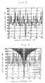
- Fig. 10 an example of the transmission spectrum of the arrayed waveguide grating is shown.
- the arrayed waveguide grating having this transmission spectrum is manufactured so that the number of deposited layers of the core is 6, and the optical path length difference between the arrayed waveguides 14, the total number of the waveguides, and the order of diffraction are set to the abovementioned numerical values.
- the transmission bandwidth is standardized by the FSR (Free Spectral Range: 25nm herein), and the transmittance is standardized by means of minimum loss.
- cross talk which is the gap between the transmission loss of the transmission wavelength (A of the figure) and the background transmission loss (B of the figure) is 30dB.
- the D-WDM transmission system In the abovementioned dense wavelength division multiplexing transmission system (hereinafter, referred to as the D-WDM transmission system), a crosstalk of approximately 40dB is required for the arrayed waveguide grating to be applied to this system.
- the cross talk is only 30dB, the characteristics required from the D-WDM transmission system side cannot be satisfied.
- the present inventor considers that the deterioration in the cross talk to a degree of 30dB in the prior-art arrayed waveguide grating is caused by fluctuations in the propagation constant of the core comprising the arrayed waveguide 14.
- the amount of deviation of propagated light within each arrayed waveguide from the equiphase wave surface is defined as a phase error
- fluctuations in the propagation constant are the phase errors of the propagated light, which causes deterioration of the cross talk of the arrayed waveguide 14. That is, originally, light is condensed to a predetermined one point at the output end of the second slab waveguide 15 for each wavelength. However, if the light deviates due to the phase errors, the light is not condensed to the predetermined one point for each wavelength, but leaks to an adjacent channel, and the cross talk deteriorates.
- the transmission spectrum T ( ⁇ ) is expressed by the sum of the complex electric field distributions of light exited from each arrayed waveguide 14, and this can be expressed as (Formula 1).
- ⁇ is the wavelength
- M is the number of arrayed waveguides
- a m is the light amplitude of the light electric field distribution emitted from the m-th arrayed waveguide
- n eff is the effective refractive index of the arrayed waveguide.
- ⁇ L is the optical path length difference between the arrayed waveguides
- ⁇ m is the phase error between the arrayed waveguides, and this phase error is in accordance with the standard regular distribution of the standard deviation ⁇ ( ⁇ ).
- the number M of arrayed waveguides is 100
- the optical path length difference ⁇ L of the arrayed waveguides is 65.2 ⁇ m.
- Fig. 3 shows an example of the transmission spectra calculated based on the abovementioned (Formula 1).
- One (solid line) of the two transmission spectra shown in the figure is the result of calculation of the transmission spectrum in a case where no phase error occurs.
- the relationship between the cross talk and the standard deviation ⁇ ( ⁇ ) of the phase error distribution in the arrayed waveguide grating can be obtained from the results of calculation of the transmission spectra as mentioned above, and the results thereof are shown in Fig. 4.
- Fig. 4 shows an example of the transmission spectra calculated based on the abovementioned (Formula 1).
- the cross talk deteriorates as the standard deviation of the phase error distribution increases.
- the standard deviation of the phase error distribution is approximately 0.85rad, it is expected that the cross talk will be approximately 30dB.
- the present invention is made in order to solve problems in the prior-art based on the results of the examination mentioned above.
- the object of the invention is to provide an arrayed waveguide grating in which the cross talk can be prevented from deteriorating by reducing the phase error of light propagated in the arrayed waveguides.
- an arrayed waveguide grating in which a plurality of optical signals with varying wavelengths which are inputted from optical input waveguides are propagated while the signals are provided with phase differences for each wavelength by arrayed waveguides, and made incident onto different optical output waveguides for each wavelength, and light beams with varying wavelengths are outputted from the different optical output waveguides, comprising:
- the standard deviation of the degree of fluctuation in the refractive index of the core comprising the plurality of arrayed waveguides is made to be 4.84x10 -6 or less.
- the core comprising the arrayed waveguides is formed by means of flame hydrolysis deposition, and the number of deposited layers of said core is set to 13 or more.
- the present inventor determined the relationship between the cross talk and the standard deviation of the phase error distribution in the arrayed waveguide grating and shown the result thereof in Fig. 4. Then, the inventor found that the standard deviation ⁇ ( ⁇ ) of the phase error distribution must be suppressed to approximately 0.6rad or less in the arrayed waveguide grating from the same figure in order to suppress the cross talk to 40dB or less which is the required value from the D-WDM transmission system.
- the cross talk can be suppressed to 40dB or less.
- the phase error ⁇ i is expressed as (Formula 2).
- ⁇ i is the phase error
- i is the arrayed waveguide number
- L is the length of the arrayed waveguide
- ⁇ is the propagation constant.
- ⁇ t i (z) is the fluctuation in the layer thickness in the propagation direction z of the i-th arrayed waveguide
- ⁇ w i (z) is the fluctuation in the waveguide width in the propagation direction z of the i-th arrayed waveguide
- ⁇ n i (z) is the fluctuation in the refractive index in the propagation direction z of the i-th arrayed waveguide.
- the differential coefficients ( ⁇ / ⁇ t), ( ⁇ ⁇ / ⁇ w), and ( ⁇ / ⁇ n) of the parameters (layer thickness, line width, and refractive index) of the propagation constant ⁇ are calculated near the designed values of the core comprising the arrayed waveguide grating by means of the effective refractive index method, which are nearly constants.
- the relative index difference ⁇ 0.80%
- the layer thickness T 6.5 ⁇ m
- the line width w 6.5 ⁇ m.
- the refractive index fluctuates in the direction of propagation in each arrayed waveguide, and due to the fluctuation, a portion with a large refractive index and a portion with a small refractive index exist.
- the center value between the maximum value and minimum value of the refractive index, that is, the center value in the range of fluctuation in the refractive index is called the refractive index center value, which is expressed as ⁇ n i [avg]. If so, the refractive index must fluctuate around the ⁇ n i [avg] in the propagation direction of the arrayed waveguide, so that the fluctuation can be approximately expressed as the following (Formula 5).
- L a in (Formula 5) is the average of the lengths of all arrayed waveguides.
- the standard deviation of the phase error distribution can be expressed as the standard deviation of the fluctuation in the refractive index of light propagated in the arrayed waveguides. Therefore, based on (Formula 5), in a general arrayed waveguide grating which has been priorly proposed, the standard deviation of the amount of fluctuation in the refractive index of light in order to achieve the standard deviation of the phase error distribution (approximately 0.6rad or less calculated based on Fig. 4) to suppress the cross talk to 40dB or less is calculated.
- the standard deviation of the amount of fluctuation in the refractive index of light propagated in the arrayed waveguides may be suppressed to 4.84x10 -6 or less.
- the optical path length difference is 65.2 ⁇ m
- the number of arrayed waveguides is 100
- the order of diffraction is 61.
- the general arrayed waveguide grating which has been priorly proposed multiplexes or demultiplexes light of 32 waves at intervals of 100GHz. In such an arrayed waveguide grating, the average of the lengths of all arrayed waveguides is approximately 35000 ⁇ m.
- the standard deviation of the amount of fluctuation in the refractive index is calculated so that the required characteristics (cross talk: 40dB or less) of the arrayed waveguide grating are satisfied. As a result, it is found that the value of the standard deviation of the fluctuation in the refractive index may be suppressed to 4.84x10 -6 or less.
- the standard deviation of the fluctuation in the refractive index of the plurality of arrayed waveguide in the arrayed waveguide grating is suppressed to 4.84x10 -6 or less. Therefore, according to the second aspect of the invention, the standard deviation of the phase error distribution can be suppressed to 0.6rad or less, and the cross talk can be suppressed to 40dB or less.
- the required characteristics of the D-WDM transmission system can be satisfied.
- the present inventor investigated how to form an arrayed waveguide grating in order to suppress the fluctuation and the standard deviation of the phase error distribution.
- the inventor measured the refractive index of the core by using a transmission type interference microscope. Then, as shown in Fig. 5, fluctuation in the refractive index occurring like convex striate which depend on the number of deposited layers was observed.
- n 0 is the designed value of the refractive index of the core
- f(t) shows the fluctuation in the refractive index which is expressed by (Formula 7).
- ⁇ is the degree of the amount of fluctuations in the refractive index which occur like convex striate
- a is the layer thickness (constant) of the core
- N is the number of fluctuations in refractive index (the number of deposited layers) in the direction of the layer thickness of the core
- t is the layer thickness (variable) in the direction of the layer thickness of the core.
- the layer thickness a of the core is generally 6.5 ⁇ m.
- the refractive index distribution shown in the same figure is the distribution at a wavelength of 1.55 ⁇ m.
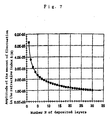
- the results shown in Fig. 7 are the results of calculations of the core refractive index from the average distribution in the case where the N is varied in the core having the refractive index distribution of (Formula 6).
- the core layer thickness a 6.5 ⁇ m
- ⁇ 0.0185.
- E-0.5 of the vertical axis of Fig. 7 means x10 -5 , and for example, 1.0E-0.5 means 1.0x10 -5 .
- the number of deposited layers of the core is set to 13 or more. Therefore, according to the third aspect of the invention, the standard deviation of the phase error distribution of the plurality of arrayed waveguides in the arrayed waveguide grating can be suppressed to 0.60rad or less. Furthermore, according to the third aspect of the invention, the standard deviation of the amount of fluctuation in the refractive index of the core of the arrayed waveguide can be securely suppressed to 4.84x10 -6 or less. Thereby, according to the third aspect of the invention, an arrayed waveguide grating can be provided in which low cross talk of 40dB or less is achieved.
- Fig. 1 is a constructional view of the main part which schematically shows the first embodiment of the arrayed waveguide grating relating to the invention
- Fig. 2 is a graph showing the results of measurement of transmission spectrum in the first and second embodiments of the arrayed waveguide grating
- Fig. 4 is a graph showing the relationship between the standard deviation ⁇ ( ⁇ ) of the phase error distribution and the cross talk
- Fig. 5 is an explanatory view showing the results of observation of fluctuations in the refractive index which occur like convex striate depending on the number of flame deposited layers.
- Fig. 6 is a graph showing the difference in refractive index distribution depending on the difference in the number of deposited layers of the core
- Fig. 7 is a graph showing the relationship between the number N of deposited layers of the core and the amount of fluctuation in the refractive index ⁇ n of the core
- Fig. 8 is a graph showing the results of measurement of the transmission spectrum of the third embodiment of the arrayed waveguide grating
- Fig. 9 is an explanatory view schematically showing the prior-art arrayed waveguide grating
- Fig. 10 is a graph showing the specific results of transmission spectrum of the prior-art arrayed waveguide grating.
- Fig. 1 is a constructional view of the main part of the first embodiment of the arrayed waveguide grating relating to the invention.
- optical waveguide part 10 having the waveguide composition shown in Fig. 1 is formed on silicon substrate 11.
- the feature of the present embodiment which is the point that is different from the prior-art example is that the number of deposited layers of the core forming the waveguide composition is set to 13, and the standard deviation of the amount of fluctuation in the refractive index of the core comprising all arrayed waveguides 14 is suppressed to 4.84x10 -6 or less. According to these arrangements, the standard deviation of the phase error distribution occurring within all arrayed waveguides 14 is suppressed to 0.6rad or less.
- a lower cladding layer (SiO 2 -B 2 O 3 -P 2 O 5 -based) is formed on the silicon substrate 11 by means of flame hydrolysis deposition and then consolidated, and a core layer (SiO 2 -B 2 O 3 -P 2 O 5 -GeO 2 -based) is formed on the lower cladding layer by means of flame hydrolysis deposition and then consolidated.
- the amount of material to be supplied to the core layer is set to be the same as that of 6-layer deposition in the prior-art, and accordingly, the speed of the burner for synthesizing fine glass particles when depositing the core layer is made to be double that of the prior-art (twice the speed when depositing 6 layers).
- the number of deposited layers of the core layer is set to 13.
- the photomask pattern is transferred onto the core layer by means of photolithography and reactive ion etching. Thereafter, cladding glass particles to be embedded are deposited on the core pattern by means of flame hydrolysis deposition, then consolidated, whereby an upper cladding layer is formed.
- the arrangement of the arrayed waveguide grating of the present embodiment was determined based on the results of examination by the present inventor (results of examination based on Fig. 3 through Fig. 7 and (Formula 1) through (Formula 8)) as mentioned above. That is, in the present embodiment, based on the abovementioned results of examination, the number of deposited layers of the core forming the waveguide composition including the arrayed waveguides 14 was set to 13, whereby the standard deviation of the amount of fluctuation in the refractive index of the core comprising all arrayed waveguides 14 was suppressed to 4.84x10 -6 or less. And, according to this arrangement, in the present embodiment, the standard deviation of the phase error distribution occurring within all arrayed waveguides 14 was suppressed to 0.6rad or less.
- the phase error of the arrayed waveguides 14 can be suppressed, and the cross talk can be suppressed to 40dB or less. Therefore, the arrayed waveguide grating of the present embodiment can satisfy the characteristics required for a D-WDM transmission system when it is applied to the D-WDM transmission system.
- Fig. 2 shows the transmission spectrum of the arrayed waveguide grating of the present embodiment. Also, as mentioned above, regarding this transmission spectrum, the transmission bandwidth is standardized by the FSR (Free Spectral Range:about 25nm herein), and the transmittance is standardized by means of the minimum loss.
- the cross talk which is the gap between the transmission loss (A of the figure) of the transmission wavelength and the background transmission loss (B of the figure) is significantly improved in comparison with the prior-art example. That is, although the cross talk of the prior-art arrayed waveguide grating is approximately 30dB, the cross talk of the arrayed waveguide grating of the present embodiment is approximately 40dB. According to the transmission spectrum of Fig. 2, it was confirmed that the cross talk of the arrayed waveguide grating of the present embodiment could be much improved compared with the case of the prior-art example.
- the second embodiment of the arrayed waveguide grating of the invention shall be described.
- the second embodiment is arranged in almost the same manner as in the abovementioned first embodiment.
- the feature of the second embodiment which is the point that is different from the first embodiment is that the deposition method of the core when manufacturing the arrayed waveguide grating is different from that of the first embodiment. That is, in the second embodiment, the amount of the material to be supplied to the core layer is set to be half of that of the prior-art 6-layer deposition, and the speed of the burner for synthesizing fine glass particles when depositing the core is made equal to the speed when depositing 6 layers in the prior-art, and the number of the deposited layers of the core is set to 13.
- the second embodiment is thus arranged, and when the transmission spectrum of the arrayed waveguide grating of the present embodiment was measured, the same result as that in Fig. 2 was obtained. Therefore, it was confirmed that the second embodiment has the same effect as in the first embodiment.
- the third embodiment is arranged in almost the same manner as in the abovementioned first embodiment.
- the feature of the third embodiment which is the point that is different from the abovementioned first and second embodiments is that the number of deposited layers of the core layer is set to 24.
- the amount of material to be supplied to the core layer is set to be a quarter of that of the prior-art 6-layer deposition, and the speed of the burner for synthesizing fine glass particles is set to be equal to the speed when depositing 6 layers in the prior-art.
- the present embodiment is thus arranged, and the transmission spectrum of the third embodiment is as shown in Fig. 8 .
- the cross talk which is the gap between the transmission loss (A of the figure) of the transmission wavelength and the background transmission loss (B of the figure) can be improved up to approximately 46dB.
- the present invention is not limited to the abovementioned embodiments, but various embodiments can be employed.
- the number of deposited layers of the core forming the waveguide composition including the arrayed waveguides 14 is set to 13 in the abovementioned first and second embodiments, and the number of deposited layers of the core is set to 24 in the third embodiment.
- the number of deposited layers of the core is not especially limited, but is set to a proper number of 13 or more.
- composition of the optical waveguide part 10 of the arrayed waveguide grating is not especially limited.
- the composition of the optical waveguide part 10 of the arrayed waveguide grating is properly set by using, for example, quartz as a main material.
- the arrayed waveguide grating of the invention since the phase error of light propagated in the arrayed waveguides can be suppressed by properly suppressing fluctuations in the refractive index of the plurality of arrayed waveguides, low cross talk of 40dB or less can be realized. Therefore, the arrayed waveguide grating of the invention is suitable as an optical transmission element for the D-WDM transmission system.
Landscapes
- Physics & Mathematics (AREA)
- Engineering & Computer Science (AREA)
- Microelectronics & Electronic Packaging (AREA)
- General Physics & Mathematics (AREA)
- Optics & Photonics (AREA)
- Optical Integrated Circuits (AREA)
Applications Claiming Priority (3)
| Application Number | Priority Date | Filing Date | Title |
|---|---|---|---|
| JP22661699 | 1999-08-10 | ||
| JP22661699 | 1999-08-10 | ||
| PCT/JP2000/005309 WO2001013150A1 (fr) | 1999-08-10 | 2000-08-08 | Selecteur de mode de diffraction de guides d'ondes en reseau |
Publications (2)
| Publication Number | Publication Date |
|---|---|
| EP1136852A1 EP1136852A1 (fr) | 2001-09-26 |
| EP1136852A9 true EP1136852A9 (fr) | 2001-11-28 |
Family
ID=16848005
Family Applications (1)
| Application Number | Title | Priority Date | Filing Date |
|---|---|---|---|
| EP00951897A Withdrawn EP1136852A1 (fr) | 1999-08-10 | 2000-08-08 | Selecteur de mode de diffraction de guides d'ondes en reseau |
Country Status (3)
| Country | Link |
|---|---|
| US (1) | US6442314B2 (fr) |
| EP (1) | EP1136852A1 (fr) |
| WO (1) | WO2001013150A1 (fr) |
Families Citing this family (15)
| Publication number | Priority date | Publication date | Assignee | Title |
|---|---|---|---|---|
| JP2001194541A (ja) * | 1999-05-31 | 2001-07-19 | Furukawa Electric Co Ltd:The | 光導波回路 |
| JP3566940B2 (ja) * | 2000-04-18 | 2004-09-15 | 古河電気工業株式会社 | アレイ導波路回折格子型光合分波器 |
| US6539150B2 (en) | 2000-12-13 | 2003-03-25 | Alcatel Optronics Uk Limited | Segmented waveguide flattening the passband of a phasar |
| GB0107111D0 (en) * | 2001-03-21 | 2001-05-09 | Bookham Technology Plc | Optical demultiplexer |
| JP2003075666A (ja) * | 2001-06-22 | 2003-03-12 | Furukawa Electric Co Ltd:The | アレイ導波路回折格子型光合分波器 |
| JP3884341B2 (ja) * | 2002-01-21 | 2007-02-21 | 古河電気工業株式会社 | 可変分散補償器およびその可変分散補償器を用いた可変分散補償デバイス |
| US7215841B2 (en) * | 2004-12-21 | 2007-05-08 | Intel Corporation | Extracting phase error in waveguides |
| JP2007065562A (ja) * | 2005-09-02 | 2007-03-15 | Furukawa Electric Co Ltd:The | アレイ導波路回折格子 |
| JP4748524B2 (ja) * | 2006-08-31 | 2011-08-17 | 古河電気工業株式会社 | アレイ導波路格子型合分波器 |
| JP5100175B2 (ja) * | 2007-03-28 | 2012-12-19 | 古河電気工業株式会社 | アレイ導波路格子型の合分波装置 |
| US20110085761A1 (en) * | 2009-05-26 | 2011-04-14 | Furukawa Electric Co., Ltd. | Arrayed waveguide grating and method of manufacturing arrayed waveguide grating |
| JP2010276639A (ja) * | 2009-05-26 | 2010-12-09 | Furukawa Electric Co Ltd:The | アレイ導波路格子 |
| CN102566090B (zh) | 2010-12-22 | 2014-12-10 | 李冰 | 一种光波导开关 |
| WO2012083862A1 (fr) | 2010-12-22 | 2012-06-28 | Bing Li | Photodétecteur à guide d'ondes et procédé de formation de celui-ci |
| CN102565932B (zh) | 2011-01-14 | 2014-10-08 | 李冰 | 色散校正的阵列波导光栅 |
Family Cites Families (2)
| Publication number | Priority date | Publication date | Assignee | Title |
|---|---|---|---|---|
| US5940548A (en) * | 1996-07-10 | 1999-08-17 | Nippon Telegraph And Telephone Corporation | Guided-wave circuit with optical characteristics adjusting plate, method for producing it, and apparatus for producing optical characteristics adjusting plate |
| US6229938B1 (en) * | 1999-02-01 | 2001-05-08 | Nippon Telegraph And Telephone Corporation | WDM filter |
-
2000
- 2000-08-08 EP EP00951897A patent/EP1136852A1/fr not_active Withdrawn
- 2000-08-08 WO PCT/JP2000/005309 patent/WO2001013150A1/fr not_active Ceased
-
2001
- 2001-04-10 US US09/828,827 patent/US6442314B2/en not_active Expired - Fee Related
Also Published As
| Publication number | Publication date |
|---|---|
| WO2001013150A9 (fr) | 2002-09-19 |
| US6442314B2 (en) | 2002-08-27 |
| EP1136852A1 (fr) | 2001-09-26 |
| US20010019644A1 (en) | 2001-09-06 |
| WO2001013150A1 (fr) | 2001-02-22 |
Similar Documents
| Publication | Publication Date | Title |
|---|---|---|
| US6853769B2 (en) | Arrayed waveguide grating with waveguides of unequal widths | |
| US6757454B2 (en) | Polarization desensitized optical waveguide interferometer | |
| EP1136852A9 (fr) | Selecteur de mode de diffraction de guides d'ondes en reseau | |
| CA2198836C (fr) | Multiplexeur-demultiplexeur optique | |
| US6731828B2 (en) | Waveguide-type optical signal processing circuit | |
| JP3615069B2 (ja) | アレイ導波路回折格子型光合分波器 | |
| US20010028762A1 (en) | Dispersion compensator and dispersion-compensating module employing the same | |
| US6904204B2 (en) | Array waveguide diffraction grating type optical multiplexer/demultiplexer | |
| US20020025133A1 (en) | Optical waveguide circuit | |
| US20030016928A1 (en) | Optical waveguide | |
| US6768840B2 (en) | Arrayed waveguide grating and method for manufacturing the same | |
| JP4833565B2 (ja) | 平面光導波路における偏光依存性の低減 | |
| US20020018622A1 (en) | Optical waveguide and method of manufacturing the same | |
| JP2003149479A (ja) | 石英系ガラス光導波路及びそれを用いた光モジュール | |
| WO2004061496A1 (fr) | Circuit multiplexeur/demultiplexeur optique du type a treillis de guides d'onde en reseau | |
| JP2001116939A (ja) | アレイ導波路回折格子 | |
| US7058262B2 (en) | Arrayed waveguide grating | |
| Han | Silicon Nitride Arrayed Waveguide Gratings | |
| Takahashi | Arrayed Waveguide Grating (AWG) | |
| JP2001091765A (ja) | アレイ導波路回折格子型光合分波器 | |
| JP2007093721A (ja) | 光波長合分波器 | |
| Wosinski et al. | Silicon-based integrated multiplexers for WDM systems | |
| JP2001066446A (ja) | アレイ導波路型回折格子 |
Legal Events
| Date | Code | Title | Description |
|---|---|---|---|
| PUAI | Public reference made under article 153(3) epc to a published international application that has entered the european phase |
Free format text: ORIGINAL CODE: 0009012 |
|
| 17P | Request for examination filed |
Effective date: 20010112 |
|
| AK | Designated contracting states |
Kind code of ref document: A1 Designated state(s): AT BE CH CY DE DK ES FI FR GB GR IE IT LI LU MC NL PT SE |
|
| RBV | Designated contracting states (corrected) |
Designated state(s): DE FR GB |
|
| A4 | Supplementary search report drawn up and despatched |
Effective date: 20050317 |
|
| RIC1 | Information provided on ipc code assigned before grant |
Ipc: 7G 02B 6/293 B Ipc: 7G 02B 6/132 B Ipc: 7G 02B 6/12 A Ipc: 7G 02B 6/34 B |
|
| 17Q | First examination report despatched |
Effective date: 20050513 |
|
| STAA | Information on the status of an ep patent application or granted ep patent |
Free format text: STATUS: THE APPLICATION IS DEEMED TO BE WITHDRAWN |
|
| 18D | Application deemed to be withdrawn |
Effective date: 20050926 |