EP1134898B1 - Carrier-dependent dithering for analog-to-digital conversion - Google Patents
Carrier-dependent dithering for analog-to-digital conversion Download PDFInfo
- Publication number
- EP1134898B1 EP1134898B1 EP01301944A EP01301944A EP1134898B1 EP 1134898 B1 EP1134898 B1 EP 1134898B1 EP 01301944 A EP01301944 A EP 01301944A EP 01301944 A EP01301944 A EP 01301944A EP 1134898 B1 EP1134898 B1 EP 1134898B1
- Authority
- EP
- European Patent Office
- Prior art keywords
- signal
- analog
- power level
- generate
- dither
- Prior art date
- Legal status (The legal status is an assumption and is not a legal conclusion. Google has not performed a legal analysis and makes no representation as to the accuracy of the status listed.)
- Expired - Lifetime
Links
- 238000006243 chemical reaction Methods 0.000 title description 8
- 230000001419 dependent effect Effects 0.000 title 1
- 239000000969 carrier Substances 0.000 claims description 18
- 238000000034 method Methods 0.000 claims description 7
- 230000001131 transforming effect Effects 0.000 claims description 3
- 238000001914 filtration Methods 0.000 claims 1
- 238000012546 transfer Methods 0.000 description 8
- 238000004458 analytical method Methods 0.000 description 7
- 238000013139 quantization Methods 0.000 description 5
- 238000012545 processing Methods 0.000 description 4
- 238000013461 design Methods 0.000 description 2
- 230000000694 effects Effects 0.000 description 2
- 238000005070 sampling Methods 0.000 description 2
- 238000012360 testing method Methods 0.000 description 2
- 238000011161 development Methods 0.000 description 1
- 238000010586 diagram Methods 0.000 description 1
- 238000013507 mapping Methods 0.000 description 1
- 238000012986 modification Methods 0.000 description 1
- 230000004048 modification Effects 0.000 description 1
- 238000001228 spectrum Methods 0.000 description 1
- 238000006467 substitution reaction Methods 0.000 description 1
Images

Classifications
-
- H—ELECTRICITY
- H03—ELECTRONIC CIRCUITRY
- H03M—CODING; DECODING; CODE CONVERSION IN GENERAL
- H03M1/00—Analogue/digital conversion; Digital/analogue conversion
- H03M1/06—Continuously compensating for, or preventing, undesired influence of physical parameters
-
- H—ELECTRICITY
- H03—ELECTRONIC CIRCUITRY
- H03M—CODING; DECODING; CODE CONVERSION IN GENERAL
- H03M1/00—Analogue/digital conversion; Digital/analogue conversion
- H03M1/06—Continuously compensating for, or preventing, undesired influence of physical parameters
- H03M1/0617—Continuously compensating for, or preventing, undesired influence of physical parameters characterised by the use of methods or means not specific to a particular type of detrimental influence
- H03M1/0634—Continuously compensating for, or preventing, undesired influence of physical parameters characterised by the use of methods or means not specific to a particular type of detrimental influence by averaging out the errors, e.g. using sliding scale
- H03M1/0636—Continuously compensating for, or preventing, undesired influence of physical parameters characterised by the use of methods or means not specific to a particular type of detrimental influence by averaging out the errors, e.g. using sliding scale in the amplitude domain
- H03M1/0639—Continuously compensating for, or preventing, undesired influence of physical parameters characterised by the use of methods or means not specific to a particular type of detrimental influence by averaging out the errors, e.g. using sliding scale in the amplitude domain using dither, e.g. using triangular or sawtooth waveforms
- H03M1/0641—Continuously compensating for, or preventing, undesired influence of physical parameters characterised by the use of methods or means not specific to a particular type of detrimental influence by averaging out the errors, e.g. using sliding scale in the amplitude domain using dither, e.g. using triangular or sawtooth waveforms the dither being a random signal
-
- H—ELECTRICITY
- H03—ELECTRONIC CIRCUITRY
- H03M—CODING; DECODING; CODE CONVERSION IN GENERAL
- H03M1/00—Analogue/digital conversion; Digital/analogue conversion
- H03M1/12—Analogue/digital converters
Definitions
- the present invention relates generally to analog-to-digital converters and, more particularly, relates to a technique for improving the accuracy of an analog-to-digital converter.
- ADCs analog-to-digital converters
- Analog-to-digital conversion involves amplitude quantization, where an analog input signal, which may vary continuously over a finite amplitude range, is sampled at a uniform sampling rate to map the analog input signal to a finite number of discrete amplitudes.
- the input signal dynamic range of an ADC is divided into a specified number of possible discrete amplitudes (i.e., quantization levels), where the number of discrete amplitude levels specifies the resolution of the ADC. For example, an ADC having 2 m quantization levels generates an m -bit digital output signal, where the value of m defines the resolution of the ADC.
- ADC ADC
- linearity or accuracy
- accuracy is a measure of the variance, from a straight line, of the ADC transfer function, i.e., the characteristic mapping of the input signal to the corresponding output signal.
- Non-linearity in an ADC transfer function typically results in conversion spurs, which are fictitious signals appearing in the frequency domain (e.g., during fast Fourier transform (FFT) analysis) of signals having discontinuities that are associated with deviations from a purely linear response.
- FFT fast Fourier transform
- Most existing techniques for increasing the accuracy of an ADC rely on analog domain methods to minimize the error due to the presence of internal and external noise sources, and to maximize the accuracy and the time and temperature stability of the analog components in the ADC.
- ADC for converting an analogue input signal (“Vin") into a digital output signal (“Digital Output”)
- the ADC comprising (a) a dither signal generator ("RNG”, “Dyn Dith DAC”), configured to generate an analogue dither signal ("dither”); (b) a signal coupler (Fig. 2: N1, N2), configured to add the analogue dither signal to the analogue input signal to generate a dithered analogue signal; (c) an amplitude quantizer (Fig. 2), configured to digitize the dithered analogue signal to generate the digital output signal; and (d) a processor (Fig. 1: “Comparator”, p. 131, col. 2, par. 1), configured to analyse the digital output signal to generate a control signal for controlling the amplitude of the dither signal generated by the dither signal generator.
- US-A-4857927 discloses an analogue-to-digital converter (Fig. 1) for converting an analogue input signal ("Input Signal") into a digital output signal (“Output Signal”), the ADC comprising (a) a dither signal generator (10, 12), configured to generate an analogue dither signal; (b) a signal coupler (14), configured to add the analogue dither signal to the analogue input signal to generate a dithered analogue signal; (c) an amplitude quantizer (16), configured to digitize the dithered analogue signal to generate the digital output signal; and (d) a processor (30), configured to analyse the digital output signal to generate a control signal ("Control Signal”) for controlling the amplitude of the dither signal generated by the dither signal generator.
- the present invention is directed to a technique for increasing the accuracy of an ADC.
- an analog dither signal is added to the analog input signal prior to amplitude quantization.
- the dither signal of the present invention has a variable amplitude that is controlled by a processor that analyzes the quantized digital representations of the dithered input signal to determine the appropriate amplitude for the dither signal to be added to the analog input signal.
- the amplitude of the dither signal is based on the power levels of one or more carriers present in the analog input signal.
- the addition of the dither signal reduces unwanted conversion spurs caused by non-linearities in the ADC transfer function.
- the present invention is an analog-to-digital converter (ADC) for converting an analog input signal into a digital output signal, comprising (a) a dither signal generator, configured to generate an analog dither signal; (b) a signal coupler, configured to add the analog dither signal to the analog input signal to generate a dithered analog signal; (c) an amplitude quantizer, configured to digitize the dithered analog signal to generate the digital output signal; and (d) a processor, configured to analyze the digital output signal to generate a control signal for controlling the amplitude of the dither signal generated by the dither signal generator, wherein the processor generates the control signal based on a measure of total instantaneous power level of one or more carriers in the analog input signal.
- ADC analog-to-digital converter
- the present invention is a method for converting an analog input signal into a digital output signal, comprising the steps of (a) generating an analog dither signal; (b) adding the analog dither signal to the analog input signal to generate a dithered analog signal; (c) digitizing the dithered analog signal to generate the digital output signal; and (d) analyze the digital output signal to generate a control signal for controlling the amplitude of the dither signal, wherein the control signal is based on a measure of total instantaneous power level of one or more carriers in the analog input signal.
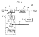
- an analog-to-digital converter (ADC) 100 comprises a signal coupler 101 , an amplitude quantizer 103 , a processor 105 , and a dither signal generator 107 .
- ADC 100 converts an analog input signal 102 into a digital output signal 106 .
- signal coupler 101 adds an analog dither signal 114 generated by dither signal generator 107 to the analog input signal 102 .
- the resulting dithered analog signal 104 is quantized by amplitude quantizer 103 to generate the digital output signal 106 .
- Processor 105 analyzes the digital output signal 106 to generate a control signal 108 used to control the amplitude of the analog dither signal 114 generated by dither signal generator 107 .
- the purpose of adding the dither signal 114 is to ensure that the resulting dithered analog signal 104 is an uncorrelated signal such that the digital output signal 106 has reduced conversion spurs due to non-linearity in the ADC transfer function.
- Signal coupler 101 may be any suitable component for adding the analog dither signal 114 to the analog input signal 102 , such as a passive component like a resistive or Wilkinson power divider or a directional or hybrid coupler, or an active component like a dual-gate FET or other transistor-based adder.
- Amplitude quantizer 103 may be any suitable component for quantizing a high-frequency analog signal. The sampling frequency of amplitude quantizer 103 should be at least two times the high-frequency limit of the ADC operational bandwidth.
- Processor 105 is any suitable digital processor, such as a digital signal processor (DSP) or a programmable logic device (PLD).
- DSP digital signal processor
- PLD programmable logic device
- ADC 100 is implemented as a single integrated circuit, although discrete-element implementations are also possible.
- dither signal generator 107 comprises a random noise source 109 , a variable gain amplifier (VGA) 111 , and a low-pass filter 113 .
- Random noise source 109 generates an analog random noise signal 110 .
- random noise source 109 may be based on one or more pseudo-random noise generators controlled by one or more digital circuits to generate digitally created noise, or it may be based on an analog noise source, such as a noise diode.
- VGA 111 amplifies the analog random noise signal 110 from random noise source 109 to generate an amplified analog noise signal 112 .
- the gain of VGA 111 is controlled by the control signal 108 from processor 105 .
- Low-pass filter 113 filters the amplified analog noise signal 112 from VGA 111 to generate the analog dither signal 114 for input to signal coupler 101 .
- low-pass filter 113 preferably limits the frequency of the analog dither signal to be a small fraction of the Nyquist tone for the bandwidth of ADC 100 .
- ADC 100 is designed to operate in the range from about 10-20 MHZ up to about 500 MHZ (or higher)
- low-pass filter 113 limits the frequency of the analog dither signal 114 to less than about 1 MHZ (i.e., about 1/20 to 1/10 of the low-frequency limit of the ADC operational bandwidth).
- Processor 105 processes every n th value in the digital output signal 106, where n is a positive integer, to identify and characterize the carriers that are present in the analog input signal 102 to generate the VGA control signal 108 .
- the amplitude of the dither signal 114 preferably corresponds to the sum of the power levels of the one or more carriers present within the ADC's operational bandwidth.
- FIG. 2 shows a flow chart of the processing implemented by processor 105 of FIG. 1 to generate the control signal 108 used to control VGA 111 , according to one embodiment of the present invention.
- Processor 105 samples the digital output signal 106 (step 201 of FIG. 2) and applies Fourier analysis (e.g., an FFT) to the sampled digital output signal (step 203 ).
- the low-frequency bins resulting from the FFT correspond to the dither signal 114
- the high-frequency FFT bins correspond to the input signal 102 .
- Processor 105 identifies each carrier in the input signal 102 as a significantly large peak in the magnitudes of the values maintained in the high-frequency FFT bins (step 205 ). This identification includes an identification of FFT bins corresponding to the low-frequency and high-frequency limits for each carrier, e.g., by thresholding the bin magnitude levels at a specified magnitude level or percentage of the carrier peak magnitude level.
- Processor 105 uses the results of the FFT analysis to calculate the total instantaneous power levels of the identified carriers in the input signal 102 and of the dither signal 114 (steps 207 and 209 , respectively).
- Processor 105 generates a value for control signal 108 in order to set the gain of VGA 111 to, for example, equalize the total instantaneous dither signal power level D(t) and the total instantaneous carrier power level S T (t) (step 211 ).
- the addition of such an dither signal 114 ensures that amplitude quantizer 103 sees a fairly uncorrelated signal power at the input so that the conversion spurs which result from non-linearities in the ADC transfer function will be reduced.
- the amplitude of the dither signal 114 can be updated to maintain the quality of the ADC digital output signal 1106 .
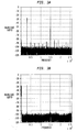
- FIGs. 3A and 3B illustrate exemplary test results indicating how the dither signal of the present invention can assist in reducing the effects of non-linearity in an ADC transfer function.
- FIG. 3A illustrates the 32k fast Fourier transform (FFT) analysis of the digital output signal generated by an ADC for an analog input signal having two different carriers (at about 3 MHZ and about 15 MHZ) without adding any dither signal.
- FIG. 3B illustrates a 32k FFT analysis of the digital output signal generated by an ADC for the same analog input signal, where a dither signal in accordance with the present invention is added prior to quantization. As shown in the figures, the addition of the dither signal eliminates conversion spurs evident in FIG. 3A, corresponding to improved quality of the digitized output spectrum, as shown in FIG. 3B.
- FFT fast Fourier transform
- the present invention may be applied in a variety of applications, including ADCs for input signals having one or more RF carriers containing or un-correlated data, such as TDMA, GSM, or CDMA applications.
- the dither signal may be of a relatively smaller amplitude as compared to the RF carriers.
Landscapes
- Engineering & Computer Science (AREA)
- Theoretical Computer Science (AREA)
- Analogue/Digital Conversion (AREA)
Applications Claiming Priority (2)
| Application Number | Priority Date | Filing Date | Title |
|---|---|---|---|
| US524152 | 2000-03-14 | ||
| US09/524,152 US6268814B1 (en) | 2000-03-14 | 2000-03-14 | Carrier-dependent dithering for analog-to-digital conversion |
Publications (3)
| Publication Number | Publication Date |
|---|---|
| EP1134898A2 EP1134898A2 (en) | 2001-09-19 |
| EP1134898A3 EP1134898A3 (en) | 2004-01-07 |
| EP1134898B1 true EP1134898B1 (en) | 2007-01-10 |
Family
ID=24087981
Family Applications (1)
| Application Number | Title | Priority Date | Filing Date |
|---|---|---|---|
| EP01301944A Expired - Lifetime EP1134898B1 (en) | 2000-03-14 | 2001-03-05 | Carrier-dependent dithering for analog-to-digital conversion |
Country Status (9)
| Country | Link |
|---|---|
| US (1) | US6268814B1 (ja) |
| EP (1) | EP1134898B1 (ja) |
| JP (1) | JP3836328B2 (ja) |
| KR (1) | KR100787369B1 (ja) |
| CN (1) | CN1317880A (ja) |
| AU (1) | AU2645401A (ja) |
| BR (1) | BR0100945A (ja) |
| CA (1) | CA2336728A1 (ja) |
| DE (1) | DE60125851T2 (ja) |
Families Citing this family (44)
| Publication number | Priority date | Publication date | Assignee | Title |
|---|---|---|---|---|
| WO2000044098A1 (en) * | 1999-01-19 | 2000-07-27 | Steensgaard Madsen Jesper | Residue-compensating a / d converter |
| US6331831B1 (en) * | 1999-11-12 | 2001-12-18 | At&T Corp. | A/D conversion through dithering |
| US6704673B2 (en) * | 2002-08-06 | 2004-03-09 | Agilent Technologies, Inc. | System and method for improving linearity and reducing digitization artifacts in a data analysis system |
| US6906649B2 (en) * | 2003-08-06 | 2005-06-14 | Micronetics, Inc | Dithering module with diplexer |
| US20050057381A1 (en) * | 2003-08-06 | 2005-03-17 | Micronetics, Inc. | Dithering module with diplexer |
| US6950048B1 (en) * | 2004-04-02 | 2005-09-27 | Tektronix, Inc. | Dither system for a quantizing device |
| US7652723B1 (en) | 2004-04-19 | 2010-01-26 | Video Accessory Corporation | Composite video signal correction unit for video imaging and video recording systems |
| US6980145B1 (en) * | 2004-07-30 | 2005-12-27 | Broadcom Corporation | System and method for noise cancellation in a signal processing circuit |
| US7015851B1 (en) * | 2004-10-26 | 2006-03-21 | Agilent Technologies, Inc. | Linearizing ADCs using single-bit dither |
| US7362250B2 (en) * | 2005-01-31 | 2008-04-22 | Texas Instruments Incorporated | Dynamic dither for sigma-delta converters |
| US7161511B2 (en) * | 2005-06-03 | 2007-01-09 | General Electric Company | Linearization system and method |
| US7460043B2 (en) * | 2005-06-03 | 2008-12-02 | General Electric Company | Analog-to-digital converter compensation system and method |
| US7116262B1 (en) * | 2005-06-30 | 2006-10-03 | Sigmatel, Inc. | System and method to receive data |
| KR100719370B1 (ko) * | 2005-08-03 | 2007-05-17 | 삼성전자주식회사 | 아날로그-디지털 변환기 및 이를 포함하는 씨모스 이미지센서, 그리고 씨모스 이미지 센서의 동작 방법 |
| US7224299B2 (en) * | 2005-09-30 | 2007-05-29 | Nxp, B.V. | System and method for adjusting dither in a delta sigma modulator |
| EP2003783A4 (en) * | 2006-03-31 | 2011-03-09 | Nihon Dempa Kogyo Co | DIGITAL PROCESSING DEVICE |
| US7554471B2 (en) * | 2006-11-01 | 2009-06-30 | Northrop Grumman Corporation | System and method for improving linearity of a DAC |
| US7456773B1 (en) * | 2007-06-14 | 2008-11-25 | Qualcomm Incorporated | Pseudo-differential class-AB digital-to-analog converter with code dependent DC current |
| JP4627078B2 (ja) * | 2007-10-25 | 2011-02-09 | ルネサスエレクトロニクス株式会社 | デジタルアナログ変換回路とデータドライバ及び表示装置 |
| CN101458950B (zh) * | 2007-12-14 | 2011-09-14 | 安凯(广州)微电子技术有限公司 | 一种消除模数转换器噪声对数字录音干扰的方法 |
| US7602324B1 (en) * | 2009-01-20 | 2009-10-13 | Himax Media Solutions, Inc. | A/D converter and method for converting analog signals into digital signals |
| JP2010199799A (ja) * | 2009-02-24 | 2010-09-09 | Renesas Electronics Corp | アナログデジタル変換回路 |
| US7973612B2 (en) * | 2009-04-26 | 2011-07-05 | Qualcomm Incorporated | Supply-regulated phase-locked loop (PLL) and method of using |
| CN101800560B (zh) * | 2010-03-17 | 2012-10-17 | 苏州国芯科技有限公司 | Flash控制器中BCH编译码的纠错能力扩展方法 |
| US8477053B2 (en) * | 2011-06-06 | 2013-07-02 | Analog Devices, Inc. | ADC with resolution detector and variable dither |
| US8723707B2 (en) * | 2011-11-14 | 2014-05-13 | Analog Devices, Inc. | Correlation-based background calibration for reducing inter-stage gain error and non-linearity in pipelined analog-to-digital converters |
| DK177939B1 (en) * | 2012-12-18 | 2015-01-19 | Miitors Aps | A method for linearization of the output of an analog-to-digital converter and measuring instruments using such method |
| RU2548658C1 (ru) * | 2013-10-03 | 2015-04-20 | Акционерное общество "Концерн "Созвездие" | Радиоприемное устройство с ключевым управлением амплитудой размывающего сигнала |
| CN103560800B (zh) * | 2013-11-04 | 2015-12-02 | 中国电子科技集团公司第四十一研究所 | 一种提高adc+fpga数字接收系统灵敏度的抖动发生装置及抖动产生方法 |
| US9077363B2 (en) | 2013-12-03 | 2015-07-07 | Analog Devices, Inc. | Stochastic encoding in analog to digital conversion |
| CN103634005B (zh) * | 2013-12-13 | 2017-06-06 | 戴祖渝 | 一种模数转换器中量化噪声随机化的方法 |
| US9337937B2 (en) * | 2014-03-10 | 2016-05-10 | Cisco Technology, Inc. | Common mode rejection ratio control for coherent optical receivers |
| DE102014204518A1 (de) | 2014-03-12 | 2015-09-17 | Siemens Aktiengesellschaft | Schaltungsanordnung, Analog-Digital-Wandler, Gradientenverstärker und Verfahren zur Unterdrückung von Offset, Offsetdrift und 1/f-Rauschen einer der Analog-Digital-Konvertierung |
| FR3037456B1 (fr) * | 2015-06-10 | 2017-06-02 | Thales Sa | Procede de synthese d'un bruit analogique, synthetiseur de bruit et chaine de codage utilisant un tel synthetiseur |
| DE102016204417A1 (de) * | 2016-03-17 | 2017-09-21 | Continental Teves Ag & Co. Ohg | Vorrichtung zum Messen einer Messgröße |
| JP7078347B2 (ja) * | 2016-04-01 | 2022-05-31 | 株式会社ジェイテクト | センサ装置 |
| RU2660660C2 (ru) * | 2016-04-11 | 2018-07-09 | Акционерное общество "Концерн "Созвездие" | Радиоприёмное устройство с ключевым управлением амплитудой размывающего сигнала |
| CN106788433B (zh) * | 2016-12-13 | 2019-07-05 | 山东大学 | 数字噪声源、数据处理系统及数据处理方法 |
| RU181983U1 (ru) * | 2016-12-29 | 2018-07-31 | Открытое акционерное общество "Научно-производственное объединение Ангстрем" | Приемное устройство с увеличенным динамическим диапазоном |
| US10116322B1 (en) | 2017-12-01 | 2018-10-30 | Raytheon Company | Rail adaptive dither |
| CN108111759A (zh) * | 2017-12-23 | 2018-06-01 | 航天恒星科技有限公司 | 面向面阵ccd光电转换的仿真设计方法 |
| US11652491B2 (en) * | 2020-08-07 | 2023-05-16 | Analog Devices International Unlimited Company | High-pass shaped dither in continuous-time residue generation systems for analog-to-digital converters |
| CN114252160B (zh) * | 2020-09-22 | 2024-03-22 | 无锡华润上华科技有限公司 | 模数转换器及热电堆阵列 |
| US11949426B2 (en) * | 2020-12-16 | 2024-04-02 | Qualcomm Incorporated | Configurable analog-to-digital conversion parameters |
Family Cites Families (11)
| Publication number | Priority date | Publication date | Assignee | Title |
|---|---|---|---|---|
| US4710747A (en) * | 1984-03-09 | 1987-12-01 | Fairchild Semiconductor Corporation | Method and apparatus for improving the accuracy and resolution of an analog-to-digital converter (ADC) |
| JPS62112221U (ja) * | 1985-12-27 | 1987-07-17 | ||
| JP3168620B2 (ja) * | 1991-07-03 | 2001-05-21 | ソニー株式会社 | ディジタル/アナログ変換装置 |
| US5189418A (en) * | 1992-04-16 | 1993-02-23 | Hewlett-Packard Company | Dither error correction |
| US5940138A (en) * | 1992-08-04 | 1999-08-17 | J. Carl Cooper | Analog signal process with dither pattern |
| US5493298A (en) * | 1993-03-01 | 1996-02-20 | Hewlett-Packard Company | Dithered analog-to-digital converter |
| US5745061A (en) * | 1995-07-28 | 1998-04-28 | Lucent Technologies Inc. | Method of improving the stability of a sigma-delta modulator employing dither |
| US5745274A (en) * | 1995-12-27 | 1998-04-28 | Lucent Technologies Inc. | Maintenance of optical networks |
| DE19720548C2 (de) * | 1997-05-16 | 2003-07-10 | Rohde & Schwarz | Analog/Digital-Wandler |
| US5963157A (en) * | 1997-06-23 | 1999-10-05 | Motorola, Inc. | Method and apparatus for the addition and removal of a dither signal |
| US6016113A (en) * | 1997-06-26 | 2000-01-18 | Binder; Yehuda | System for enhancing the accuracy of analog-digital-analog conversions |
-
2000
- 2000-03-14 US US09/524,152 patent/US6268814B1/en not_active Expired - Lifetime
-
2001
- 2001-02-14 CA CA002336728A patent/CA2336728A1/en not_active Abandoned
- 2001-03-05 DE DE60125851T patent/DE60125851T2/de not_active Expired - Lifetime
- 2001-03-05 EP EP01301944A patent/EP1134898B1/en not_active Expired - Lifetime
- 2001-03-06 JP JP2001061238A patent/JP3836328B2/ja not_active Expired - Fee Related
- 2001-03-09 BR BR0100945-1A patent/BR0100945A/pt not_active Application Discontinuation
- 2001-03-09 AU AU26454/01A patent/AU2645401A/en not_active Abandoned
- 2001-03-13 CN CN01111823A patent/CN1317880A/zh active Pending
- 2001-03-14 KR KR1020010013119A patent/KR100787369B1/ko not_active IP Right Cessation
Also Published As
| Publication number | Publication date |
|---|---|
| US6268814B1 (en) | 2001-07-31 |
| EP1134898A2 (en) | 2001-09-19 |
| DE60125851D1 (de) | 2007-02-22 |
| KR20010092323A (ko) | 2001-10-24 |
| EP1134898A3 (en) | 2004-01-07 |
| KR100787369B1 (ko) | 2007-12-24 |
| CA2336728A1 (en) | 2001-09-14 |
| DE60125851T2 (de) | 2007-10-11 |
| BR0100945A (pt) | 2001-10-30 |
| JP2001267922A (ja) | 2001-09-28 |
| JP3836328B2 (ja) | 2006-10-25 |
| AU2645401A (en) | 2001-09-20 |
| CN1317880A (zh) | 2001-10-17 |
Similar Documents
| Publication | Publication Date | Title |
|---|---|---|
| EP1134898B1 (en) | Carrier-dependent dithering for analog-to-digital conversion | |
| Kester | Mixed-signal and DSP design techniques | |
| US5659312A (en) | Method and apparatus for testing digital to analog and analog to digital converters | |
| US8508395B2 (en) | Time varying quantization-based linearity enhancement of signal converters and mixed-signal systems | |
| KR100367339B1 (ko) | 디지탈논리게이트코어를갖는시그마-델타변환기 | |
| US5416481A (en) | Analog-to-digital converter with multi-level dither current input | |
| US20170187387A1 (en) | Input path matching in pipelined continuous-time analog-to-digital converters | |
| US11652491B2 (en) | High-pass shaped dither in continuous-time residue generation systems for analog-to-digital converters | |
| US4843390A (en) | Oversampled A/D converter having digital error correction | |
| Eielsen et al. | Improving digital-to-analog converter linearity by large high-frequency dithering | |
| US8212699B1 (en) | System and method for extending the overload range of a sigma delta ADC system by providing over-range quantization levels | |
| US20150035691A1 (en) | Method and related device for generating a digital output signal corresponding to an analog input signal | |
| Eielsen et al. | Existing methods for improving the accuracy of digital-to-analog converters | |
| CN213547830U (zh) | 用于电路部件的自适应动态元件匹配的装置 | |
| US10348321B2 (en) | Digital analog dither adjustment | |
| KR20150077420A (ko) | 변환기 | |
| Adamo et al. | Measuring the static characteristic of dithered A/D converters | |
| Lyons et al. | Reducing ADC quantization noise | |
| Caza-Szoka et al. | Low group delay interpolation filter for Delta-Sigma converters | |
| Otsu et al. | High-Precision Evaluation System Using High-Order Digital Δ∑ Modulator for Digital Audio System | |
| Michaeli et al. | Parameters of band pass ΣΔ-ADC and the comparison with the standard ones | |
| Devices | Mixed-signal and DSP design techniques | |
| Kester et al. | Sampled Data Systems | |
| CN116865755A (zh) | 一种应用于具有前端采保结构的流水线adc线性化校准电路及校准方法 | |
| US6779005B2 (en) | Method and device for detecting random missing code |
Legal Events
| Date | Code | Title | Description |
|---|---|---|---|
| PUAI | Public reference made under article 153(3) epc to a published international application that has entered the european phase |
Free format text: ORIGINAL CODE: 0009012 |
|
| AK | Designated contracting states |
Kind code of ref document: A2 Designated state(s): AT BE CH CY DE DK ES FI FR GB GR IE IT LI LU MC NL PT SE TR |
|
| AX | Request for extension of the european patent |
Free format text: AL;LT;LV;MK;RO;SI |
|
| PUAL | Search report despatched |
Free format text: ORIGINAL CODE: 0009013 |
|
| AK | Designated contracting states |
Kind code of ref document: A3 Designated state(s): AT BE CH CY DE DK ES FI FR GB GR IE IT LI LU MC NL PT SE TR |
|
| AX | Request for extension of the european patent |
Extension state: AL LT LV MK RO SI |
|
| 17P | Request for examination filed |
Effective date: 20040626 |
|
| AKX | Designation fees paid |
Designated state(s): DE FI FR GB SE |
|
| GRAP | Despatch of communication of intention to grant a patent |
Free format text: ORIGINAL CODE: EPIDOSNIGR1 |
|
| RTI1 | Title (correction) |
Free format text: CARRIER-DEPENDENT DITHERING FOR ANALOG-TO-DIGITAL CONVERSION |
|
| GRAS | Grant fee paid |
Free format text: ORIGINAL CODE: EPIDOSNIGR3 |
|
| GRAA | (expected) grant |
Free format text: ORIGINAL CODE: 0009210 |
|
| AK | Designated contracting states |
Kind code of ref document: B1 Designated state(s): DE FI FR GB SE |
|
| PG25 | Lapsed in a contracting state [announced via postgrant information from national office to epo] |
Ref country code: FI Free format text: LAPSE BECAUSE OF FAILURE TO SUBMIT A TRANSLATION OF THE DESCRIPTION OR TO PAY THE FEE WITHIN THE PRESCRIBED TIME-LIMIT Effective date: 20070110 |
|
| REG | Reference to a national code |
Ref country code: GB Ref legal event code: FG4D |
|
| REF | Corresponds to: |
Ref document number: 60125851 Country of ref document: DE Date of ref document: 20070222 Kind code of ref document: P |
|
| PG25 | Lapsed in a contracting state [announced via postgrant information from national office to epo] |
Ref country code: SE Free format text: LAPSE BECAUSE OF FAILURE TO SUBMIT A TRANSLATION OF THE DESCRIPTION OR TO PAY THE FEE WITHIN THE PRESCRIBED TIME-LIMIT Effective date: 20070410 |
|
| ET | Fr: translation filed | ||
| PLBE | No opposition filed within time limit |
Free format text: ORIGINAL CODE: 0009261 |
|
| STAA | Information on the status of an ep patent application or granted ep patent |
Free format text: STATUS: NO OPPOSITION FILED WITHIN TIME LIMIT |
|
| 26N | No opposition filed |
Effective date: 20071011 |
|
| REG | Reference to a national code |
Ref country code: GB Ref legal event code: 732E Free format text: REGISTERED BETWEEN 20131031 AND 20131106 |
|
| REG | Reference to a national code |
Ref country code: FR Ref legal event code: CD Owner name: ALCATEL-LUCENT USA INC. Effective date: 20131122 |
|
| REG | Reference to a national code |
Ref country code: FR Ref legal event code: GC Effective date: 20140410 |
|
| REG | Reference to a national code |
Ref country code: FR Ref legal event code: RG Effective date: 20141015 |
|
| REG | Reference to a national code |
Ref country code: FR Ref legal event code: PLFP Year of fee payment: 15 |
|
| REG | Reference to a national code |
Ref country code: FR Ref legal event code: PLFP Year of fee payment: 16 |
|
| REG | Reference to a national code |
Ref country code: FR Ref legal event code: PLFP Year of fee payment: 17 |
|
| REG | Reference to a national code |
Ref country code: FR Ref legal event code: PLFP Year of fee payment: 18 |
|
| PGFP | Annual fee paid to national office [announced via postgrant information from national office to epo] |
Ref country code: DE Payment date: 20190219 Year of fee payment: 19 Ref country code: GB Payment date: 20190227 Year of fee payment: 19 |
|
| PGFP | Annual fee paid to national office [announced via postgrant information from national office to epo] |
Ref country code: FR Payment date: 20190213 Year of fee payment: 19 |
|
| REG | Reference to a national code |
Ref country code: DE Ref legal event code: R119 Ref document number: 60125851 Country of ref document: DE |
|
| PG25 | Lapsed in a contracting state [announced via postgrant information from national office to epo] |
Ref country code: DE Free format text: LAPSE BECAUSE OF NON-PAYMENT OF DUE FEES Effective date: 20201001 Ref country code: FR Free format text: LAPSE BECAUSE OF NON-PAYMENT OF DUE FEES Effective date: 20200331 |
|
| GBPC | Gb: european patent ceased through non-payment of renewal fee |
Effective date: 20200305 |
|
| PG25 | Lapsed in a contracting state [announced via postgrant information from national office to epo] |
Ref country code: GB Free format text: LAPSE BECAUSE OF NON-PAYMENT OF DUE FEES Effective date: 20200305 |