EP1134659A2 - Redundanz-Multiplexer für Halbleiterspeicheranordnung - Google Patents
Redundanz-Multiplexer für Halbleiterspeicheranordnung Download PDFInfo
- Publication number
- EP1134659A2 EP1134659A2 EP01104907A EP01104907A EP1134659A2 EP 1134659 A2 EP1134659 A2 EP 1134659A2 EP 01104907 A EP01104907 A EP 01104907A EP 01104907 A EP01104907 A EP 01104907A EP 1134659 A2 EP1134659 A2 EP 1134659A2
- Authority
- EP
- European Patent Office
- Prior art keywords
- bit lines
- redundancy
- multiplexer
- switches
- control
- Prior art date
- Legal status (The legal status is an assumption and is not a legal conclusion. Google has not performed a legal analysis and makes no representation as to the accuracy of the status listed.)
- Granted
Links
- 239000004065 semiconductor Substances 0.000 title claims description 8
- 230000002950 deficient Effects 0.000 claims description 5
- 230000006870 function Effects 0.000 description 1
Images
Classifications
-
- G—PHYSICS
- G11—INFORMATION STORAGE
- G11C—STATIC STORES
- G11C29/00—Checking stores for correct operation ; Subsequent repair; Testing stores during standby or offline operation
- G11C29/70—Masking faults in memories by using spares or by reconfiguring
- G11C29/78—Masking faults in memories by using spares or by reconfiguring using programmable devices
- G11C29/84—Masking faults in memories by using spares or by reconfiguring using programmable devices with improved access time or stability
- G11C29/846—Masking faults in memories by using spares or by reconfiguring using programmable devices with improved access time or stability by choosing redundant lines at an output stage
Definitions
- the present invention relates to a redundancy multiplexer for a semiconductor memory device to replace two faulty bit lines due to two redundant bit lines, with the information stored in fuses, which bit lines are to be replaced in a decoder control or switching signals are generated, and in which two redundancy areas with the redundant bit lines on both sides selectable to a central bus from the control or switching signal are.
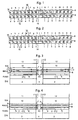
- Fig. 4 shows the structure of a conventional redundancy multiplexer for a semiconductor memory device.
- I / O input / output unit
- Fig. 4 shows the structure of a conventional redundancy multiplexer for a semiconductor memory device.
- I / O input / output unit
- This information about faulty bit lines is stored in fuses (FUSES) 3, so that coded here Fuse information CFI is present, which indicates which bit lines are faulty and replaced by redundant bit lines Need to become.
- the one in FIG. 4 to the right of the Central bus 1 located 3 fuses the coded fuse information CFI via the buffer and decoder 5, which decoded it Fuse information FI generated to the control unit 6 sent and from this across the entire interface width of the redundancy multiplexer 9 distributed before the associated redundant bit line in an area 11 next to a sense amplifier (SSA) following memory cell array 13 driven becomes.
- SSA sense amplifier
- This task is the beginning of a redundancy multiplexer mentioned type according to the invention solved in that by Comparison of the two control or switching signals to each two consecutive switches of the multiplexer found is whether the switch corresponding to the number of defective bit lines are correct.
- the redundancy multiplexer thus lies comparators between two provided in series with each other Switches. These comparators compare with that Control or switching signal the decoded sent to each switch Address ("1" or "0") and swap if necessary these addresses, if necessary, so that the incorrect address closer to the central redundancy areas is that controls switches that are closer to the memory cell array are. Only if this condition is met no data is read from faulty bit lines. On Such erroneous reading can be done by swapping the Addresses excluded using the comparators between the switches become.
- the error is stored necessary in the tester because the order of the replacements is determined must be burned before fuses can be burned. At this sequence is determined directly in the present invention, so that a fuse can be burned immediately if an error occurs.
- a redundancy multiplexer 8 or 9, as shown in FIGS. 1 and 2 can be seen from a large number of switches 14, can have positions (0) and (1).
- this Switches 14 are fed data which form bit lines, connected to outputs 16 of multiplexer 9 are to be forwarded.
- Now become faulty Bit lines "X" are determined by the of a Decoder 5 (see FIGS. 3 and 4) supplied control or Switch signals, the switches 14 controlled so that in Fig. 1st those on the left of the faulty bit lines "X" Bit lines take on their function, this taking over down to the redundant bit lines in the area of the central bus 1 is pushed on. To do this, take the corresponding switch 14 to position (1).
- Fig. 2 shows the same arrangement as Fig. 1 except that that the switches in the right half with the connections "i" to "p" of the redundancy multiplexer 9 or the multiplexer 8 positions (1,1,1,1,0,0,0,0; 1,1,1,0,0,0,0,0) instead of (1,1,1,0,0,0,0,0; 1,1,1,1,0,0,0,0).
- Words in the case of the connection "1" of the multiplexer 8 connected switches 14 are in Fig. 2 the control or Switching signals or "addresses" (0) and (1) for the multiplexers 8 and 9, while in Fig. 1 these switching or control signals have the values (1) and (0).
- the address at this switch 14 occurs when reading of the memory cell array a faulty bit line "X" of the Multiplexers 8 in appearance.
- this undesirable result can thereby be prevented that the individual control or switching signals or addresses (1) and (0) compared with one another and, if appropriate be exchanged so that the faulty one Address that is closer to the central redundancy areas 11, 12 is located ("(1)" at port 1 of multiplexer 9) Controls switches that are closer to the memory cell array.
- the invention thus reliably ensures that no errors when reading the memory cell array 13 Bit lines "X" appear.
Landscapes
- For Increasing The Reliability Of Semiconductor Memories (AREA)
- Techniques For Improving Reliability Of Storages (AREA)
Abstract
Description
- Fig. 1
- ein Ausführungsbeispiel des erfindungsgemäßen Redundanz-Multiplexers mit richtiger Zuordnung der Adressen,
- Fig. 2
- den Multiplexer von Fig. 1 mit unrichtiger Zuordnung der Adressen,
- Fig. 3
- eine schematische Darstellung des erfindungsgemäßen Redundanz-Multiplexers für eine Halbleiterspeicheranordnung und
- Fig. 4
- eine schematische Darstellung eines bestehenden Redundanz-Multiplexers für eine Halbleiterspeicheranordnung.
Claims (3)
- Redundanz-Multiplexer für Halbleiterspeicheranordnung zum Ersetzen von zwei fehlerhaften Bitleitungen (X) durch zwei redundante Bitleitungen, bei dem aus in Fuses (3) abgespeicherter Information, welche Bitleitungen zu ersetzen sind, in einem Decoder (5) Steuer- bzw. Schaltsignale (4) erzeugt werden, und bei dem zwei Redundanz-Bereiche (11, 12) mit den redundanten Bitleitungen beidseitig zu einem Zentralbus (1) von dem Steuer- bzw. Schaltsignal auswählbar sind,
dadurch gekennzeichnet, daß durch Vergleich der beiden Steuer- bzw. Schaltsignale zu jeweils zwei hintereinander liegenden Schaltern (14) des Multiplexers (8, 9) festgestellt wird, ob die Schalter (14) entsprechend der Anzahl der fehlerhaften Bitleitungen richtig gestellt sind. - Redundanz-Multiplexer nach Anspruch 1,
dadurch gekennzeichnet, daß zwischen jeweils zwei Schaltern (14) des Redundanz-Multiplexers ein Vergleicher (17) vorgesehen ist. - Redundanz-Multiplexer nach Anspruch 1 oder 2,
dadurch gekennzeichnet, daß die Schalter (14) derart gestellt sind, daß ein fehlerhaftes Steuer- bzw. Schaltsignal mit einer Adresse, die näher bei den zentralen Redundanz-Bereichen gelegen ist, die Schalter (14) steuert, die näher bei einem Speicherzellenfeld (13) angeordnet sind.
Applications Claiming Priority (2)
| Application Number | Priority Date | Filing Date | Title |
|---|---|---|---|
| DE10012104A DE10012104C2 (de) | 2000-03-13 | 2000-03-13 | Redundanz-Multiplexer für Halbleiterspeicheranordnung |
| DE10012104 | 2000-03-13 |
Publications (3)
| Publication Number | Publication Date |
|---|---|
| EP1134659A2 true EP1134659A2 (de) | 2001-09-19 |
| EP1134659A3 EP1134659A3 (de) | 2002-06-05 |
| EP1134659B1 EP1134659B1 (de) | 2005-10-19 |
Family
ID=7634498
Family Applications (1)
| Application Number | Title | Priority Date | Filing Date |
|---|---|---|---|
| EP01104907A Expired - Lifetime EP1134659B1 (de) | 2000-03-13 | 2001-02-28 | Redundanz-Multiplexer für Halbleiterspeicheranordnung |
Country Status (4)
| Country | Link |
|---|---|
| US (1) | US6574155B2 (de) |
| EP (1) | EP1134659B1 (de) |
| DE (2) | DE10012104C2 (de) |
| TW (1) | TW504697B (de) |
Family Cites Families (6)
| Publication number | Priority date | Publication date | Assignee | Title |
|---|---|---|---|---|
| JP2837433B2 (ja) * | 1989-06-05 | 1998-12-16 | 三菱電機株式会社 | 半導体記憶装置における不良ビット救済回路 |
| JP2600018B2 (ja) * | 1990-09-29 | 1997-04-16 | 三菱電機株式会社 | 半導体記憶装置 |
| DE69320824T2 (de) * | 1993-12-09 | 1999-05-12 | Stmicroelectronics S.R.L., Agrate Brianza, Mailand/Milano | Integrierte Schaltung zur Überwachung der Benutzung von Redunanzspeicherbauelementen in einer Halbleiterspeichereinrichtung |
| JP3501893B2 (ja) * | 1996-02-23 | 2004-03-02 | 株式会社 沖マイクロデザイン | 半導体記憶装置 |
| US6118727A (en) * | 1998-03-10 | 2000-09-12 | Cypress Semiconductor Corporation | Semiconductor memory with interdigitated array having bit line pairs accessible from either of two sides of the array |
| US6363020B1 (en) * | 1999-12-06 | 2002-03-26 | Virage Logic Corp. | Architecture with multi-instance redundancy implementation |
-
2000
- 2000-03-13 DE DE10012104A patent/DE10012104C2/de not_active Expired - Fee Related
-
2001
- 2001-02-28 DE DE50107725T patent/DE50107725D1/de not_active Expired - Fee Related
- 2001-02-28 EP EP01104907A patent/EP1134659B1/de not_active Expired - Lifetime
- 2001-03-13 US US09/805,295 patent/US6574155B2/en not_active Expired - Lifetime
- 2001-04-12 TW TW090105688A patent/TW504697B/zh not_active IP Right Cessation
Also Published As
| Publication number | Publication date |
|---|---|
| DE50107725D1 (de) | 2005-11-24 |
| DE10012104A1 (de) | 2001-09-27 |
| US20010021132A1 (en) | 2001-09-13 |
| TW504697B (en) | 2002-10-01 |
| DE10012104C2 (de) | 2002-05-02 |
| US6574155B2 (en) | 2003-06-03 |
| EP1134659B1 (de) | 2005-10-19 |
| EP1134659A3 (de) | 2002-06-05 |
Similar Documents
| Publication | Publication Date | Title |
|---|---|---|
| DE69428418T2 (de) | Halbleiterspeichergerät mit einem Ersatzspeicherzellfeld | |
| DE69019697T2 (de) | Reparierbare Speicherschaltung. | |
| DE3638632C2 (de) | ||
| DE3111447C2 (de) | ||
| DE69411532T2 (de) | Verfahren zur Programmierung von Redundanzregistern in einer Zeilenredundanzschaltung für einen Halbleiterspeicherbaustein | |
| DE68924639T2 (de) | Matrixspeicher, der Standardblöcke, Standard-Unterblöcke, einen redundanten Block und redundante Unterblöcke beinhaltet, und integrierter Kreis, der eine Vielzahl solcher Matrixspeicher beinhaltet. | |
| DE4028819A1 (de) | Schaltungsanordnung zum testen eines halbleiterspeichers mittels paralleltests mit verschiedenen testbitmustern | |
| DE10206689A1 (de) | Integrierter Speicher und Verfahren zum Betrieb eines integrierten Speichers | |
| DE3827174A1 (de) | Halbleiter-speichervorrichtung | |
| DE10257337A1 (de) | System und Verfahren zum Speichern von Paritätsinformationen in Sicherungen | |
| EP0186040A1 (de) | Integrierter Halbleiterspeicher | |
| EP0965995B1 (de) | Schaltungsanordnung und Verfahren zur automatischen Erkennung und Beseitigung von Wortleitungs-Bitleitungs-Kurzschlüssen | |
| EP0214508B1 (de) | Integrierter Halbleiterspeicher | |
| EP1134659B1 (de) | Redundanz-Multiplexer für Halbleiterspeicheranordnung | |
| EP0579327B1 (de) | Integrierter Matrixspeicher mit einer Schaltungsanordnung zum Prüfen der Adressierung | |
| DE19924153B4 (de) | Schaltungsanordnung zur Reparatur eines Halbleiterspeichers | |
| DE69000302T2 (de) | Redundanzschaltung mit speicherung der position des ausgangs. | |
| DE10134090A1 (de) | Speicher und Verfahren zum Ersetzen von fehlerhaften Speicherzellen in demselben | |
| DE19635240A1 (de) | Speichersystem | |
| DE69320743T2 (de) | Halbleiterspeichergerät mit Redundanz | |
| DE10307027A1 (de) | Verfahren und Testeinrichtung zum Ermitteln einer Reparaturlösung für einen Speicherbaustein | |
| DE2004934B2 (de) | Speicheranordnung mit schaltungen zur fehlererkennung und fehlerkorrektur | |
| EP1128268B1 (de) | Redundanz-Multiplexer für Halbleiterspeicheranordnung | |
| DE19729579C2 (de) | Verfahren zum Aktivieren einer redundanten Wortleitung bei Inter-Segment-Redundanz bei einem Halbleiterspeicher mit in Segmenten organisierten Wortleitungen | |
| EP1141835B1 (de) | Integrierter speicher mit redundanz |
Legal Events
| Date | Code | Title | Description |
|---|---|---|---|
| PUAI | Public reference made under article 153(3) epc to a published international application that has entered the european phase |
Free format text: ORIGINAL CODE: 0009012 |
|
| AK | Designated contracting states |
Kind code of ref document: A2 Designated state(s): AT BE CH CY DE DK ES FI FR GB GR IE IT LI LU MC NL PT SE TR |
|
| AX | Request for extension of the european patent |
Free format text: AL;LT;LV;MK;RO;SI |
|
| PUAL | Search report despatched |
Free format text: ORIGINAL CODE: 0009013 |
|
| AK | Designated contracting states |
Kind code of ref document: A3 Designated state(s): AT BE CH CY DE DK ES FI FR GB GR IE IT LI LU MC NL PT SE TR |
|
| AX | Request for extension of the european patent |
Free format text: AL;LT;LV;MK;RO;SI |
|
| 17P | Request for examination filed |
Effective date: 20021108 |
|
| AKX | Designation fees paid |
Designated state(s): DE GB IE |
|
| 17Q | First examination report despatched |
Effective date: 20040323 |
|
| GRAP | Despatch of communication of intention to grant a patent |
Free format text: ORIGINAL CODE: EPIDOSNIGR1 |
|
| GRAS | Grant fee paid |
Free format text: ORIGINAL CODE: EPIDOSNIGR3 |
|
| GRAA | (expected) grant |
Free format text: ORIGINAL CODE: 0009210 |
|
| AK | Designated contracting states |
Kind code of ref document: B1 Designated state(s): DE GB IE |
|
| REG | Reference to a national code |
Ref country code: GB Ref legal event code: FG4D Free format text: NOT ENGLISH |
|
| REG | Reference to a national code |
Ref country code: IE Ref legal event code: FG4D Free format text: LANGUAGE OF EP DOCUMENT: GERMAN |
|
| REF | Corresponds to: |
Ref document number: 50107725 Country of ref document: DE Date of ref document: 20051124 Kind code of ref document: P |
|
| GBT | Gb: translation of ep patent filed (gb section 77(6)(a)/1977) |
Effective date: 20060119 |
|
| PLBE | No opposition filed within time limit |
Free format text: ORIGINAL CODE: 0009261 |
|
| STAA | Information on the status of an ep patent application or granted ep patent |
Free format text: STATUS: NO OPPOSITION FILED WITHIN TIME LIMIT |
|
| 26N | No opposition filed |
Effective date: 20060720 |
|
| PGFP | Annual fee paid to national office [announced via postgrant information from national office to epo] |
Ref country code: GB Payment date: 20070216 Year of fee payment: 7 |
|
| PGFP | Annual fee paid to national office [announced via postgrant information from national office to epo] |
Ref country code: IE Payment date: 20080220 Year of fee payment: 8 |
|
| PGFP | Annual fee paid to national office [announced via postgrant information from national office to epo] |
Ref country code: DE Payment date: 20080415 Year of fee payment: 8 |
|
| GBPC | Gb: european patent ceased through non-payment of renewal fee |
Effective date: 20080228 |
|
| PG25 | Lapsed in a contracting state [announced via postgrant information from national office to epo] |
Ref country code: GB Free format text: LAPSE BECAUSE OF NON-PAYMENT OF DUE FEES Effective date: 20080228 |
|
| REG | Reference to a national code |
Ref country code: IE Ref legal event code: MM4A |
|
| PG25 | Lapsed in a contracting state [announced via postgrant information from national office to epo] |
Ref country code: IE Free format text: LAPSE BECAUSE OF NON-PAYMENT OF DUE FEES Effective date: 20090302 Ref country code: DE Free format text: LAPSE BECAUSE OF NON-PAYMENT OF DUE FEES Effective date: 20090901 |