EP1130408A2 - Verfahren und Vorrichtung zur Anpassung/Abstimmung von Signallaufzeiten auf Leitungssystemen oder Netzen zwischen integrierten Schaltungen - Google Patents
Verfahren und Vorrichtung zur Anpassung/Abstimmung von Signallaufzeiten auf Leitungssystemen oder Netzen zwischen integrierten Schaltungen Download PDFInfo
- Publication number
- EP1130408A2 EP1130408A2 EP01101831A EP01101831A EP1130408A2 EP 1130408 A2 EP1130408 A2 EP 1130408A2 EP 01101831 A EP01101831 A EP 01101831A EP 01101831 A EP01101831 A EP 01101831A EP 1130408 A2 EP1130408 A2 EP 1130408A2
- Authority
- EP
- European Patent Office
- Prior art keywords
- printed circuit
- capacitive load
- integrated circuits
- circuit board
- load structures
- Prior art date
- Legal status (The legal status is an assumption and is not a legal conclusion. Google has not performed a legal analysis and makes no representation as to the accuracy of the status listed.)
- Granted
Links
Images

Classifications
-
- G—PHYSICS
- G01—MEASURING; TESTING
- G01R—MEASURING ELECTRIC VARIABLES; MEASURING MAGNETIC VARIABLES
- G01R31/00—Arrangements for testing electric properties; Arrangements for locating electric faults; Arrangements for electrical testing characterised by what is being tested not provided for elsewhere
- G01R31/28—Testing of electronic circuits, e.g. by signal tracer
- G01R31/317—Testing of digital circuits
-
- H—ELECTRICITY
- H05—ELECTRIC TECHNIQUES NOT OTHERWISE PROVIDED FOR
- H05K—PRINTED CIRCUITS; CASINGS OR CONSTRUCTIONAL DETAILS OF ELECTRIC APPARATUS; MANUFACTURE OF ASSEMBLAGES OF ELECTRICAL COMPONENTS
- H05K1/00—Printed circuits
- H05K1/02—Details
- H05K1/0213—Electrical arrangements not otherwise provided for
- H05K1/0237—High frequency adaptations
- H05K1/0248—Skew reduction or using delay lines
-
- G—PHYSICS
- G01—MEASURING; TESTING
- G01R—MEASURING ELECTRIC VARIABLES; MEASURING MAGNETIC VARIABLES
- G01R31/00—Arrangements for testing electric properties; Arrangements for locating electric faults; Arrangements for electrical testing characterised by what is being tested not provided for elsewhere
- G01R31/28—Testing of electronic circuits, e.g. by signal tracer
- G01R31/30—Marginal testing, e.g. by varying supply voltage
- G01R31/3016—Delay or race condition test, e.g. race hazard test
-
- G—PHYSICS
- G01—MEASURING; TESTING
- G01R—MEASURING ELECTRIC VARIABLES; MEASURING MAGNETIC VARIABLES
- G01R31/00—Arrangements for testing electric properties; Arrangements for locating electric faults; Arrangements for electrical testing characterised by what is being tested not provided for elsewhere
- G01R31/28—Testing of electronic circuits, e.g. by signal tracer
- G01R31/317—Testing of digital circuits
- G01R31/31725—Timing aspects, e.g. clock distribution, skew, propagation delay
-
- H—ELECTRICITY
- H05—ELECTRIC TECHNIQUES NOT OTHERWISE PROVIDED FOR
- H05K—PRINTED CIRCUITS; CASINGS OR CONSTRUCTIONAL DETAILS OF ELECTRIC APPARATUS; MANUFACTURE OF ASSEMBLAGES OF ELECTRICAL COMPONENTS
- H05K1/00—Printed circuits
- H05K1/16—Printed circuits incorporating printed electric components, e.g. printed resistors, capacitors or inductors
- H05K1/162—Printed circuits incorporating printed electric components, e.g. printed resistors, capacitors or inductors incorporating printed capacitors
-
- H—ELECTRICITY
- H10—SEMICONDUCTOR DEVICES; ELECTRIC SOLID-STATE DEVICES NOT OTHERWISE PROVIDED FOR
- H10W—GENERIC PACKAGES, INTERCONNECTIONS, CONNECTORS OR OTHER CONSTRUCTIONAL DETAILS OF DEVICES COVERED BY CLASS H10
- H10W70/00—Package substrates; Interposers; Redistribution layers [RDL]
- H10W70/01—Manufacture or treatment
- H10W70/05—Manufacture or treatment of insulating or insulated package substrates, or of interposers, or of redistribution layers
- H10W70/092—Adapting interconnections, e.g. making engineering charges, repairing
-
- H—ELECTRICITY
- H05—ELECTRIC TECHNIQUES NOT OTHERWISE PROVIDED FOR
- H05K—PRINTED CIRCUITS; CASINGS OR CONSTRUCTIONAL DETAILS OF ELECTRIC APPARATUS; MANUFACTURE OF ASSEMBLAGES OF ELECTRICAL COMPONENTS
- H05K1/00—Printed circuits
- H05K1/02—Details
- H05K1/0266—Marks, test patterns or identification means
- H05K1/0268—Marks, test patterns or identification means for electrical inspection or testing
-
- H—ELECTRICITY
- H05—ELECTRIC TECHNIQUES NOT OTHERWISE PROVIDED FOR
- H05K—PRINTED CIRCUITS; CASINGS OR CONSTRUCTIONAL DETAILS OF ELECTRIC APPARATUS; MANUFACTURE OF ASSEMBLAGES OF ELECTRICAL COMPONENTS
- H05K2201/00—Indexing scheme relating to printed circuits covered by H05K1/00
- H05K2201/10—Details of components or other objects attached to or integrated in a printed circuit board
- H05K2201/10613—Details of electrical connections of non-printed components, e.g. special leads
- H05K2201/10621—Components characterised by their electrical contacts
- H05K2201/10689—Leaded Integrated Circuit [IC] package, e.g. dual-in-line [DIL]
-
- H—ELECTRICITY
- H05—ELECTRIC TECHNIQUES NOT OTHERWISE PROVIDED FOR
- H05K—PRINTED CIRCUITS; CASINGS OR CONSTRUCTIONAL DETAILS OF ELECTRIC APPARATUS; MANUFACTURE OF ASSEMBLAGES OF ELECTRICAL COMPONENTS
- H05K2203/00—Indexing scheme relating to apparatus or processes for manufacturing printed circuits covered by H05K3/00
- H05K2203/10—Using electric, magnetic and electromagnetic fields; Using laser light
- H05K2203/107—Using laser light
-
- H—ELECTRICITY
- H05—ELECTRIC TECHNIQUES NOT OTHERWISE PROVIDED FOR
- H05K—PRINTED CIRCUITS; CASINGS OR CONSTRUCTIONAL DETAILS OF ELECTRIC APPARATUS; MANUFACTURE OF ASSEMBLAGES OF ELECTRICAL COMPONENTS
- H05K2203/00—Indexing scheme relating to apparatus or processes for manufacturing printed circuits covered by H05K3/00
- H05K2203/17—Post-manufacturing processes
- H05K2203/171—Tuning, e.g. by trimming of printed components or high frequency circuits
-
- H—ELECTRICITY
- H05—ELECTRIC TECHNIQUES NOT OTHERWISE PROVIDED FOR
- H05K—PRINTED CIRCUITS; CASINGS OR CONSTRUCTIONAL DETAILS OF ELECTRIC APPARATUS; MANUFACTURE OF ASSEMBLAGES OF ELECTRICAL COMPONENTS
- H05K2203/00—Indexing scheme relating to apparatus or processes for manufacturing printed circuits covered by H05K3/00
- H05K2203/17—Post-manufacturing processes
- H05K2203/175—Configurations of connections suitable for easy deletion, e.g. modifiable circuits or temporary conductors for electroplating; Processes for deleting connections
Definitions
- the invention relates to a method and an apparatus for Adjustment / coordination of signal propagation times on line systems or nets between mounted on printed circuit boards integrated circuits, especially fast ones Memory modules and a memory module manufactured with them.
- the signal delay times of different networks or signal transmission lines at module or system level be coordinated within a few picoseconds, to the desired speed and performance of the To ensure memory chip.
- Such maturity differences are mainly due to the capacitive Proportion of individual enclosures that make up a memory module is populated.
- the individual components can only process limits within an order of magnitude of approx. 20 fF and be matched to the circuit board. This is enough for one maximum delay time window of about 20 ps.
- the Fine tuning must be carried out on the application chip after appropriate measurement be performed. There is usually one Repeat this measurement and adjustment step required. Are smaller delay time windows and a finer tuning necessary, so until today expensive base materials, such as B. ceramic and / or C4 assembly.
- Steps B) and C) can also be carried out repeatedly.
- the on the circuit board on at least one of the lines of the network near the housing or the integrated Circuit or the circuits provided capacitive Load structures can have a capacity in the subfemtofarad range have, so that even the smallest delay time window achievable under 5 ps on conventional FR-4 material are.
- the selective separation step is preferably used for the separation certain capacitive load structures by laser cutting executed.
- some of those provided near the case footprint area capacitive load structures after measuring the delay times of the individual lines that belong to the network by laser cutting selectively from the cable runs separated and thus the maximum occurring delays be minimized.
- connection of the capacitive load structures to the actual ones Network signal transmission lines are allowed not be covered with solder mask so that laser cutting, which was in the PCB production Technology is made possible.
- the method according to the invention can be used to adapt Signal transit times on line systems or networks between Fast DRAM memory chips mounted on printed circuit boards without prior agreement of the same, if different matched chips and packages, with different Materials from multiple DRAM devices a printed circuit board as well as to compensate for Manufacturing tolerances of printed circuit boards and / or Insert the chip housing. Because fine tuning according to the invention After the PCB assembly is possible, parts, their corresponding runtime data from a specification range fall out, subsequently subjected to a repair are and do not have to be discarded. this makes possible an increase in yield with a small delay time window.
- manufacturable memory module is characterized in that that the printed circuit board on at least one to one Signal transmission network or line system that signals to / from memory module transmits associated trace in close to the housing footprint area of the memory chip with detachable line structures such as surfaces or vias is provided to the conductor track and to the housing of the assembled Memory devices form a capacitive load, whereby certain of the capacitive load structures on conductor tracks maximum signal delay to minimize measured maximum Signal delays are selectively separable.
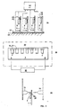
- a printed circuit board 1 is shown in plan view in FIG. 1A shown, which are equipped with memory modules 2 (e.g. eight) is.
- the circuit board 1 can be made of conventional FR-4 material consist.
- conductor tracks 3-9 have one Memory modules 2 connecting network, z.
- a data or Include address bus, capacitive load structures in the form printed conductor surfaces 16, one below the other and with one respective conductor track 3-9 through thin printed connecting lines 20 are connected.
- capacitive Load structures in the form of vias or Vias 18 can be provided, which are also individually thin printed connecting lines 21 with respective conductor tracks 3-9 are connected.
- the relevant can now be measured Delays or signal delays on the networks or Lines between those mounted on the printed circuit board 1
- Memory modules 2 selectively determined capacitive Load structures, d. H. individual conductor surfaces 16 and / or vias 18 are separated in order to avoid maximum signal delays to minimize.
- To separate the conductor surfaces 16 or the vias 18 become the thin connecting lines 20 or 21 cut by means of a cutting laser.
- the capacitive load structures shown in Figure 1B, i. H. the conductor surfaces 16 and / or the vias 18 can be so execute that their capacity to the respective chip package is in the femto or subfemtofarad range.
- FIGS. 2A, 2B and 2C schematically show one each Implementation of the method according to the invention Device and that in Figures 2A and 2B in elevation and in top view when measuring the delay times or the Signal propagation times on the networks, the individual integrated Circuits, e.g. B. memory modules 2 on a printed PCB 1 or on several printed circuit boards 1 connect with each other and in Figure 2C when severing capacitive load structures 16, 18.
- the individual integrated Circuits e.g. B. memory modules 2 on a printed PCB 1 or on several printed circuit boards 1 connect with each other and in Figure 2C when severing capacitive load structures 16, 18.
- FIG. 2A shows to be mounted on a motherboard 15, or the measurement 2B on a single circuit board 1 be carried out.
- the measuring means 12 are with sensors provided that a low-capacity, d. H. purely ohmic contact with the individual traces of an interested Establish line system or network, namely at the plug contact of the individual memory modules at the individual module level or motherboard level.
- Figures 2A and 2B also show holding means, e.g. B. a table 10 which is used to hold at least one printed Printed circuit board 1 is set up.
- holding means e.g. B. a table 10 which is used to hold at least one printed Printed circuit board 1 is set up.
- FIG. 2C shows that for carrying out the invention Process set up device when executing the Separation step, in which targeted by means of a cutting laser 14 individual connecting lines 20, 21 (Fig. 1B) on the printed circuit board 1 corresponding to that with an arrangement separated in accordance with FIGS. 2A, 2B become.
- FIG. 2C makes it clear that the disconnection of connecting lines from both sides of the circuit board from the laser 14 can be executed.
Landscapes
- Engineering & Computer Science (AREA)
- General Engineering & Computer Science (AREA)
- Physics & Mathematics (AREA)
- General Physics & Mathematics (AREA)
- Microelectronics & Electronic Packaging (AREA)
- Dram (AREA)
- Combinations Of Printed Boards (AREA)
- Structure Of Printed Boards (AREA)
- Design And Manufacture Of Integrated Circuits (AREA)
- Manufacturing Of Printed Wiring (AREA)
- Production Of Multi-Layered Print Wiring Board (AREA)
- Semiconductor Memories (AREA)
- Laser Beam Processing (AREA)
- Parts Printed On Printed Circuit Boards (AREA)
Abstract
Description
- Haltemittel zur Halterung wenigstens einer mit der bzw. den integrierten Schaltung(en) bestückten Leiterplatte, die mit kapazitiven Laststrukturen an wenigstens einem Leiterbahnzug eines Leitungssystems oder Netzes in der Nähe des oder der Gehäuse der integrierten Schaltung(en) versehen ist bzw. sind;
- Messmittel zur Messung relevanter Verzögerungs- bzw.
Signallaufzeiten auf den Netzen oder Leitungssystemen zwischen den integrierten Schaltungen auf der bzw. den Leiterplatte (n), und - Trennmittel zur selektiven Abtrennung bestimmter kapazitiver Laststrukturen so, dass durch die Messmittel gemessene maximale Signalverzögerungen minimiert werden.
Claims (12)
- Verfahren zur Anpassung/Abstimmung von Signallaufzeiten auf Leitungssystemen oder Netzen zwischen auf gedruckten Leiterplatten montierten integrierten Schaltungen, insbesondere schnellen Speicherbausteinen,
gekennzeichnet durch
folgende Schritte:A) Vorsehen von Leiterplatten mit kapazitiven Laststrukturen an wenigstens einem Leiterbahnzug des Leitungssystems oder Netzes in der Nähe des oder der Gehäuse der integrierten Schaltung(en);B) Messen aller relevanten Verzögerungs- bzw. Signallaufzeiten auf dem Netz oder dem Leitungssystem zwischen den integrierten Schaltungen;C) selektives Abtrennen von bestimmten kapazitiven Laststrukturen von dem wenigstens einen Leiterbahnzug gemäß dem Messergebnis in Schritt B, um auftretende maximale Signalverzögerungen zu minimieren. - Verfahren nach Anspruch 1,
dadurch gekennzeichnet,
dass die Schritte B und C wiederholt werden. - Verfahren nach Anspruch 1 oder 2,
dadurch gekennzeichnet,
dass die kapazitiven Laststrukturen in Schritt A jeweils eine Kapazität im Femto- oder Sub-Femtofaradbereich aufweisen. - Verfahren nach einem der vorangehenden Ansprüche,
dadurch gekennzeichnet,
dass der selektive Trennschritt C durch Laserschneiden ausgeführt wird. - Verwendung des Verfahrens nach einem der vorangehenden Ansprüche zur Signallaufzeitanpassung auf Leitungssystemen oder Netzen zwischen auf gedruckten Leiterplatten montierten schnellen DRAM-Speicherbausteinen.
- Verwendung nach Anspruch 5 bei nicht oder unterschiedlich abgestimmten Chips und Gehäusen.
- Verwendung nach Anspruch 5 oder 6 bei unterschiedlichen Materialien von DRAM-Bausteinen.
- Verwendung nach einem der Ansprüche 5-7 zum Ausgleich von Herstellungstoleranzen von gedruckten Leiterplatten und/oder Chipgehäusen.
- Vorrichtung zur Anpassung/Abstimmung von Signallaufzeiten auf Leitungssystemen oder Netzen zwischen auf gedruckten Leiterplatten montierten integrierten Schaltungen, insbesondere schnellen Speicherbausteinen,
dadurch gekennzeichnet,
dass die Vorrichtung in Kombination aufweist:Haltemittel (10) zur Halterung wenigstens einer mit der bzw. den integrierten Schaltung(en) (2) bestückten Leiterplatte (1), die mit kapazitiven Laststrukturen (16, 18) an wenigstens einem Leiterbahnzug (3-9) eines Leitungssystems oder Netzes in der Nähe des oder der Gehäuse der integrierten Schaltung(en) (2) versehen ist bzw. sind;Messmittel (12) zur Messung relevanter Verzögerungs-bzw. Signallaufzeiten auf den Netzen oder Leitungssystemen zwischen den integrierten Schaltungen auf der bzw. den Leiterplatte(n) (1), undTrennmittel (14) zur selektiven Abtrennung bestimmter kapazitiver Laststrukturen so, dass durch die Messmittel gemessene maximale Signalverzögerungen minimiert werden. - Vorrichtung nach Anspruch 9,
dadurch gekennzeichnet,
dass die kapazitiven Laststrukturen Flächen (16) und/oder Vias (18) aufweisen. - Vorrichtung nach Anspruch 9 oder 10,
dadurch gekennzeichnet,
dass die Trennmittel (14) einen Schneidelaser aufweisen. - Speicherbaugruppe mit einer gedruckten Leiterplatte und mindestens einem darauf montierten Speicherbaustein,
dadurch gekennzeichnet,
dass die gedruckte Leiterplatte (1) an wenigstens einer zu einem Signalübertragungsnetz oder -leitungssystem, das Signale zum/vom Speicherbaustein überträgt gehörenden Leiterbahn in der Nähe der Gehäuse-Footprintfläche des Speicherbausteins mit leicht abtrennbaren Leitungsstrukturen (16, 18), wie Flächen oder Vias versehen ist, die zur Leiterbahn und zu dem Gehäuse des montierten Speicherbausteins eine kapazitive Last bilden, wobei bestimmte der kapazitiven Laststrukturen an Leiterbahnen mit maximaler Signalverzögerung zur Minimierung gemessener maximaler Signallaufzeiten selektiv abtrennbar sind.
Applications Claiming Priority (2)
| Application Number | Priority Date | Filing Date | Title |
|---|---|---|---|
| DE10004649 | 2000-02-03 | ||
| DE10004649A DE10004649A1 (de) | 2000-02-03 | 2000-02-03 | Verfahren und Vorrichtung zur Anpassung/Abstimmung von Signallaufzeiten auf Leitungssystemen oder Netzen zwischen integrierten Schaltungen |
Publications (3)
| Publication Number | Publication Date |
|---|---|
| EP1130408A2 true EP1130408A2 (de) | 2001-09-05 |
| EP1130408A3 EP1130408A3 (de) | 2006-04-12 |
| EP1130408B1 EP1130408B1 (de) | 2007-06-27 |
Family
ID=7629640
Family Applications (1)
| Application Number | Title | Priority Date | Filing Date |
|---|---|---|---|
| EP01101831A Expired - Lifetime EP1130408B1 (de) | 2000-02-03 | 2001-01-26 | Verfahren und Vorrichtung zur Anpassung/Abstimmung von Signallaufzeiten auf Leitungssystemen oder Netzen zwischen integrierten Schaltungen |
Country Status (6)
| Country | Link |
|---|---|
| US (1) | US6968481B2 (de) |
| EP (1) | EP1130408B1 (de) |
| JP (1) | JP3415830B2 (de) |
| KR (1) | KR100438462B1 (de) |
| DE (2) | DE10004649A1 (de) |
| TW (1) | TW506029B (de) |
Families Citing this family (4)
| Publication number | Priority date | Publication date | Assignee | Title |
|---|---|---|---|---|
| US7902938B2 (en) | 2004-03-29 | 2011-03-08 | Nec Corporation | Data transmitter, data transmission line, and data transmission method |
| US7714629B2 (en) | 2007-05-29 | 2010-05-11 | Shinko Electric Industries Co., Ltd. | Delay circuit and delay time adjustment method |
| JP6320231B2 (ja) | 2014-08-04 | 2018-05-09 | 株式会社ワコム | 位置指示器及びその製造方法 |
| TWI796549B (zh) | 2020-02-26 | 2023-03-21 | 頎邦科技股份有限公司 | 線路板 |
Family Cites Families (11)
| Publication number | Priority date | Publication date | Assignee | Title |
|---|---|---|---|---|
| JPS5694800A (en) * | 1979-12-28 | 1981-07-31 | Taiyo Yuden Kk | Method and device for mounting electronic part |
| DE3301673A1 (de) * | 1983-01-20 | 1984-07-26 | Brown, Boveri & Cie Ag, 6800 Mannheim | Elektrisches bzw. elektronisches mehrschichtbauelement |
| US4641112A (en) * | 1985-03-12 | 1987-02-03 | Toko, Inc. | Delay line device and method of making same |
| FI78577C (fi) * | 1987-12-30 | 1989-08-10 | Vaisala Oy | Foerfarande foer avstaemning av en plankondensator. |
| US4876702A (en) * | 1988-07-28 | 1989-10-24 | Hewlett-Packard Company | Programmable time advance |
| US5329237A (en) * | 1993-02-12 | 1994-07-12 | Micron Semiconductor, Inc. | Method and system for decoupling inoperative passive elements on a semiconductor chip |
| US5578930A (en) * | 1995-03-16 | 1996-11-26 | Teradyne, Inc. | Manufacturing defect analyzer with improved fault coverage |
| US5796746A (en) * | 1995-12-22 | 1998-08-18 | Micron Technology, Inc. | Device and method for testing integrated circuit dice in an integrated circuit module |
| GB2314699A (en) * | 1996-06-27 | 1998-01-07 | Motorola Ltd | Detecting overheating of printed circuit boards |
| DE19825607C2 (de) * | 1998-06-08 | 2000-08-10 | Siemens Ag | Integrierte Halbleiterschaltung mit Füllstrukturen |
| US6223334B1 (en) * | 1998-10-01 | 2001-04-24 | Mentor Graphics Corporation | Automatic topology synthesis and optimization |
-
2000
- 2000-02-03 DE DE10004649A patent/DE10004649A1/de not_active Withdrawn
-
2001
- 2001-01-26 DE DE50112651T patent/DE50112651D1/de not_active Expired - Lifetime
- 2001-01-26 EP EP01101831A patent/EP1130408B1/de not_active Expired - Lifetime
- 2001-02-01 JP JP2001025715A patent/JP3415830B2/ja not_active Expired - Fee Related
- 2001-02-01 TW TW090102011A patent/TW506029B/zh not_active IP Right Cessation
- 2001-02-02 KR KR10-2001-0005077A patent/KR100438462B1/ko not_active Expired - Fee Related
- 2001-02-05 US US09/776,951 patent/US6968481B2/en not_active Expired - Fee Related
Also Published As
| Publication number | Publication date |
|---|---|
| DE50112651D1 (de) | 2007-08-09 |
| JP2001251030A (ja) | 2001-09-14 |
| EP1130408A3 (de) | 2006-04-12 |
| KR100438462B1 (ko) | 2004-07-03 |
| TW506029B (en) | 2002-10-11 |
| US20010031507A1 (en) | 2001-10-18 |
| US6968481B2 (en) | 2005-11-22 |
| KR20010078290A (ko) | 2001-08-20 |
| EP1130408B1 (de) | 2007-06-27 |
| JP3415830B2 (ja) | 2003-06-09 |
| DE10004649A1 (de) | 2001-08-09 |
Similar Documents
| Publication | Publication Date | Title |
|---|---|---|
| DE60208579T2 (de) | Mehrchip-verbindungssystem | |
| DE19827237B4 (de) | Leiterplattensubstrat für Halbleiterbauelementgehäuse und ein dasselbe verwendende Halbleiterbauelementgehäuse sowie Herstellungsverfahren für diese | |
| DE10160041A1 (de) | Elektronisches Schaltungsmodul und Verfahren zu dessen Montage | |
| EP0351581A1 (de) | Hochintegrierte Schaltung sowie Verfahren zu deren Herstellung | |
| DE69208415T2 (de) | Direkte Verteilerreparatur und System einer technischen Veränderung | |
| EP1602263B1 (de) | Verfahren zum hf-abstimmen einer elektrischen anordnung sowie eine hierzu geeignete leiterplatte | |
| DE102005060930A1 (de) | Speicheranwendungstester mit vertikal montierter Hauptplatine | |
| DE112006000862T5 (de) | Induktor | |
| DE112017007145T5 (de) | Zwischenplattenverbindungsstruktur | |
| EP1130408A2 (de) | Verfahren und Vorrichtung zur Anpassung/Abstimmung von Signallaufzeiten auf Leitungssystemen oder Netzen zwischen integrierten Schaltungen | |
| EP0007993A1 (de) | Leiterplatte zur Halterung und elektrischen Verbindung von Halbleiterchips | |
| DE2753236C2 (de) | Einbaurahmen für eine gehäuselose integrierte Halbleiterschaltungsanordnung | |
| DE102004041961B3 (de) | Integrierte Halbleiterschaltung mit integrierter Kapazität zwischen Kontaktanscluss und Substrat und Verfahren zu ihrer Herstellung | |
| DE29622830U1 (de) | Leiterplattennutzen | |
| DE4038460A1 (de) | Smd-bauteilverbindung zu einer leiterplatte | |
| DE10308926B4 (de) | Halbleiterchipanordnung und Verfahren zu ihrer Herstellung | |
| EP2166825A1 (de) | Lötbares elektronisches Modul mit Schaltungsträger | |
| DE102020116233A1 (de) | Schaltungsträger mit Anschlussflächenfeld und Verfahren zum Herstellen eines Anschlussflächenfelds auf einem Schaltungsträger | |
| EP3886160A1 (de) | Hochfrequenzanordnung mit zwei miteinander verbundenen hochfrequenzkomponenten | |
| DE19749663A1 (de) | Halbleiterbauelement-Testgerät | |
| DE10131940B4 (de) | Halbleiterchip und Verfahren zur Ausbildung von Kontakten auf einer Halbleiteranordnung | |
| DE2629303B2 (de) | Mehrschichtleiterplatte und Verfahren zu ihrer Herstellung | |
| WO2018149575A1 (de) | Leiterplatte mit gestapelten bauelementen und verfahren zur deren herstellung | |
| DE102004009337A1 (de) | Kontaktplatte zur Verwendung bei einer Kalibrierung von Testerkanälen eines Testersystems sowie ein Kalibriersystem mit einer solchen Kontaktplatte | |
| DE10203151C1 (de) | Vorrichtung zum Anschließen von Halbleitermodulen, insbesondere Speicherbänken |
Legal Events
| Date | Code | Title | Description |
|---|---|---|---|
| PUAI | Public reference made under article 153(3) epc to a published international application that has entered the european phase |
Free format text: ORIGINAL CODE: 0009012 |
|
| AK | Designated contracting states |
Kind code of ref document: A2 Designated state(s): AT BE CH CY DE DK ES FI FR GB GR IE IT LI LU MC NL PT SE TR |
|
| AX | Request for extension of the european patent |
Free format text: AL;LT;LV;MK;RO;SI |
|
| PUAL | Search report despatched |
Free format text: ORIGINAL CODE: 0009013 |
|
| AK | Designated contracting states |
Kind code of ref document: A3 Designated state(s): AT BE CH CY DE DK ES FI FR GB GR IE IT LI LU MC NL PT SE TR |
|
| AX | Request for extension of the european patent |
Extension state: AL LT LV MK RO SI |
|
| RIC1 | Information provided on ipc code assigned before grant |
Ipc: H01L 21/66 20060101ALI20060220BHEP Ipc: G01R 31/317 20060101AFI20010717BHEP |
|
| RAP1 | Party data changed (applicant data changed or rights of an application transferred) |
Owner name: QIMONDA AG |
|
| 17P | Request for examination filed |
Effective date: 20061006 |
|
| AKX | Designation fees paid |
Designated state(s): DE |
|
| GRAP | Despatch of communication of intention to grant a patent |
Free format text: ORIGINAL CODE: EPIDOSNIGR1 |
|
| GRAS | Grant fee paid |
Free format text: ORIGINAL CODE: EPIDOSNIGR3 |
|
| GRAA | (expected) grant |
Free format text: ORIGINAL CODE: 0009210 |
|
| AK | Designated contracting states |
Kind code of ref document: B1 Designated state(s): DE |
|
| REF | Corresponds to: |
Ref document number: 50112651 Country of ref document: DE Date of ref document: 20070809 Kind code of ref document: P |
|
| PLBE | No opposition filed within time limit |
Free format text: ORIGINAL CODE: 0009261 |
|
| STAA | Information on the status of an ep patent application or granted ep patent |
Free format text: STATUS: NO OPPOSITION FILED WITHIN TIME LIMIT |
|
| 26N | No opposition filed |
Effective date: 20080328 |
|
| PGFP | Annual fee paid to national office [announced via postgrant information from national office to epo] |
Ref country code: DE Payment date: 20150305 Year of fee payment: 15 |
|
| REG | Reference to a national code |
Ref country code: DE Ref legal event code: R081 Ref document number: 50112651 Country of ref document: DE Owner name: INFINEON TECHNOLOGIES AG, DE Free format text: FORMER OWNER: QIMONDA AG, 81739 MUENCHEN, DE Ref country code: DE Ref legal event code: R081 Ref document number: 50112651 Country of ref document: DE Owner name: POLARIS INNOVATIONS LTD., IE Free format text: FORMER OWNER: QIMONDA AG, 81739 MUENCHEN, DE |
|
| REG | Reference to a national code |
Ref country code: DE Ref legal event code: R081 Ref document number: 50112651 Country of ref document: DE Owner name: POLARIS INNOVATIONS LTD., IE Free format text: FORMER OWNER: INFINEON TECHNOLOGIES AG, 85579 NEUBIBERG, DE |
|
| REG | Reference to a national code |
Ref country code: DE Ref legal event code: R119 Ref document number: 50112651 Country of ref document: DE |
|
| PG25 | Lapsed in a contracting state [announced via postgrant information from national office to epo] |
Ref country code: DE Free format text: LAPSE BECAUSE OF NON-PAYMENT OF DUE FEES Effective date: 20160802 |