EP1129580B1 - Taktrückgewinnung - Google Patents
Taktrückgewinnung Download PDFInfo
- Publication number
- EP1129580B1 EP1129580B1 EP00964166A EP00964166A EP1129580B1 EP 1129580 B1 EP1129580 B1 EP 1129580B1 EP 00964166 A EP00964166 A EP 00964166A EP 00964166 A EP00964166 A EP 00964166A EP 1129580 B1 EP1129580 B1 EP 1129580B1
- Authority
- EP
- European Patent Office
- Prior art keywords
- frequency
- clock
- clock frequency
- divider
- ref
- Prior art date
- Legal status (The legal status is an assumption and is not a legal conclusion. Google has not performed a legal analysis and makes no representation as to the accuracy of the status listed.)
- Expired - Lifetime
Links
Images


Classifications
-
- H—ELECTRICITY
- H04—ELECTRIC COMMUNICATION TECHNIQUE
- H04L—TRANSMISSION OF DIGITAL INFORMATION, e.g. TELEGRAPHIC COMMUNICATION
- H04L7/00—Arrangements for synchronising receiver with transmitter
-
- H—ELECTRICITY
- H04—ELECTRIC COMMUNICATION TECHNIQUE
- H04N—PICTORIAL COMMUNICATION, e.g. TELEVISION
- H04N21/00—Selective content distribution, e.g. interactive television or video on demand [VOD]
- H04N21/40—Client devices specifically adapted for the reception of or interaction with content, e.g. set-top-box [STB]; Operations thereof
- H04N21/43—Processing of content or additional data, e.g. demultiplexing additional data from a digital video stream; Elementary client operations, e.g. monitoring of home network or synchronising decoder's clock; Client middleware
- H04N21/4302—Content synchronisation processes, e.g. decoder synchronisation
- H04N21/4305—Synchronising client clock from received content stream, e.g. locking decoder clock with encoder clock, extraction of the PCR packets
-
- H—ELECTRICITY
- H03—ELECTRONIC CIRCUITRY
- H03L—AUTOMATIC CONTROL, STARTING, SYNCHRONISATION, OR STABILISATION OF GENERATORS OF ELECTRONIC OSCILLATIONS OR PULSES
- H03L7/00—Automatic control of frequency or phase; Synchronisation
- H03L7/06—Automatic control of frequency or phase; Synchronisation using a reference signal applied to a frequency- or phase-locked loop
- H03L7/16—Indirect frequency synthesis, i.e. generating a desired one of a number of predetermined frequencies using a frequency- or phase-locked loop
- H03L7/18—Indirect frequency synthesis, i.e. generating a desired one of a number of predetermined frequencies using a frequency- or phase-locked loop using a frequency divider or counter in the loop
- H03L7/1806—Indirect frequency synthesis, i.e. generating a desired one of a number of predetermined frequencies using a frequency- or phase-locked loop using a frequency divider or counter in the loop the frequency divider comprising a phase accumulator generating the frequency divided signal
-
- H—ELECTRICITY
- H04—ELECTRIC COMMUNICATION TECHNIQUE
- H04J—MULTIPLEX COMMUNICATION
- H04J3/00—Time-division multiplex systems
- H04J3/02—Details
- H04J3/06—Synchronising arrangements
- H04J3/062—Synchronisation of signals having the same nominal but fluctuating bit rates, e.g. using buffers
- H04J3/0632—Synchronisation of packets and cells, e.g. transmission of voice via a packet network, circuit emulation service [CES]
Definitions
- the invention relates to a device for processing a data stream, the device comprising a clock recovery system for locking a clock frequency to a time base of the data stream by comparing the clock frequency to time stamps representing the time base.
- the invention further relates to a method of locking a clock frequency to a time base of a data stream by comparing the clock frequency to time stamps representing the time base.
- US-A 5,699,392 discloses a system for the recovery of an encoder clock from an MPEG-2 transport stream.
- the frequency of a decoder clock is maintained at approximately the same frequency as an encoder clock, based on program clock reference (PCR) values contained in a digital information stream.
- a voltage-controlled oscillator produces a decoder clock frequency of 27 MHz.
- the decoder clock is fed back to a counter to produce a local system time clock (STC).
- STC system time clock
- the counter is initially loaded with a PCR value from the digital data stream.
- a subtractor subtracts the value of the PCR from the value of the local STC to produce an error signal.
- the error signal is filtered, scaled, and added to a control variable within a lowpass filter and processor.
- the control signal is applied to the voltage-controlled oscillator to adjust the oscillation frequency of the oscillator.
- Document US 5,767,746 A relates to a method and an apparatus for adjusting phase lock loop, PLL, parameters. More particularly it teaches to adjust the gain of a PLL in a decoder depending on the evaluated time information, like the program clock reference, PCR, sent by the encoder.
- the decoder comprises a video decoder section, an audio decoder section, and a clock control for synchronizing the video decoder section and the audio decoder section.
- the clock control includes a PLL control which calculates the PCR for adjusting a VCO. At first, the PCR measured by the clock reference, CR, measure is used to initialize a counter. Then the next PCR is used to determine whether the clock frequency needs to be adjusted.
- the difference between the current value and the value of the counter is determined by a difference section.
- the obtained delta is forwarded to a gain section.
- a gain factor A is multiplied to the delta time for reducing the effect of a particular measured delta time.
- the previous value which is multiplied with a gain factor 1- A is added to the current value.
- VCO voltage control oscillator
- Document JP 10 136259 A relates to an audio/video/computer graphics data synchronous reproducing/synthesizing system.
- a demultiplexer separates a received signal into audio packets, video packets, computer graphic packets and SCR/PCR packets.
- the SCR/PCR is used to control the oscillation frequency. More particularly, not the system clock of the system but the decoding clock generated by the video PLL is used as reference time.
- the MPEG standards provide for the transmission of digital information from multiple sources by dividing the digital data into a number of packets. The packets are then multiplexed onto a single data channel, allowing a relatively large number of users to transmit and receive data over a common data channel. All audio, video and auxiliary information to be carried within a given data channel is divided into 188-byte long transport packets. Each transport packet is subdivided into a header and a payload. The header carries information to identify the type of data that is carried within the payload and information required for decoding the transport packet stream.
- the PCR is a 42-bit value that represents time stamps from a relative STC that is clocked by an encoder clock within an MPEG-2 encoder.
- the first 33 bits of the PCR value are referred to as the PCR base, and express a value of the encoder system time clock in 90 kHz time base units.
- the remaining 9 bits of the PCR value are referred to as the PCR extension, and express a value of the system time clock in 27 MHz (modulo 300) time base units.
- the MPEG-2 standard requires that the PCR values must be provided at intervals of no more than 100 ms in the transport stream. The PCR values within the MPEG-2 transport stream are used to accurately recover the encoder clock in the MPEG-2 decoder.
- the transport stream is provided with presentation time-stamps (PTS) to indicate to the MPEG-2 decoder when to present the individual frames of video and audio data to the user.
- PTS presentation time-stamps
- the value of each PTS is ultimately dictated by the frequency of the encoder clock in the encoder, which clocks an STC in the MPEG-2 encoder.
- the MPEG-2 encoder inserts the PTS into the transport stream based on samples of the STC.
- the decoder clock in the MPEG-2 decoder must therefore operate at the same frequency as the encoder clock if the data streams are to be properly presented to a user.
- "synchronization" between the encoder clock and the decoder clock implies that the clocks are operating at the same frequency, but with a possible phase offset between them.
- synchronizing the encoder and the decoder clocks eliminates frame skips or frame holds that occur when displaying the transmitted data.
- a frame skip can occur when data is received later than its PTS denotes.
- a frame hold can occur when the buffer within the decoder receives insufficient audio or video data to perform the decoding.
- a phase locked loop is provided in the clock recovery system.
- the voltage-controlled oscillator operates at a nominal oscillation frequency of 27 MHz and has a control input to adjust the frequency within a small range surrounding the 27 MHz nominal frequency.
- the decoder clock is used for demultiplexing, decoding and displaying the audio and video.
- An object of the invention is, inter alia, to provide a more flexible and cost-effective clock recovery system.
- the invention provides a data processing device and a method of locking a clock frequency to a time base of a data stream as defined in the independent claims.
- Advantageous embodiments are defined in the dependent claims.
- a first embodiment of the invention is characterized in that said clock recovery system comprises: a free running clock for generating a free running reference frequency; and means for synthesizing said clock frequency from said reference frequency under control of said time stamps.
- a free running clock is more cost-effective than a de-tunable crystal as is used in embodiments that are known from the prior art. Faster locking and a larger tracking range can be achieved.
- the invention further offers more flexibility in choosing another frequency.
- An embodiment of the invention comprises further means for synthesizing a further clock frequency from said reference frequency without locking to said time base.
- a further clock frequency for which locking to the time base of the incoming data stream is not necessary, is generated from the free running reference frequency, for example by a dedicated phase locked loop.
- This embodiment provides a clock system that provides locked clocks as well as unlocked clocks.
- the free running reference frequency is used for both types of clocks as a reference clock. Locking is only performed for those clocks that really need locking, e.g. clocks for use in MPEG audio and video processing units.
- said further means comprise a multiplier for multiplying said reference frequency by an appropriate integer number to obtain said further clock frequency.
- said synthesizing means comprise a controlled multiplier for multiplying the reference frequency by an appropriate number to obtain said clock frequency, said appropriate number being derived under control of said time stamps.
- the appropriate number is made controllable by a processing unit. Locking to the time base of the incoming data stream is achieved by comparing the locked clock frequency with the incoming time stamps and to calculate the appropriate number by the processing unit.
- the controlled multiplier comprises a phase locked loop (PLL) circuit for obtaining an oscillation frequency at an integer multiple of the reference frequency, said circuit comprising a phase detector coupled to an oscillator, and a feedback loop for feeding the oscillation frequency to an input of the phase detector, said feedback loop comprising an integer divider; and a controlled divider for dividing the oscillation frequency by a non-integer divider number to obtain a divided frequency, said divider number being derived under control of said time stamps and said divided frequency being output as the clock frequency.
- PLL phase locked loop
- said controlled multiplier comprises: a phase locked loop circuit for obtaining an oscillation frequency at an integer multiple of the reference frequency, said circuit comprising a phase detector coupled to an oscillator; a controlled divider for dividing the oscillation frequency by a non-integer divider number to obtain a divided frequency, said divider number being derived under control of said time stamps; a counter for counting the number of positive edges in the divided frequency per cycle of the reference frequency; means for generating a predetermined frequency comprising an amount of positive edges at predetermined positions, said amount being equal to said number of positive edges in the divided frequency and said predetermined frequency being output as the clock frequency; and a feedback loop for feeding the clock frequency to an input of the phase detector, said feedback loop comprising an cascaded divider being arranged to divide the clock frequency by a divider number equal to said number of positive edges.
- An advantageous embodiment of the invention comprises means for synthesizing clock frequencies for audio processing and video processing independently. Locking the audio and video clocks independently has the additional advantage that even PTS time stamps can be involved in the regulation by which an exact time base match can be achieved. Also time base discontinuities can be optimized independently.
- a further embodiment comprises first processing means for performing a first processing step with use of said clock frequency; second processing means for performing a second processing step with use of said further clock frequency; and a sample rate converter for converting a sample rate of an output signal of the first processing means to furnish converted output signals to the second processing means.
- This embodiment provides a solution for coupling a unit that runs on a locked clock frequency and a second unit that runs on an unlocked, i.e. a different frequency.
- the sample rate converters compensate for the clock jitter, so that no difficult high performance analog PLL's are required.
- This embodiment is especially useful for running audio and video processing units on a locked clock frequency and digital to analog converters coupled to the processing units on an unlocked clock frequency.
- the D/A converter for the video part runs at an integer multiple of the clock frequency of the audio D/A converter. This integer can be equal to one, so that the audio and video D/A converters run at the same clock frequency.
- the sample rate converter may be controlled by phase information out of the controlled multiplier.
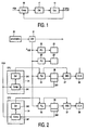
- the clock recovery system of Fig. 1 schematically shows a system as is known from the prior art.
- This system comprises a comparator 10, a control unit 11 and an oscillator 12.
- the oscillator is controllable by the control unit 11.
- the output of the oscillator is about 27 MHz, which is fed back to the comparator 10.
- the output frequency of 27 MHz is de-tunable within a small range of approximately 100 ppm.
- the comparator 10 compares the clock frequency with the incoming time stamps PCR. Based on the comparison performed in the comparator; the frequency of the oscillator is adjusted.
- the 27 MHz frequency is used as a clock frequency in the decoder.
- the conventional 27 MHz is only optimized for standard ITU656 based video.
- FIG. 2 A data processing device according to the invention is shown in Fig. 2 .
- the invention is applicable to any data stream comprising time stamps, the following discussion will concentrate on an MPEG encoded data stream.
- the device comprises a free running clock 20 that produces an exemplary free running frequency of 24.576 MHz. This is a practical frequency for a DVB set top box. Dependent on the specific application another frequency might be more practical. A practical frequency for a TV is e.g. 24.0 MHz.
- a frequency divider 21 is an optional element that can be used to divide the frequency of the free running clock 20.
- the frequency divider 21 can be part of the free running clock and may also be omitted.
- the frequency divider 21 is assumed to be present and to divide the frequency of the free running clock 20 by 4 to obtain a free running reference frequency F REF of 6.144 MHz. This single low reference frequency F REF is distributed over the device.
- the free running frequency generated by the free running clock 20 or a derivative thereof, is optionally output to an external device or communication bus, for example external SDRAM, an IEEE1394 interface or a modem. If the divider 21 is omitted, the reference frequency F REF is equal to the frequency as generated by the free running clock 20.
- the device comprises PLL's 22 and 22', which generate local frequencies for the sub-system units 23 and 23' respectively.
- the units 23 and 23' perform some processing function. Examples of sub-system units 23 and 23' are, among others: memory interfaces, central processing units (CPU's), peripherals, decoders, etc.
- Time stamps PCR represent a time base of an incoming data stream.
- a clock that needs locking to the time base is synthesized from the reference frequency F REF under control of the time stamps PCR.
- MPEG presentation units for example, need clock frequencies that are locked to the time base of the incoming data stream.
- the device For locking an MPEG video processing clock frequency to the time stamps PCR, the device comprises a CPU 24 and a controlled multiplier 25 (PLL). Locking to the time base of the incoming data stream is achieved by comparing the video time base, i.e. the video processing clock frequency with the incoming time stamps PCR and to calculate an appropriate multiplying factor by the CPU 24.
- the CPU 24 calculates appropriate divider numbers for non-integer dividers that are used in the PLL that forms the controlled multiplier 25 as will be discussed in relation to Fig. 3 .
- the CPU 24 comprises a compare unit 241 and a control unit 240.
- the video processing clock frequency is output from the PLL 25 to a video processing unit 26.
- Coupled to the video-processing unit 26 is a video time counter 261.
- the video time counter 261 is used to divide and feed back the required video time base to the compare unit 241 in the CPU 24.
- the audio part of the device is implemented in a similar way and comprises a CPU 34 comprising a compare unit 341 and a control unit 340.
- the audio part further comprises a controlled multiplier 35 (PLL) and an audio processing unit 36 coupled to an audio time counter 361.
- PLL controlled multiplier 35
- the elements in the audio part are similar to their counterpart in the video part of the device.
- time base regulation for the audio and video parts of the device independently, has the additional advantage that time base discontinuities can be optimized individually. Furthermore, decoding and presentation time stamps can be involved in the regulation so that an exact time base match can be achieved.
- MPEG-2 decoding and presentation time stamps are described in US-A 5,652,627 .
- a presentation time stamp (PTS) specifies the time at which each picture is to be displayed, and a decode time stamp (DTS) specifies the time at which a picture is to be decoded when the decoding time differs from the presentation time.
- PTS presentation time stamp
- DTS decode time stamp
- Each MPEG-2 picture and audio frame is tagged (explicitly or implicitly) with a DTS, which indicates the time of the decoder clock at which the picture or audio frame should be decoded.
- a DTS for a particular picture or audio frame is not explicitly coded in the MPEG-2 bit stream, then that picture or audio frame is decoded immediately following the previous one. Both pictures and audio frames are transmitted in order of increasing DTS value. Because MPEG-2 requires some pictures to be transmitted several pictures earlier in sequence than they are to be shown (i.e. prior to a B-picture), these pictures also require a second time stamp called the presentation time stamp (PTS) which indicates the clock value at which the picture is intended to be shown. If only a single time stamp is coded (as is always the case with audio), it is assumed to be both the DTS and PTS. Beginning both the video and audio at the time indicated in their respective PTS fields ensures synchronization (lip sync) of the audio and video. Locking to DTS can be done in a similar way as locking PTS.
- PTS presentation time stamp
- a practical frequency for the video part is 27 MHz.
- Practical frequencies for the audio part are 24.6 or 22.6 MHz, i.e. a multiple of the audio sampling frequency.
- the clock system of Fig. 2 provides locked and unlocked clocks with crystal stability.
- video and audio digital to analog (D/A) converters 28 and 38 run on a frequency that is derived from the free running reference frequency F REF without locking to the time base of the incoming data stream.
- PLL's similar to the PLL's 22 and 22' are used. It is however also possible to derive the clock frequencies for the D/A converters 28 and 38 in an alternative way. For integration on a single Integrated Circuit (IC) it is profitable to run the D/A converters 28, 38 on a simple mutual clock ratio or on the same clock frequency, e.g. running the video D/A converter 28 on an integer multiple of the audio D/A converter 38 clock frequency.
- IC Integrated Circuit
- Fig. 3 shows a generalized block diagram of PLL clock synthesizing according to the invention.
- a PLL is a closed loop frequency control system which functioning is based on phase sensitive detection of phase difference between an input signal and an output signal of a controlled oscillator.
- the PLL controls the oscillator so that it maintains a constant phase angle relative to a reference signal.
- Fig. 3 shows the PLL 22, which does not lock the clock frequency to the time base of the incoming data stream and the PLL 25 that generates the video presentation clock, which is locked to the time base of the incoming data stream.
- the PLL 22' and the PLL 35 are similar to the PLL 22 and the PLL 25, respectively.
- the PLL 22 comprises a phase detector 221 (PD), a loop filter 222 (LPF), a controlled oscillator 223 (Osc), a first divider 224 (DivN1), and a second divider 225 (DivN2) being placed in a feedback loop.
- the unlocked further clock frequencies that are used in the sub-systems are integer multiples of the free running reference frequency F REF .
- the dividers 224, 225 are therefore simple, integer dividers.
- the oscillator 223 generates a frequency that is an integer multiple of the reference frequency F REF .
- the frequency of the oscillator 223 is thereafter divided in the first divider 224 by an integer number N1 to generate the further clock frequency F OUT (1) that is used in the sub-system 23.
- the further clock frequency F OUT (1) is fed back to the phase detector 221 after dividing by a second integer number N2 in the second divider 225 to make comparison with the reference frequency F REF possible. This is necessary because the further clock frequency F OUT (1) is an integer multiple of the reference frequency F REF .
- the generated frequency of the controlled oscillator 223 is amended by use of the loop filter 222 to keep a constant phase angle between the further clock frequency F OUT (1) and the reference frequency F REF .
- the PLL 25 comprises a phase detector 251, a loop filter 252, an oscillator 253, a first divider 254 (DivM1) and a second divider 255 (DivM2).
- the free running reference frequency F REF is used as a reference.
- the divider 254 is a non-integer divider dividing by a non-integer divider number M1.
- the non-integer divider number M1 is made controllable by the CPU 24.
- the non-integer divider 254 can be implemented as shown in Fig 4A .
- the non-integer divider 254 comprises an accumulator 256 and a feedback register 257. Such a divider is also called a discrete time oscillator or a numerically controlled oscillator.
- the register 257 receives the frequency F OSC that has been generated by the oscillator 253. In an exemplary embodiment, F OSC is 73.728 MHz having a width of 22 bits.
- the divider 254 divides the oscillation frequency to the desired locked frequency of 27 MHz.
- the most significant bit msb, of the 23-bit output of the register 257 represents the output frequency F OUT .
- the remaining 22-bit output of the register 257 is fed back to the accumulator 256.
- the accumulator 256 further receives a 22-bit number m that is obtained from the CPU 24.
- the feedback signal and the number m are accumulated in the accumulator 256 and thereafter transmitted as a 23-bit number to the register 257.
- Four is equal to m times 73,728,000/2 22 , i.e. m times 17.6 Hz.
- F OUT 27.0 MHz
- the number m should be 1,536,000.
- This number m is calculated in the CPU under control of the time stamps PCR as described above and represents the divider-number M1.
- the regulation accuracy of the illustrated 22-bit implementation is 0.65 ppm (17.6 / 27,000,000). If a higher accuracy for the output frequency F OUT is required, the data path in the feedback loop has to be widened by one bit for every factor 2. It should be noted that the data in the feedback loop represents the phase relation phs between F OUT and Fosc.
- FIG. 5 shows a practical implementation of a locked clock generator with a non-integer divider 254.
- the frequency F OUT (P) is locked to the MPEG time base via the CPU controlled divider 254.
- the oscillation frequency F OSC is fed back to the phase detector 251 via a divider 255 * rather than the output frequency F OUT .
- An advantage of this embodiment is that the divider 255* can be implemented as a simple integer divider, because F OSC is an integer multiple of F REF . Due to the unknown load in an MPEG clock tree, the delay d of the divider 254, i.e. the relation with F REF is lost. In this embodiment, clock skew and clock jitter are not minimized.
- solutions are proposed to minimize clock jitter and clock skew.
- Clock jitter in the embodiment of Fig. 5 can be reduced by increasing the oscillation frequency F OSC , e.g. by a factor 4 to 294.9 MHz.
- An advantage thereof is that the design of the digital part is simplified.
- a disadvantage is that the clock requirements for the D/A converter 28 might not be satisfied. Also post-PLL's as in the existing implementation for audio will have their limitation in signal quality.
- Fig. 6 shows an embodiment for compensating clock jitter in an advantageous manner.
- the D/A converter 28 runs on a frequency that is derived from the reference frequency F REF without locking to the MPEG time base, which frequency has a low jitter.
- the D/A converter 28 runs on F OSC which is in fact an unlocked integer multiple of the reference frequency F REF .
- the feedback in the PLL is performed by the divider 255*, in the same way as already discussed in relation to Fig. 5 .
- a sample rate converter 27 (SRC) is used in the signal path for converting the sample rate of the output signal of the video-processing unit 26 to furnish a converted video stream to the D/A converter 28.
- SRC sample rate converter 27
- the D/A converter 28 runs on a different frequency than the video-processing unit 26 that runs on the locked clock frequency F OUT (P).
- F OUT locked clock frequency
- any processing unit which runs on an unlocked frequency and is coupled to another unit that runs on a locked frequency, could be used with a sample rate converter to convert the sample rate of the signal.
- the sample rate converter 27 can be controlled by phase information phs out of the non-integer divider 254.
- the additional advantage is that the audio and video D/A converters 28, 38 can run on the same clock frequency or on different clock frequencies having a simple mutual ratio, e.g. an integer number, which simplifies the integration of both converters on the same chip significantly.
- Reduction of clock skew can be achieved by introducing a feedback loop from F OUT (P) to F REF as shown in Fig. 7A .
- F OUT P
- F REF F REF
- Fig. 7A This is in conformity with the non-integer PLLs as shown in Fig. 3 .
- the main difference between the embodiments shown in Figs. 5 and 7A is that the divider 255 in the feedback loop as shown in Fig. 7A needs to be a non-integer divider, instead of a integer divider.
- the divider 255 can be implemented similar to the non-integer divider 254.
- a timing diagram of the embodiment of Fig. 7A is shown in Fig. 7B .
- the non-integer divider number M2 is equal to 4.39 (27.0 / 6.144).
- F OUT exhibits in this embodiment clock jitter with reference to F REF . Additional measures are proposed to minimize this clock jitter.
- FIG. 8a An illustration of an embodiment comprising these additional measures is shown in Fig. 8a .
- the non-integer divider 254 is the same as described above. This divider converts the Fosc of 72.728 MHz to F OUT (P), being 27.0 MHz and locked to the MPEG time base. The number of positive edges in each F REF cycle T REF is counted in edge counter 259. For F OSC is 72.728 MHz and F OUT (P) is 27.0 MHz, the number of positive edges will be 4 or 5, because 27.0 / 6.144 is 4.73.
- the edge counter 259 uses F OSC being divided by 12 in divider 258 as representation of F REF . The output of the edge counter 259 is the number of counted positive edges, being 4 or 5 in this implementation.
- F OUT (P) is generated with exactly the same number of positive edges for a F REF cycle, but at predetermined positions.
- the embodiment therefore comprises a selector 260 that selects a predetermined sequence 4Fx or 5Fx, depending on the number of positive edges counted for output, as F OUT (P).
- the divider 255 is being arranged as a cascaded divider, bringing down F OUT (P) to 6.144 MHz by switching between two integer numbers depending on the counted number of positive edges as provided by the edge counter.
- the resulting frequency F X has the proper frequency and no jitter compared to F REF .
- the frequency F X can therefore be used in the phase detector.
- the phase relation between F OUT and F REF is only determined by the delay of the divider 255. In this way, independence of clock tree load is achieved, resulting in a minimized clock skew with other domains, even with clock frequencies that have integer relationships with F REF .
- the invention thus provides clocks that have crystal stability, exhibit low clock skew and are controllable over a large frequency range.
- the same mechanism can be used for the generation of the clock frequency for the audio part, where the clock frequency is either 24.6 or 22.6 MHz. Also here the number of clocks per reference clock cycle T REF is between 4 and 5. Only the switching will occur at a different ratio in order to achieve the proper output frequency value.
- the mechanism of clock edge permutation is only effective in the digital domain and does not change the average frequency.
- the sample rate converters 27, 37 in front of the D/A converters 28, 38 do not require any modification, although required buffering may need to be enlarged by one sample.
- the invention relates to a data processing device having a clock recovery system for locking a clock frequency to time stamps of an incoming data stream, e.g. MPEG. It has been proposed to use a free running clock that generates a reference frequency from which a desired locked clock frequency is synthesized under control of a processing unit that compares the locked clock frequency to the time stamps.
- the invention provides a cost-effective and flexible system.
- MPEG audio and video processing clock frequencies are synthesized from a free running reference frequency and locked to the MPEG time base on basis of time stamps provided in the MPEG data stream.
- Other sub-systems run on clock frequencies that are not locked to the time base, e.g. simple multiples of the free running reference frequency.
- Audio and video D/A converters run on the same clock frequency or on two different clock frequencies having a simple mutual ratio that are synthesized from the free running reference frequency without locking to the time base.
- Sample rate converters are present in the signal path to adjust the output signal of a processing unit to the input of the D/A converter. Time base regulation for audio and video is performed independently.
Claims (12)
- Vorrichtung zum Verarbeiten eines Datenstroms, wobei die Vorrichtung ein Taktrückgewinnungssystem zum Synchronisieren einer Taktfrequenz auf eine Zeitbasis des Datenstroms durch Vergleichen der Taktfrequenz(FOUT(P)) mit Zeitstempeln (PCR), die die Zeitbasis darstellen, umfasst,
dadurch gekennzeichnet, dass das Taktrückgewinnungssystem Folgendes umfasst:einen freilaufenden Takt (20) zum Erzeugen einer freilaufenden Bezugsfrequenz (FREF); undMittel (24, 25, 34, 35) zum Ableiten der Taktfrequenz von der Bezugsfrequenz (FREF) mit Steuerung (24, 25) durch die Zeitstempel (PCR). - Vorrichtung nach Anspruch 1, wobei das Taktrückgewinnungssystem weitere Mittel (22, 22') zum Ableiten einer weiteren Taktfrequenz (FOUT(1)) von der Bezugsfrequenz (FREF) ohne Synchronisierung auf die Zeitbasis umfasst.
- Vorrichtung nach Anspruch 2, wobei die weiteren Mittel (22, 22') einen Vervielfacher (22, 22') zum Vervielfachen der Bezugsfrequenz durch eine geeignete Ganzzahl, um die weitere Taktfrequenz (FOUT(1)) zu erhalten, umfassen.
- Vorrichtung nach Anspruch 1, wobei die Ableitungsmittel (24, 25, 34, 35) einen gesteuerten Vervielfacher (25, 35) zum Vervielfachen der Bezugsfrequenz (FREF) durch eine geeignete Zahl umfassen, um die Taktfrequenz (FOUT(P)) zu erhalten, wobei die geeignete Zahl mit Steuerung (24, 34) durch die Zeitstempel (PCR) abgeleitet wird.
- Vorrichtung nach Anspruch 4, wobei der gesteuerte Vervielfacher (25, 35) Folgendes umfasst:eine Phasenregelkreisschaltung, um eine Schwingungsfrequenz (FOSC) bei einem ganzzahligen Vielfachen der Bezugsfrequenz (FREF) zu erhalten, wobei die Schaltung einen Phasendetektor (251) umfasst, der mit einem Oszillator (253) gekoppelt ist, und eine Rückkopplungschleife, um die Schwingungsfrequenz (FOSC) zu einem Eingang des Phasendetektors(251) zu leiten, wobei die Rückkopplungsschleife einen ganzzahligen Teiler (255*) umfasst; undeinen gesteuerten Teiler (254) zum Teilen der Schwingungsfrequenz (FOSC) durch eine nicht ganzzahlige Teilerzahl (M1), um eine geteilte Frequenz (FOUT(P)) zu erhalten, wobei die Teilerzahl (M1) mit Steuerung (24) durch die Zeitstempel (PCR) abgeleitet ist.
- Vorrichtung nach Anspruch 4, wobei der gesteuerte Vervielfacher (25) Folgendes umfasst:eine Phasenregelkreisschaltung, um eine Schwingungsfrequenz (FOSC) bei einem ganzzahligen Vielfachen der Bezugsfrequenz (FREF) zu erhalten, wobei die Schaltung einen Phasendetektor (251) umfasst, der mit einem Oszillator (253) gekoppelt ist,einen gesteuerten Teiler (254) zum Teilen der Schwingungsfrequenz (FOSC) durch eine nicht ganzzahlige Teilerzahl (M1), um eine geteilte Frequenz (F27) zu erhalten, wobei die Teilerzahl (M1) mit Steuerung (24) durch die Zeitstempel (PCR) abgeleitet ist;einen Zähler (259) zum Zählen der Anzahl positiver Flanken in der geteilten Frequenz (F27) pro Zyklus (TREF) der Bezugsfrequenz (FREF, F6);Mittel (258) zum Erzeugen einer vorgegebenen Frequenz (4Fx, 5Fx), die eine Menge positiver Flanken an vorgegebenen Positionen aufweist, wobei die Menge gleich der Anzahl positiver Flanken in der geteilten Frequenz (F27) ist und die vorgegebene Frequenz (4Fx, 5Fx) als Taktfrequenz (FOUT(P)) ausgegeben wird; undeine Rückkopplungschleife, um die Taktfrequenz (FOUT(P)) zu einem Eingang des Phasendetektors (251) zu leiten, wobei die Rückkopplungsschleife einen kaskadierten Teiler (255) umfasst, der so angeordnet ist, dass die Taktfrequenz (FOUT(P)) durch eine Teilerzahl (4 oder 5) geteilt wird, die gleich der Anzahl positiver Flanken ist.
- Vorrichtung nach Anspruch 1, wobei der Datenstrom einen Videostrom und einen Audiostrom umfasst,
dadurch gekennzeichnet, dass das Taktrückgewinnungssystem Folgendes umfasst:erste Mittel (24, 25) zum Ableiten einer Videotaktfrequenz zur Verwendung in Mitteln (26) zum Verarbeiten des Videostroms; undzweite Mittel (34, 35) zum Ableiten einer Audiotaktfrequenz zur Verwendung in Mitteln (36) zum Verarbeiten des Audiostroms. - Vorrichtung nach Anspruch 2, umfassend
erste Verarbeitungsmittel (26, 36) zum Durchführen eines ersten Verarbeitungsschrittes mit Verwendung der Taktfrequenz;
zweite Verarbeitungsmittel (28, 38) zum Durchführen eines zweiten Verarbeitungsschrittes mit Verwendung der weiteren Taktfrequenz; und
einen Abtastratenwandler (27, 37) zum Konvertieren einer Abtastrate eines Ausgangssignals der ersten Verarbeitungsmittel, um konvertierte Ausgangssignale an die zweiten Verarbeitungsmittel zu liefern. - Vorrichtung nach Anspruch 8,
wobei die Ableitungsmittel (24, 25, 34, 35) einen gesteuerten Vervielfacher (25, 35) zum Vervielfachen der Bezugsfrequenz (FREF) durch eine geeignete Zahl aufweisen, um die Taktfrequenz (FOUT(P)) zu erhalten, wobei die geeignete Zahl mit Steuerung (24, 34) durch die Zeitstempel (PCR) abgeleitet wird; und
wobei der Abtastratenwandler (27, 37) einen Steuerungseingang zum Empfang von Phaseninformationen (phs) aus dem gesteuerten Vervielfacher (25, 35) aufweist. - Vorrichtung nach Anspruch 7, ferner umfassend
einen ersten Digital-Analog-Wandler (28), der geeignet ist, auf einer ersten freilaufenden Taktfrequenz betrieben zu werden;
einen zweiten Digital-Analog-Wandler (38), der geeignet ist, auf einer zweiten freilaufenden Taktfrequenz betrieben zu werden;
einen ersten Abtastratenwandler (27) zum Konvertieren einer Abtastrate eines Ausgangssignals der Mittel (26) zum Verarbeiten des Videostroms, um einen konvertierten Videostrom an den ersten Digital-Analog-Wandler (28) zu liefern;
einen zweiten Abtastratenwandler (37) zum Konvertieren einer Abtastrate eines Ausgangssignals der Mittel (36) zum Verarbeiten des Audiostroms, um einen konvertierten Audiostrom an den zweiten Digital-Analog-Wandler (38) zu liefern. - Vorrichtung nach Anspruch 10, wobei die zweite freilaufende Taktfrequenz ein ganzzahliges Vielfaches der ersten freilaufenden Taktfrequenz ist.
- Verfahren zum Synchronisieren einer Taktfrequenz auf eine Zeitbasis eines Datenstroms durch Vergleichen der Taktfrequenz mit Zeitstempeln, die die Zeitbasis darstellen,
dadurch gekennzeichnet, dass das Verfahren Folgendes umfasst:Erzeugen einer freilaufenden Bezugsfrequenz; undAbleiten der Taktfrequenz von der freilaufenden Bezugsfrequenz mit Steuerung durch die Zeitstempel.
Priority Applications (1)
| Application Number | Priority Date | Filing Date | Title |
|---|---|---|---|
| EP00964166A EP1129580B1 (de) | 1999-09-21 | 2000-09-12 | Taktrückgewinnung |
Applications Claiming Priority (4)
| Application Number | Priority Date | Filing Date | Title |
|---|---|---|---|
| EP99203092 | 1999-09-21 | ||
| EP99203092 | 1999-09-21 | ||
| PCT/EP2000/008967 WO2001022736A1 (en) | 1999-09-21 | 2000-09-12 | Clock recovery |
| EP00964166A EP1129580B1 (de) | 1999-09-21 | 2000-09-12 | Taktrückgewinnung |
Publications (2)
| Publication Number | Publication Date |
|---|---|
| EP1129580A1 EP1129580A1 (de) | 2001-09-05 |
| EP1129580B1 true EP1129580B1 (de) | 2008-04-09 |
Family
ID=8240661
Family Applications (1)
| Application Number | Title | Priority Date | Filing Date |
|---|---|---|---|
| EP00964166A Expired - Lifetime EP1129580B1 (de) | 1999-09-21 | 2000-09-12 | Taktrückgewinnung |
Country Status (7)
| Country | Link |
|---|---|
| US (1) | US6801591B1 (de) |
| EP (1) | EP1129580B1 (de) |
| JP (1) | JP4618960B2 (de) |
| KR (1) | KR100720199B1 (de) |
| CN (1) | CN1169374C (de) |
| DE (1) | DE60038533T2 (de) |
| WO (1) | WO2001022736A1 (de) |
Families Citing this family (37)
| Publication number | Priority date | Publication date | Assignee | Title |
|---|---|---|---|---|
| KR100359782B1 (ko) * | 2000-11-27 | 2002-11-04 | 주식회사 하이닉스반도체 | 엠펙 디코더의 시스템 타임 클럭 조정 장치 및 방법 |
| US8676025B2 (en) * | 2002-03-01 | 2014-03-18 | Broadcom Corporation | Method of timebase management for MPEG decoding with personal video recording functionality |
| KR100413765B1 (ko) * | 2001-08-27 | 2003-12-31 | 삼성전자주식회사 | 비 정수배 오버 샘플링에 의해 전력 소모를 낮추는 데이터복원 회로 |
| DE60211460T2 (de) * | 2001-10-30 | 2006-12-21 | Stmicroelectronics Pvt. Ltd. | Volldigitale Taktrückgewinnung mit Teiler mit gebrochenem Teilungsverhältnis |
| JP3853637B2 (ja) * | 2001-11-02 | 2006-12-06 | 株式会社ソニー・コンピュータエンタテインメント | 情報処理システム、方法及びコンピュータプログラム |
| US7656985B1 (en) * | 2002-02-19 | 2010-02-02 | Nortel Networks Limited | Timestamp-based all digital phase locked loop for clock synchronization over packet networks |
| JP3906712B2 (ja) * | 2002-02-27 | 2007-04-18 | 株式会社日立製作所 | データストリーム処理装置 |
| TW563353B (en) * | 2002-03-12 | 2003-11-21 | Via Tech Inc | Clock signal synthesizer with multiple frequency outputs and method for synthesizing clock signal |
| TW561783B (en) * | 2002-03-12 | 2003-11-11 | Via Tech Inc | Image processing method and device |
| TW527824B (en) * | 2002-03-12 | 2003-04-11 | Via Tech Inc | Adative-deflicker processing method and adaptive deflicker filter |
| US6917247B2 (en) | 2002-04-26 | 2005-07-12 | Broadcom Corporation | NCO based timebase recovery system and method for A/V decoder |
| JP2004023187A (ja) * | 2002-06-12 | 2004-01-22 | Matsushita Electric Ind Co Ltd | データ送信装置、データ受信装置 |
| US8189730B2 (en) * | 2002-09-30 | 2012-05-29 | Ati Technologies Ulc | Method and apparatus for system time clock recovery |
| US7466362B2 (en) * | 2002-10-22 | 2008-12-16 | Broadcom Corporation | Data rate management system and method for A/V decoder |
| US9432719B2 (en) * | 2002-10-22 | 2016-08-30 | Broadcom Corporation | A/V System and method supporting a pull data flow scheme |
| US8259121B2 (en) | 2002-10-22 | 2012-09-04 | Broadcom Corporation | System and method for processing data using a network |
| US7230651B2 (en) | 2002-10-22 | 2007-06-12 | Broadcom Corporation | A/V decoder having a clocking scheme that is independent of input data streams |
| FR2854751B1 (fr) * | 2003-05-07 | 2005-07-22 | St Microelectronics Sa | Circuit de recuperation d'horloge |
| KR100493106B1 (ko) | 2003-05-21 | 2005-06-02 | 삼성전자주식회사 | 디브이비 비동기 방식의 디지털 방송 수신기의 비동기전송 스트림 수신장치 및 그의 비동기 전송 스트림 전송방법 |
| JP4735932B2 (ja) * | 2003-09-02 | 2011-07-27 | ソニー株式会社 | コンテンツ受信装置、ビデオオーディオ出力タイミング制御方法及びコンテンツ提供システム |
| JP4452136B2 (ja) * | 2004-03-30 | 2010-04-21 | 株式会社日立製作所 | データ同期再生装置及び端末装置 |
| JP4268909B2 (ja) * | 2004-07-15 | 2009-05-27 | ジーイー・メディカル・システムズ・グローバル・テクノロジー・カンパニー・エルエルシー | スキャン計画通信方法およびx線ct装置 |
| EP1622382B1 (de) * | 2004-07-22 | 2007-10-17 | Harman Becker Automotive Systems GmbH | Datenübertragungssynchronisationsschema |
| US8164501B2 (en) * | 2004-10-28 | 2012-04-24 | Broadcom Corporation | Method and system for time interleaved digital to analog conversion for a cable modem |
| JP4643276B2 (ja) * | 2005-01-11 | 2011-03-02 | 株式会社東芝 | 無線受信装置 |
| US7672416B2 (en) * | 2005-03-30 | 2010-03-02 | Alcatel-Lucent Usa Inc. | High-speed serial transceiver with sub-nominal rate operating mode |
| US7639769B2 (en) * | 2005-04-21 | 2009-12-29 | Agere Systems Inc. | Method and apparatus for providing synchronization in a communication system |
| CN101098205A (zh) * | 2006-06-27 | 2008-01-02 | 中兴通讯股份有限公司 | 一种实现任意速率业务接入信号的恢复装置及控制方法 |
| US20080085124A1 (en) * | 2006-10-10 | 2008-04-10 | Lsi Logic Corporation | Clock generation with minimum number of crystals in a multimedia system |
| EP1956737B1 (de) * | 2007-02-06 | 2010-05-05 | Thomson Licensing | Vorrichtung zur Erzeugung von Zähler-Signalen zur Darstellung von Taktsignalen und Vorrichtung zur Wiederherstellung von Taktsignalen für ein paketgeschaltetes Netzwerk |
| EP2153663B1 (de) * | 2007-06-12 | 2012-12-26 | Thomson Licensing | Automatische verzögerungskompensation eines synchronisationssignals in einem paketvermittlungsnetz |
| JP4996424B2 (ja) * | 2007-11-08 | 2012-08-08 | ルネサスエレクトロニクス株式会社 | 信号処理装置 |
| US8135105B2 (en) * | 2008-06-17 | 2012-03-13 | Integraded Device Technologies, Inc. | Circuit for correcting an output clock frequency in a receiving device |
| JP2011040943A (ja) * | 2009-08-10 | 2011-02-24 | Fujitsu Semiconductor Ltd | 位相ロックループ回路 |
| US8811555B2 (en) * | 2010-02-04 | 2014-08-19 | Altera Corporation | Clock and data recovery circuitry with auto-speed negotiation and other possible features |
| JP5572541B2 (ja) * | 2010-12-27 | 2014-08-13 | 株式会社日立超エル・エス・アイ・システムズ | ビデオエンコーダシステム |
| CN110710152B (zh) * | 2017-06-29 | 2022-02-18 | 新唐科技日本株式会社 | 时钟恢复系统 |
Family Cites Families (16)
| Publication number | Priority date | Publication date | Assignee | Title |
|---|---|---|---|---|
| JPH0828888B2 (ja) * | 1987-05-12 | 1996-03-21 | パイオニア株式会社 | Pll回路の同期方法 |
| JPH04207525A (ja) * | 1990-11-30 | 1992-07-29 | Yamaha Corp | ディジタルpll回路 |
| US5577075A (en) * | 1991-09-26 | 1996-11-19 | Ipc Information Systems, Inc. | Distributed clocking system |
| JP3552249B2 (ja) * | 1993-07-09 | 2004-08-11 | ソニー株式会社 | 画像および音声信号処理方法とその装置 |
| US5835544A (en) * | 1993-12-24 | 1998-11-10 | Sony Corporation | Clock signal reproduction circuit and data reproduction circuit |
| US5703793A (en) * | 1994-07-29 | 1997-12-30 | Discovision Associates | Video decompression |
| US5652627A (en) | 1994-09-27 | 1997-07-29 | Lucent Technologies Inc. | System and method for reducing jitter in a packet-based transmission network |
| KR100209880B1 (ko) | 1995-10-30 | 1999-07-15 | 윤종용 | Mpeg-2 영상복호화장치의 시스템클럭 복구장치 |
| US5699392A (en) * | 1995-11-06 | 1997-12-16 | Stellar One Corporation | Method and system for the recovery of an encoder clock from an MPEG-2 transport stream |
| US5767746A (en) * | 1996-06-07 | 1998-06-16 | David Sarnoff Research Center, Inc. | Method and apparatus for adjusting phase-lock-loop parameters |
| JP2970558B2 (ja) * | 1996-10-25 | 1999-11-02 | 日本電気株式会社 | オーディオ/ビデオ/コンピュータグラフィクス同期再生合成方式及び方法 |
| JPH10322203A (ja) * | 1997-05-15 | 1998-12-04 | Nec Eng Ltd | クロック信号供給装置 |
| US6195403B1 (en) * | 1997-09-26 | 2001-02-27 | International Business Machines Corporation | Pulse generator for a voltage controlled oscillator |
| US6345079B1 (en) * | 1997-10-29 | 2002-02-05 | Victor Company Of Japan, Ltd. | Clock signal generation apparatus |
| JP2000101560A (ja) * | 1998-09-24 | 2000-04-07 | Sumitomo Electric Ind Ltd | クロック同期回路及び伝送装置 |
| US6650721B1 (en) * | 1999-08-05 | 2003-11-18 | Agere Systems Inc. | Phase locked loop with numerically controlled oscillator divider in feedback loop |
-
2000
- 2000-09-12 DE DE60038533T patent/DE60038533T2/de not_active Expired - Lifetime
- 2000-09-12 CN CNB008020159A patent/CN1169374C/zh not_active Expired - Fee Related
- 2000-09-12 EP EP00964166A patent/EP1129580B1/de not_active Expired - Lifetime
- 2000-09-12 JP JP2001525970A patent/JP4618960B2/ja not_active Expired - Fee Related
- 2000-09-12 WO PCT/EP2000/008967 patent/WO2001022736A1/en active IP Right Grant
- 2000-09-12 KR KR1020017006298A patent/KR100720199B1/ko not_active IP Right Cessation
- 2000-09-19 US US09/665,629 patent/US6801591B1/en not_active Expired - Lifetime
Also Published As
| Publication number | Publication date |
|---|---|
| EP1129580A1 (de) | 2001-09-05 |
| DE60038533T2 (de) | 2009-07-02 |
| KR20010080500A (ko) | 2001-08-22 |
| JP4618960B2 (ja) | 2011-01-26 |
| WO2001022736A1 (en) | 2001-03-29 |
| JP2003510912A (ja) | 2003-03-18 |
| DE60038533D1 (de) | 2008-05-21 |
| US6801591B1 (en) | 2004-10-05 |
| CN1322447A (zh) | 2001-11-14 |
| KR100720199B1 (ko) | 2007-05-21 |
| CN1169374C (zh) | 2004-09-29 |
Similar Documents
| Publication | Publication Date | Title |
|---|---|---|
| EP1129580B1 (de) | Taktrückgewinnung | |
| US5699392A (en) | Method and system for the recovery of an encoder clock from an MPEG-2 transport stream | |
| EP1414235B1 (de) | Audio-video System und Verfahren zur Unterstützung eines Pulldatenflussfolge | |
| US7852160B2 (en) | NCO based timebase recovery system and method for A/V decoder | |
| US8068174B2 (en) | Data rate management system and method for A/V decoder | |
| EP2378666B1 (de) | Digitale Steuerung zur automatischen Ratenerkennung und -verfolgung von Audioschnittstellentakte | |
| US8295365B2 (en) | Wireless receiver | |
| US6970526B2 (en) | Controlling the system time clock of an MPEG decoder | |
| US20100246736A1 (en) | Clock recovery from data streams containing embedded reference clock values | |
| US7639769B2 (en) | Method and apparatus for providing synchronization in a communication system | |
| US4847875A (en) | Timing circuit including jitter compensation | |
| EP1414249B1 (de) | Audio/Videodekoder mit einem von Eingabedatenströmen unabhängigen Taktschema | |
| KR100317289B1 (ko) | 디지털 티브이의 동기신호 보정장치 | |
| JP2002152736A (ja) | 位相同期発振回路 | |
| JP2004015363A (ja) | データ通信装置及び方法 | |
| JPH10290378A (ja) | クロック発生装置 | |
| WO2009010891A1 (en) | A method and a device for data sample clock reconstruction |
Legal Events
| Date | Code | Title | Description |
|---|---|---|---|
| PUAI | Public reference made under article 153(3) epc to a published international application that has entered the european phase |
Free format text: ORIGINAL CODE: 0009012 |
|
| AK | Designated contracting states |
Kind code of ref document: A1 Designated state(s): AT BE CH CY DE DK ES FI FR GB GR IE IT LI LU MC NL PT SE |
|
| 17P | Request for examination filed |
Effective date: 20011001 |
|
| RBV | Designated contracting states (corrected) |
Designated state(s): DE ES FR GB IT |
|
| 17Q | First examination report despatched |
Effective date: 20070423 |
|
| RAP1 | Party data changed (applicant data changed or rights of an application transferred) |
Owner name: NXP B.V. |
|
| GRAP | Despatch of communication of intention to grant a patent |
Free format text: ORIGINAL CODE: EPIDOSNIGR1 |
|
| GRAS | Grant fee paid |
Free format text: ORIGINAL CODE: EPIDOSNIGR3 |
|
| GRAA | (expected) grant |
Free format text: ORIGINAL CODE: 0009210 |
|
| AK | Designated contracting states |
Kind code of ref document: B1 Designated state(s): DE ES FR GB IT |
|
| REG | Reference to a national code |
Ref country code: GB Ref legal event code: FG4D |
|
| REF | Corresponds to: |
Ref document number: 60038533 Country of ref document: DE Date of ref document: 20080521 Kind code of ref document: P |
|
| PG25 | Lapsed in a contracting state [announced via postgrant information from national office to epo] |
Ref country code: ES Free format text: LAPSE BECAUSE OF FAILURE TO SUBMIT A TRANSLATION OF THE DESCRIPTION OR TO PAY THE FEE WITHIN THE PRESCRIBED TIME-LIMIT Effective date: 20080720 |
|
| ET | Fr: translation filed | ||
| PLBE | No opposition filed within time limit |
Free format text: ORIGINAL CODE: 0009261 |
|
| STAA | Information on the status of an ep patent application or granted ep patent |
Free format text: STATUS: NO OPPOSITION FILED WITHIN TIME LIMIT |
|
| 26N | No opposition filed |
Effective date: 20090112 |
|
| PG25 | Lapsed in a contracting state [announced via postgrant information from national office to epo] |
Ref country code: IT Free format text: LAPSE BECAUSE OF FAILURE TO SUBMIT A TRANSLATION OF THE DESCRIPTION OR TO PAY THE FEE WITHIN THE PRESCRIBED TIME-LIMIT Effective date: 20080409 |
|
| REG | Reference to a national code |
Ref country code: DE Ref legal event code: R084 Ref document number: 60038533 Country of ref document: DE |
|
| REG | Reference to a national code |
Ref country code: DE Ref legal event code: R084 Ref document number: 60038533 Country of ref document: DE Effective date: 20110427 |
|
| REG | Reference to a national code |
Ref country code: DE Ref legal event code: R082 Ref document number: 60038533 Country of ref document: DE Representative=s name: EPPING HERMANN FISCHER, PATENTANWALTSGESELLSCH, DE |
|
| REG | Reference to a national code |
Ref country code: FR Ref legal event code: TP Owner name: TRIDENT MICROSYSTEMS (FAR EAST) LTD., KY Effective date: 20120418 |
|
| REG | Reference to a national code |
Ref country code: DE Ref legal event code: R082 Ref document number: 60038533 Country of ref document: DE Representative=s name: EPPING HERMANN FISCHER, PATENTANWALTSGESELLSCH, DE |
|
| REG | Reference to a national code |
Ref country code: DE Ref legal event code: R082 Ref document number: 60038533 Country of ref document: DE Representative=s name: EPPING HERMANN FISCHER, PATENTANWALTSGESELLSCH, DE Effective date: 20121023 Ref country code: DE Ref legal event code: R081 Ref document number: 60038533 Country of ref document: DE Owner name: ENTROPIC COMMUNICATIONS, INC., US Free format text: FORMER OWNER: TRIDENT MICROSYSTEMS (FAR EAST) LTD., GRAND CAYMAN, KY Effective date: 20121023 Ref country code: DE Ref legal event code: R082 Ref document number: 60038533 Country of ref document: DE Representative=s name: EPPING HERMANN FISCHER, PATENTANWALTSGESELLSCH, DE Effective date: 20111108 Ref country code: DE Ref legal event code: R081 Ref document number: 60038533 Country of ref document: DE Owner name: ENTROPIC COMMUNICATIONS, INC., SAN DIEGO, US Free format text: FORMER OWNER: TRIDENT MICROSYSTEMS (FAR EAST) LTD., GRAND CAYMAN, KY Effective date: 20121023 |
|
| PGFP | Annual fee paid to national office [announced via postgrant information from national office to epo] |
Ref country code: DE Payment date: 20130927 Year of fee payment: 14 |
|
| PGFP | Annual fee paid to national office [announced via postgrant information from national office to epo] |
Ref country code: GB Payment date: 20130927 Year of fee payment: 14 Ref country code: FR Payment date: 20130919 Year of fee payment: 14 |
|
| REG | Reference to a national code |
Ref country code: FR Ref legal event code: TP Owner name: ENTROPIC COMMUNICATIONS, INC., US Effective date: 20131119 |
|
| REG | Reference to a national code |
Ref country code: DE Ref legal event code: R119 Ref document number: 60038533 Country of ref document: DE |
|
| GBPC | Gb: european patent ceased through non-payment of renewal fee |
Effective date: 20140912 |
|
| REG | Reference to a national code |
Ref country code: DE Ref legal event code: R079 Ref document number: 60038533 Country of ref document: DE Free format text: PREVIOUS MAIN CLASS: H04N0007620000 Ipc: H04N0021434000 |
|
| REG | Reference to a national code |
Ref country code: FR Ref legal event code: ST Effective date: 20150529 |
|
| PG25 | Lapsed in a contracting state [announced via postgrant information from national office to epo] |
Ref country code: DE Free format text: LAPSE BECAUSE OF NON-PAYMENT OF DUE FEES Effective date: 20150401 Ref country code: GB Free format text: LAPSE BECAUSE OF NON-PAYMENT OF DUE FEES Effective date: 20140912 |
|
| PG25 | Lapsed in a contracting state [announced via postgrant information from national office to epo] |
Ref country code: FR Free format text: LAPSE BECAUSE OF NON-PAYMENT OF DUE FEES Effective date: 20140930 |