EP1128434A2 - Mehrschicht-Mehrchip-Modul für Hochfrequenzen - Google Patents
Mehrschicht-Mehrchip-Modul für Hochfrequenzen Download PDFInfo
- Publication number
- EP1128434A2 EP1128434A2 EP00123414A EP00123414A EP1128434A2 EP 1128434 A2 EP1128434 A2 EP 1128434A2 EP 00123414 A EP00123414 A EP 00123414A EP 00123414 A EP00123414 A EP 00123414A EP 1128434 A2 EP1128434 A2 EP 1128434A2
- Authority
- EP
- European Patent Office
- Prior art keywords
- electric shield
- module
- line
- shield line
- metal layer
- Prior art date
- Legal status (The legal status is an assumption and is not a legal conclusion. Google has not performed a legal analysis and makes no representation as to the accuracy of the status listed.)
- Withdrawn
Links
Images


Classifications
-
- H—ELECTRICITY
- H10—SEMICONDUCTOR DEVICES; ELECTRIC SOLID-STATE DEVICES NOT OTHERWISE PROVIDED FOR
- H10W—GENERIC PACKAGES, INTERCONNECTIONS, CONNECTORS OR OTHER CONSTRUCTIONAL DETAILS OF DEVICES COVERED BY CLASS H10
- H10W44/00—Electrical arrangements for controlling or matching impedance
- H10W44/20—Electrical arrangements for controlling or matching impedance at high-frequency [HF] or radio frequency [RF]
-
- H—ELECTRICITY
- H10—SEMICONDUCTOR DEVICES; ELECTRIC SOLID-STATE DEVICES NOT OTHERWISE PROVIDED FOR
- H10D—INORGANIC ELECTRIC SEMICONDUCTOR DEVICES
- H10D89/00—Aspects of integrated devices not covered by groups H10D84/00 - H10D88/00
-
- H—ELECTRICITY
- H10—SEMICONDUCTOR DEVICES; ELECTRIC SOLID-STATE DEVICES NOT OTHERWISE PROVIDED FOR
- H10W—GENERIC PACKAGES, INTERCONNECTIONS, CONNECTORS OR OTHER CONSTRUCTIONAL DETAILS OF DEVICES COVERED BY CLASS H10
- H10W42/00—Arrangements for protection of devices
-
- H—ELECTRICITY
- H10—SEMICONDUCTOR DEVICES; ELECTRIC SOLID-STATE DEVICES NOT OTHERWISE PROVIDED FOR
- H10W—GENERIC PACKAGES, INTERCONNECTIONS, CONNECTORS OR OTHER CONSTRUCTIONAL DETAILS OF DEVICES COVERED BY CLASS H10
- H10W42/00—Arrangements for protection of devices
- H10W42/20—Arrangements for protection of devices protecting against electromagnetic or particle radiation, e.g. light, X-rays, gamma-rays or electrons
-
- H—ELECTRICITY
- H10—SEMICONDUCTOR DEVICES; ELECTRIC SOLID-STATE DEVICES NOT OTHERWISE PROVIDED FOR
- H10W—GENERIC PACKAGES, INTERCONNECTIONS, CONNECTORS OR OTHER CONSTRUCTIONAL DETAILS OF DEVICES COVERED BY CLASS H10
- H10W44/00—Electrical arrangements for controlling or matching impedance
- H10W44/501—Inductive arrangements
-
- H—ELECTRICITY
- H10—SEMICONDUCTOR DEVICES; ELECTRIC SOLID-STATE DEVICES NOT OTHERWISE PROVIDED FOR
- H10W—GENERIC PACKAGES, INTERCONNECTIONS, CONNECTORS OR OTHER CONSTRUCTIONAL DETAILS OF DEVICES COVERED BY CLASS H10
- H10W44/00—Electrical arrangements for controlling or matching impedance
- H10W44/601—Capacitive arrangements
-
- H—ELECTRICITY
- H05—ELECTRIC TECHNIQUES NOT OTHERWISE PROVIDED FOR
- H05K—PRINTED CIRCUITS; CASINGS OR CONSTRUCTIONAL DETAILS OF ELECTRIC APPARATUS; MANUFACTURE OF ASSEMBLAGES OF ELECTRICAL COMPONENTS
- H05K1/00—Printed circuits
- H05K1/02—Details
- H05K1/0213—Electrical arrangements not otherwise provided for
- H05K1/0216—Reduction of cross-talk, noise or electromagnetic interference
- H05K1/0218—Reduction of cross-talk, noise or electromagnetic interference by printed shielding conductors, ground planes or power plane
-
- H—ELECTRICITY
- H05—ELECTRIC TECHNIQUES NOT OTHERWISE PROVIDED FOR
- H05K—PRINTED CIRCUITS; CASINGS OR CONSTRUCTIONAL DETAILS OF ELECTRIC APPARATUS; MANUFACTURE OF ASSEMBLAGES OF ELECTRICAL COMPONENTS
- H05K1/00—Printed circuits
- H05K1/16—Printed circuits incorporating printed electric components, e.g. printed resistors, capacitors or inductors
- H05K1/162—Printed circuits incorporating printed electric components, e.g. printed resistors, capacitors or inductors incorporating printed capacitors
-
- H—ELECTRICITY
- H05—ELECTRIC TECHNIQUES NOT OTHERWISE PROVIDED FOR
- H05K—PRINTED CIRCUITS; CASINGS OR CONSTRUCTIONAL DETAILS OF ELECTRIC APPARATUS; MANUFACTURE OF ASSEMBLAGES OF ELECTRICAL COMPONENTS
- H05K1/00—Printed circuits
- H05K1/16—Printed circuits incorporating printed electric components, e.g. printed resistors, capacitors or inductors
- H05K1/165—Printed circuits incorporating printed electric components, e.g. printed resistors, capacitors or inductors incorporating printed inductors
-
- H—ELECTRICITY
- H05—ELECTRIC TECHNIQUES NOT OTHERWISE PROVIDED FOR
- H05K—PRINTED CIRCUITS; CASINGS OR CONSTRUCTIONAL DETAILS OF ELECTRIC APPARATUS; MANUFACTURE OF ASSEMBLAGES OF ELECTRICAL COMPONENTS
- H05K1/00—Printed circuits
- H05K1/16—Printed circuits incorporating printed electric components, e.g. printed resistors, capacitors or inductors
- H05K1/167—Printed circuits incorporating printed electric components, e.g. printed resistors, capacitors or inductors incorporating printed resistors
-
- H—ELECTRICITY
- H10—SEMICONDUCTOR DEVICES; ELECTRIC SOLID-STATE DEVICES NOT OTHERWISE PROVIDED FOR
- H10W—GENERIC PACKAGES, INTERCONNECTIONS, CONNECTORS OR OTHER CONSTRUCTIONAL DETAILS OF DEVICES COVERED BY CLASS H10
- H10W44/00—Electrical arrangements for controlling or matching impedance
- H10W44/20—Electrical arrangements for controlling or matching impedance at high-frequency [HF] or radio frequency [RF]
- H10W44/203—Electrical connections
- H10W44/209—Vertical interconnections, e.g. vias
-
- H—ELECTRICITY
- H10—SEMICONDUCTOR DEVICES; ELECTRIC SOLID-STATE DEVICES NOT OTHERWISE PROVIDED FOR
- H10W—GENERIC PACKAGES, INTERCONNECTIONS, CONNECTORS OR OTHER CONSTRUCTIONAL DETAILS OF DEVICES COVERED BY CLASS H10
- H10W44/00—Electrical arrangements for controlling or matching impedance
- H10W44/20—Electrical arrangements for controlling or matching impedance at high-frequency [HF] or radio frequency [RF]
- H10W44/203—Electrical connections
- H10W44/209—Vertical interconnections, e.g. vias
- H10W44/212—Coaxial feed-throughs in substrates
-
- H—ELECTRICITY
- H10—SEMICONDUCTOR DEVICES; ELECTRIC SOLID-STATE DEVICES NOT OTHERWISE PROVIDED FOR
- H10W—GENERIC PACKAGES, INTERCONNECTIONS, CONNECTORS OR OTHER CONSTRUCTIONAL DETAILS OF DEVICES COVERED BY CLASS H10
- H10W44/00—Electrical arrangements for controlling or matching impedance
- H10W44/20—Electrical arrangements for controlling or matching impedance at high-frequency [HF] or radio frequency [RF]
- H10W44/203—Electrical connections
- H10W44/216—Waveguides, e.g. strip lines
-
- H—ELECTRICITY
- H10—SEMICONDUCTOR DEVICES; ELECTRIC SOLID-STATE DEVICES NOT OTHERWISE PROVIDED FOR
- H10W—GENERIC PACKAGES, INTERCONNECTIONS, CONNECTORS OR OTHER CONSTRUCTIONAL DETAILS OF DEVICES COVERED BY CLASS H10
- H10W72/00—Interconnections or connectors in packages
- H10W72/071—Connecting or disconnecting
- H10W72/072—Connecting or disconnecting of bump connectors
- H10W72/07251—Connecting or disconnecting of bump connectors characterised by changes in properties of the bump connectors during connecting
-
- H—ELECTRICITY
- H10—SEMICONDUCTOR DEVICES; ELECTRIC SOLID-STATE DEVICES NOT OTHERWISE PROVIDED FOR
- H10W—GENERIC PACKAGES, INTERCONNECTIONS, CONNECTORS OR OTHER CONSTRUCTIONAL DETAILS OF DEVICES COVERED BY CLASS H10
- H10W72/00—Interconnections or connectors in packages
- H10W72/20—Bump connectors, e.g. solder bumps or copper pillars; Dummy bumps; Thermal bumps
Definitions
- the present invention relates to a multi-chip module (MCM). More specifically, the present invention relates to a multi-layered MCM including elements for processing frequencies of a radio frequency (RF) band and elements for processing base band signals.
- MCM multi-chip module
- a mobile communication terminal comprises an RF unit for processing RF band frequencies, an intermediate frequency (IF) band unit for converting RF signals into base band signals or converting the base band signals into RF signals, and a processor for processing the base band signals, such as Qualcomm's MSM.
- IF intermediate frequency
- terminal manufacturers have made a plurality of communication components into a single module to reduce the size of the terminals.
- base band units and RF units are conventionally formed into separate modules, and therefore the amount of size reduction the terminals can undergo is restricted.
- a multi-layered multi-chip module comprises: a substrate; a first electric shield line formed on the substrate; a passive element layer having passive elements and being formed on the first electric shield line; a second electric shield line formed on the passive element layer; an interconnection layer having a connection line electrically connected to the passive elements and being formed on the second electric shield line; a third electric shield line formed on the interconnection layer; a plurality of bumpers electrically connected to the connection line and formed on the outside of the third electric shield line; and a plurality of integrated circuits (IC) or electrical elements formed on the bumper.
- IC integrated circuits
- the third electric shield line has an open area, and the connection line is electrically connected to the bumper via the open area.
- the second electric shield line has an open area, and the connection line is connected to the passive element via the open area,
- the ICs comprise one or more first ICs for processing RF band signals, and one or more second ICs for processing the base band signals.
- FIG. 1 shows a structure of a multi-layered multi-chip module according to a preferred embodiment of the present invention.
- the multi-layered multi-chip module comprises a semiconductor substrate 100, a first electric shield line 200, a passive element layer 300, a second electric shield line 400, an interconnection layer 500, a third electric shield line 600, a bumper 700, and a plurality of integrated circuits IC1, IC2, ..., ICn or electric elements (not illustrated).
- the semiconductor substrate 100 has grooves 210 each having a flat bottom, and the first electric shield line 200 is formed on the surface of the semiconductor substrate 100 and the grooves.
- Passive elements 310 such as resistors, inductors and capacitors are provided in the passive element layer 300 provided between the first and second electric shield lines 200 and 400.
- the passive elements 310 are supported by supporters (not illustrated) on the first electric shield line 200.
- the second electric shield line 400 is provided on the passive element layer 300, and is supported by a supporter (not illustrated).
- the first and second electric shield lines 200 and 400 electrically shield the passive elements 310.
- the electric shield lines in the preferred embodiment of the present invention include a ground, a bias voltage supplying line, or a mixed line of the ground and the bias voltage supplying line.
- the electric shield line shields passing states of electrical signals.
- a first connection line 510 for connection between the passive elements 310 and between the passive elements and integrated circuits in another layer is provided in the interconnection layer 500 provided between the second and third electric shield lines 400 and 600.
- a supporter (not illustrated) supports the first connection line 510.
- the third electric shield line 600 is provided on the interconnection layer 500 and is supported by a supporter (not illustrated).
- the first connection line 510 is electrically shielded by the second and third electric shield lines 400 and 600.
- the bumper 700 is electrically connected to the first connection line 510 and the integrated circuits (IC).
- the integrated circuits IC1, IC2, ..., and ICn are electrically connected to the first connection line 510 via the bumper 700.
- the integrated circuits include RF ICs (e.g., MMIC), base band processing ICs, field effect transistors (FET) and bipolar junction transistors (BJT).
- connection states between the bumper 700 and the first connection line 510 will now be described.
- a supporter 550 is provided on the first connection line 510, and the supporter 550 is protruded to the outside of the third electric shield line 600 through an open area of the third electric shield line 600.
- the bumper 700 is provided on the supporter 550, and is electrically connected to the first connection line 510 via the supporter 550.
- FIG. 2(b) shows a cross-sectional view of FIG. 2(a) cut with respect to the line B-B'.
- the first connection line 510 is surrounded by the second and third electric shield lines 400 and 600 and is electrically shielded, signal interference between the first connection line 510 and outer ICs or between the first connection line 510 and the passive elements 310 can be reduced. If needed, additional electric shield lines 520 and 530 can be provided to electrically shield the first connection line 510.
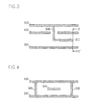
- multi-layered connection lines can be manufactured. In this case, the connection line each provided in a different layer can be connected via a second connection line 540 as shown in FIG. 3.
- connection states between the first connection line 510 and the passive element 310 will now be described.
- the passive element 310 is connected to the second connection line 540, which is connected to the first connection line 510 via an open area of the second electric shield line 400. Accordingly, the passive element 310 is electrically connected to the integrated circuits IC1, 1C2, ..., ICn via the connection lines 510 and 540. Also, when a plurality of passive elements is necessary, the passive elements can be manufactured in a multi-layered manner, and in this case, the passive elements each provided in a different layer can be connected via the second connection line 540.
- FIG. 4 shows a cross-sectional view of FIG. 3 cut with a line C-C'.
- the passive element 310 is surrounded by the first and second electric shield lines 200 and 400 and is electrically shielded, signal interference between the passive element 310 and the first connection line 510 can be reduced. If needed, additional electric shield lines 320 and 330 can be provided to electrically shield other passive elements 310.
- the passive elements 310 comprise the resistors, the inductors and the capacitors.
- Resistance values depend on material and physical structure of the passive elements 310, that is, width and length of the passive elements. In the preferred embodiment of the present invention, the resistance values are mainly obtained by optimizing the physical structure of the passive elements.
- the inductors can be obtained by arranging metallic passive elements in a zigzag manner on a plane as shown in FIG, 5(a), in a spiral manner as shown in FIG. 5(b), or in other manners.
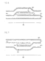
- FIG. 6 shows the capacitor according to the preferred embodiment of the present invention.
- the capacitor is obtained by providing first and second metal layers 312 and 314 between the first and second electric shield lines 200 and 400, and inserting a dielectric 316 into an area where the first and second metal layers 312 and 314 are superimposed.
- a length from the first metal layer 312 to the second metal layer 314 is set to be a, and a length from the second metal layer 314 to the second electric shield line 400 to be ⁇ , it is preferable to design the value of ⁇ / ⁇ to be fully greater than 1. Further, it is also preferable to make the length from the first electric shield line 200 to the first metal layer 312 almost identical with the length from the second electric shield line 400 to the second metal layer 314.
- the first electric shield line 200 and the first metal layer 312 are planar as shown in FIG. 6, but the second electric shield line 400 and the second metal layer 314 are bent, and thereby following processes can become difficult.
- the capacitor on the groove 210 of the semiconductor substrate as shown in FIG. 7. Then, the first electric shield line 200 and the first metal layer 312 are partially bent, and the second electric shield line 400 and the second metal layer 314 become flat, and therefore, following processes can be smoothly performed. At this time, it is preferable to use the chemical mechanical polishing (CMP) process so as to make the second electric shield line 400 and the second metal layer 314 flat. It is also possible to provide the inductor on the groove 210 of the semiconductor substrate in the same manner of manufacturing the capacitor.
- CMP chemical mechanical polishing
- an IC for processing the RF signals and an IC for processing the base band signals are mounted on the bumper 700, and the passive elements such as the resistors, capacitors and inductors are mounted on a passive element layer, and the passive elements and the ICs are connected via the connection line on the interconnection layer. Therefore, the sizes of the terminals can be reduced.
- the semiconductor substrate is used, but other types of substrates can also be used.
- the base band unit and the RF unit can be formed into a single module.
- the size of the module can be reduced since the ICs and the passive elements are provided in the different layers.
Landscapes
- Semiconductor Integrated Circuits (AREA)
- Shielding Devices Or Components To Electric Or Magnetic Fields (AREA)
- Production Of Multi-Layered Print Wiring Board (AREA)
Applications Claiming Priority (2)
| Application Number | Priority Date | Filing Date | Title |
|---|---|---|---|
| KR0008822 | 2000-02-23 | ||
| KR1020000008822A KR100308872B1 (ko) | 2000-02-23 | 2000-02-23 | 다층 멀티칩 모듈 |
Publications (2)
| Publication Number | Publication Date |
|---|---|
| EP1128434A2 true EP1128434A2 (de) | 2001-08-29 |
| EP1128434A3 EP1128434A3 (de) | 2008-05-07 |
Family
ID=19649253
Family Applications (1)
| Application Number | Title | Priority Date | Filing Date |
|---|---|---|---|
| EP00123414A Withdrawn EP1128434A3 (de) | 2000-02-23 | 2000-11-02 | Mehrschicht-Mehrchip-Modul für Hochfrequenzen |
Country Status (6)
| Country | Link |
|---|---|
| EP (1) | EP1128434A3 (de) |
| JP (1) | JP2001244402A (de) |
| KR (1) | KR100308872B1 (de) |
| AU (1) | AU1060201A (de) |
| TW (1) | TW466745B (de) |
| WO (1) | WO2001063646A2 (de) |
Cited By (10)
| Publication number | Priority date | Publication date | Assignee | Title |
|---|---|---|---|---|
| WO2003053113A1 (en) * | 2001-12-14 | 2003-06-26 | Optillion Ab | Feedthrough interconnection assembly |
| EP1342398A4 (de) * | 2000-12-15 | 2008-10-29 | X2Y Attenuators Llc | Energieweganordnungen zur energieaufbereitung |
| US7593208B2 (en) | 1997-04-08 | 2009-09-22 | X2Y Attenuators, Llc | Multi-functional energy conditioner |
| US7609500B2 (en) | 1997-04-08 | 2009-10-27 | X2Y Attenuators, Llc | Universal energy conditioning interposer with circuit architecture |
| US7688565B2 (en) | 1997-04-08 | 2010-03-30 | X2Y Attenuators, Llc | Arrangements for energy conditioning |
| US7768763B2 (en) | 1997-04-08 | 2010-08-03 | X2Y Attenuators, Llc | Arrangement for energy conditioning |
| US7782587B2 (en) | 2005-03-01 | 2010-08-24 | X2Y Attenuators, Llc | Internally overlapped conditioners |
| US8014119B2 (en) | 2005-03-01 | 2011-09-06 | X2Y Attenuators, Llc | Energy conditioner with tied through electrodes |
| US8026777B2 (en) * | 2006-03-07 | 2011-09-27 | X2Y Attenuators, Llc | Energy conditioner structures |
| US9054094B2 (en) | 1997-04-08 | 2015-06-09 | X2Y Attenuators, Llc | Energy conditioning circuit arrangement for integrated circuit |
Families Citing this family (5)
| Publication number | Priority date | Publication date | Assignee | Title |
|---|---|---|---|---|
| US8421158B2 (en) | 1998-12-21 | 2013-04-16 | Megica Corporation | Chip structure with a passive device and method for forming the same |
| JP4529262B2 (ja) * | 2000-09-14 | 2010-08-25 | ソニー株式会社 | 高周波モジュール装置及びその製造方法 |
| US6744129B2 (en) | 2002-01-11 | 2004-06-01 | Microtune (San Diego), Inc. | Integrated ground shield |
| EP2455011A3 (de) | 2002-08-21 | 2017-09-13 | Olympus Corporation | Bindungsvorrichtung für biologisches Gewebe |
| KR101382768B1 (ko) * | 2007-08-20 | 2014-04-17 | 엘지이노텍 주식회사 | 스태킹 구조의 칩 소자 |
Family Cites Families (8)
| Publication number | Priority date | Publication date | Assignee | Title |
|---|---|---|---|---|
| JP3661704B2 (ja) * | 1992-04-01 | 2005-06-22 | 株式会社村田製作所 | 多層セラミック基板 |
| JPH06125180A (ja) * | 1992-10-09 | 1994-05-06 | Ngk Spark Plug Co Ltd | キャパシタ内蔵多層配線基板 |
| US5410107A (en) * | 1993-03-01 | 1995-04-25 | The Board Of Trustees Of The University Of Arkansas | Multichip module |
| JPH07193184A (ja) * | 1993-12-27 | 1995-07-28 | Fujitsu Ltd | マルチチップモジュールの製造方法及びマルチチップモジュール |
| JPH07335779A (ja) * | 1994-06-08 | 1995-12-22 | Fujitsu Ltd | マルチチップモジュール |
| JPH088393A (ja) * | 1994-06-23 | 1996-01-12 | Fujitsu Ltd | 半導体装置 |
| US5777383A (en) * | 1996-05-09 | 1998-07-07 | Lsi Logic Corporation | Semiconductor chip package with interconnect layers and routing and testing methods |
| JPH1145977A (ja) * | 1997-07-28 | 1999-02-16 | Hitachi Ltd | マルチチップモジュールおよびその製造方法 |
-
2000
- 2000-02-23 KR KR1020000008822A patent/KR100308872B1/ko not_active Expired - Fee Related
- 2000-10-26 WO PCT/KR2000/001211 patent/WO2001063646A2/en not_active Ceased
- 2000-10-26 AU AU10602/01A patent/AU1060201A/en not_active Abandoned
- 2000-11-02 EP EP00123414A patent/EP1128434A3/de not_active Withdrawn
- 2000-11-02 TW TW089123047A patent/TW466745B/zh not_active IP Right Cessation
- 2000-11-06 JP JP2000338062A patent/JP2001244402A/ja active Pending
Cited By (24)
| Publication number | Priority date | Publication date | Assignee | Title |
|---|---|---|---|---|
| US8004812B2 (en) | 1997-04-08 | 2011-08-23 | X2Y Attenuators, Llc | Energy conditioning circuit arrangement for integrated circuit |
| US7916444B2 (en) | 1997-04-08 | 2011-03-29 | X2Y Attenuators, Llc | Arrangement for energy conditioning |
| US7593208B2 (en) | 1997-04-08 | 2009-09-22 | X2Y Attenuators, Llc | Multi-functional energy conditioner |
| US7609500B2 (en) | 1997-04-08 | 2009-10-27 | X2Y Attenuators, Llc | Universal energy conditioning interposer with circuit architecture |
| US7609501B2 (en) | 1997-04-08 | 2009-10-27 | X2Y Attenuators, Llc | Manufacture including shield structure |
| US7688565B2 (en) | 1997-04-08 | 2010-03-30 | X2Y Attenuators, Llc | Arrangements for energy conditioning |
| US9373592B2 (en) | 1997-04-08 | 2016-06-21 | X2Y Attenuators, Llc | Arrangement for energy conditioning |
| US7768763B2 (en) | 1997-04-08 | 2010-08-03 | X2Y Attenuators, Llc | Arrangement for energy conditioning |
| US9054094B2 (en) | 1997-04-08 | 2015-06-09 | X2Y Attenuators, Llc | Energy conditioning circuit arrangement for integrated circuit |
| US8587915B2 (en) | 1997-04-08 | 2013-11-19 | X2Y Attenuators, Llc | Arrangement for energy conditioning |
| US7920367B2 (en) | 1997-04-08 | 2011-04-05 | X2Y Attenuators, Llc | Method for making arrangement for energy conditioning |
| US7733621B2 (en) | 1997-04-08 | 2010-06-08 | X2Y Attenuators, Llc | Energy conditioning circuit arrangement for integrated circuit |
| US9036319B2 (en) | 1997-04-08 | 2015-05-19 | X2Y Attenuators, Llc | Arrangement for energy conditioning |
| US9019679B2 (en) | 1997-04-08 | 2015-04-28 | X2Y Attenuators, Llc | Arrangement for energy conditioning |
| US8018706B2 (en) | 1997-04-08 | 2011-09-13 | X2Y Attenuators, Llc | Arrangement for energy conditioning |
| US8023241B2 (en) | 1997-04-08 | 2011-09-20 | X2Y Attenuators, Llc | Arrangement for energy conditioning |
| EP1342398A4 (de) * | 2000-12-15 | 2008-10-29 | X2Y Attenuators Llc | Energieweganordnungen zur energieaufbereitung |
| WO2003053113A1 (en) * | 2001-12-14 | 2003-06-26 | Optillion Ab | Feedthrough interconnection assembly |
| US8547677B2 (en) | 2005-03-01 | 2013-10-01 | X2Y Attenuators, Llc | Method for making internally overlapped conditioners |
| US9001486B2 (en) | 2005-03-01 | 2015-04-07 | X2Y Attenuators, Llc | Internally overlapped conditioners |
| US8014119B2 (en) | 2005-03-01 | 2011-09-06 | X2Y Attenuators, Llc | Energy conditioner with tied through electrodes |
| US7782587B2 (en) | 2005-03-01 | 2010-08-24 | X2Y Attenuators, Llc | Internally overlapped conditioners |
| US7974062B2 (en) | 2005-03-01 | 2011-07-05 | X2Y Attenuators, Llc | Internally overlapped conditioners |
| US8026777B2 (en) * | 2006-03-07 | 2011-09-27 | X2Y Attenuators, Llc | Energy conditioner structures |
Also Published As
| Publication number | Publication date |
|---|---|
| AU1060201A (en) | 2001-09-03 |
| WO2001063646A3 (en) | 2002-05-30 |
| TW466745B (en) | 2001-12-01 |
| KR100308872B1 (ko) | 2001-11-03 |
| WO2001063646A2 (en) | 2001-08-30 |
| JP2001244402A (ja) | 2001-09-07 |
| KR20000071919A (ko) | 2000-12-05 |
| EP1128434A3 (de) | 2008-05-07 |
Similar Documents
| Publication | Publication Date | Title |
|---|---|---|
| JP3941911B2 (ja) | 集積rf性能を備えたマルチチップモジュール | |
| EP1573813B1 (de) | Rf leistungstransistor mit innerer vorspannungsversorgung | |
| US6418032B2 (en) | Printed wiring board | |
| CN1224094C (zh) | 集成射频电路 | |
| US7859383B2 (en) | Spiral inductor with multi-trace structure | |
| JP3874241B2 (ja) | 電子部品および設計方法 | |
| US6191479B1 (en) | Decoupling capacitor configuration for integrated circuit chip | |
| WO2001063646A2 (en) | Multi-layered multi-chip module | |
| US20080012097A1 (en) | Semiconductor device and wireless device using the semiconductor device | |
| US7795709B2 (en) | Shielding noisy conductors in integrated passive devices | |
| JPH10256826A (ja) | 同調型スロットアンテナ | |
| US6933597B1 (en) | Spacer with passive components for use in multi-chip modules | |
| EP1104026B1 (de) | Massebene für ein IC | |
| WO2000051012A2 (en) | Integrated circuit interconnect system | |
| JPH07263506A (ja) | 集積回路のテスト装置 | |
| US6982879B1 (en) | Apparatus to provide connection between a microelectronic device and an antenna | |
| WO2006018769A1 (en) | Wireless terminal, wireless module and method of manufacturing such a terminal. | |
| US20060138650A1 (en) | Integrated circuit packaging device and method for matching impedance | |
| WO2000075990A1 (en) | High impedance matched rf power transistor | |
| US10756027B1 (en) | Semiconductor structure and method for forming the same | |
| CN1868065A (zh) | 具有由多环结构形成的电感环的集成电路封装 | |
| US20090085158A1 (en) | Package with improved connection of a decoupling capacitor | |
| EP1111969B1 (de) | Verfahren und Struktur zur Reduzierung des Leistungsrauschens | |
| US20250029953A1 (en) | Inter-Terminal Die-to-Die Attachment | |
| JP2001167974A (ja) | 回路基板およびそれを用いた回路モジュールおよびそれを用いた電子装置 |
Legal Events
| Date | Code | Title | Description |
|---|---|---|---|
| PUAI | Public reference made under article 153(3) epc to a published international application that has entered the european phase |
Free format text: ORIGINAL CODE: 0009012 |
|
| AK | Designated contracting states |
Kind code of ref document: A2 Designated state(s): AT BE CH CY DE DK ES FI FR GB GR IE IT LI LU MC NL PT SE TR |
|
| AX | Request for extension of the european patent |
Free format text: AL;LT;LV;MK;RO;SI |
|
| PUAL | Search report despatched |
Free format text: ORIGINAL CODE: 0009013 |
|
| AK | Designated contracting states |
Kind code of ref document: A3 Designated state(s): AT BE CH CY DE DK ES FI FR GB GR IE IT LI LU MC NL PT SE TR |
|
| AX | Request for extension of the european patent |
Extension state: AL LT LV MK RO SI |
|
| STAA | Information on the status of an ep patent application or granted ep patent |
Free format text: STATUS: THE APPLICATION IS DEEMED TO BE WITHDRAWN |
|
| 18D | Application deemed to be withdrawn |
Effective date: 20080531 |