EP1104026B1 - Massebene für ein IC - Google Patents
Massebene für ein IC Download PDFInfo
- Publication number
- EP1104026B1 EP1104026B1 EP00309739A EP00309739A EP1104026B1 EP 1104026 B1 EP1104026 B1 EP 1104026B1 EP 00309739 A EP00309739 A EP 00309739A EP 00309739 A EP00309739 A EP 00309739A EP 1104026 B1 EP1104026 B1 EP 1104026B1
- Authority
- EP
- European Patent Office
- Prior art keywords
- semiconductor chip
- capacitor plate
- supporting member
- chip package
- package according
- Prior art date
- Legal status (The legal status is an assumption and is not a legal conclusion. Google has not performed a legal analysis and makes no representation as to the accuracy of the status listed.)
- Expired - Lifetime
Links
Images

Classifications
-
- H—ELECTRICITY
- H10—SEMICONDUCTOR DEVICES; ELECTRIC SOLID-STATE DEVICES NOT OTHERWISE PROVIDED FOR
- H10W—GENERIC PACKAGES, INTERCONNECTIONS, CONNECTORS OR OTHER CONSTRUCTIONAL DETAILS OF DEVICES COVERED BY CLASS H10
- H10W44/00—Electrical arrangements for controlling or matching impedance
- H10W44/601—Capacitive arrangements
-
- H—ELECTRICITY
- H10—SEMICONDUCTOR DEVICES; ELECTRIC SOLID-STATE DEVICES NOT OTHERWISE PROVIDED FOR
- H10W—GENERIC PACKAGES, INTERCONNECTIONS, CONNECTORS OR OTHER CONSTRUCTIONAL DETAILS OF DEVICES COVERED BY CLASS H10
- H10W42/00—Arrangements for protection of devices
-
- H—ELECTRICITY
- H10—SEMICONDUCTOR DEVICES; ELECTRIC SOLID-STATE DEVICES NOT OTHERWISE PROVIDED FOR
- H10W—GENERIC PACKAGES, INTERCONNECTIONS, CONNECTORS OR OTHER CONSTRUCTIONAL DETAILS OF DEVICES COVERED BY CLASS H10
- H10W72/00—Interconnections or connectors in packages
-
- H—ELECTRICITY
- H10—SEMICONDUCTOR DEVICES; ELECTRIC SOLID-STATE DEVICES NOT OTHERWISE PROVIDED FOR
- H10W—GENERIC PACKAGES, INTERCONNECTIONS, CONNECTORS OR OTHER CONSTRUCTIONAL DETAILS OF DEVICES COVERED BY CLASS H10
- H10W72/00—Interconnections or connectors in packages
- H10W72/071—Connecting or disconnecting
- H10W72/075—Connecting or disconnecting of bond wires
-
- H—ELECTRICITY
- H10—SEMICONDUCTOR DEVICES; ELECTRIC SOLID-STATE DEVICES NOT OTHERWISE PROVIDED FOR
- H10W—GENERIC PACKAGES, INTERCONNECTIONS, CONNECTORS OR OTHER CONSTRUCTIONAL DETAILS OF DEVICES COVERED BY CLASS H10
- H10W72/00—Interconnections or connectors in packages
- H10W72/50—Bond wires
- H10W72/531—Shapes of wire connectors
- H10W72/536—Shapes of wire connectors the connected ends being ball-shaped
-
- H—ELECTRICITY
- H10—SEMICONDUCTOR DEVICES; ELECTRIC SOLID-STATE DEVICES NOT OTHERWISE PROVIDED FOR
- H10W—GENERIC PACKAGES, INTERCONNECTIONS, CONNECTORS OR OTHER CONSTRUCTIONAL DETAILS OF DEVICES COVERED BY CLASS H10
- H10W72/00—Interconnections or connectors in packages
- H10W72/50—Bond wires
- H10W72/531—Shapes of wire connectors
- H10W72/5363—Shapes of wire connectors the connected ends being wedge-shaped
-
- H—ELECTRICITY
- H10—SEMICONDUCTOR DEVICES; ELECTRIC SOLID-STATE DEVICES NOT OTHERWISE PROVIDED FOR
- H10W—GENERIC PACKAGES, INTERCONNECTIONS, CONNECTORS OR OTHER CONSTRUCTIONAL DETAILS OF DEVICES COVERED BY CLASS H10
- H10W72/00—Interconnections or connectors in packages
- H10W72/851—Dispositions of multiple connectors or interconnections
- H10W72/874—On different surfaces
- H10W72/884—Die-attach connectors and bond wires
-
- H—ELECTRICITY
- H10—SEMICONDUCTOR DEVICES; ELECTRIC SOLID-STATE DEVICES NOT OTHERWISE PROVIDED FOR
- H10W—GENERIC PACKAGES, INTERCONNECTIONS, CONNECTORS OR OTHER CONSTRUCTIONAL DETAILS OF DEVICES COVERED BY CLASS H10
- H10W72/00—Interconnections or connectors in packages
- H10W72/90—Bond pads, in general
- H10W72/951—Materials of bond pads
-
- H—ELECTRICITY
- H10—SEMICONDUCTOR DEVICES; ELECTRIC SOLID-STATE DEVICES NOT OTHERWISE PROVIDED FOR
- H10W—GENERIC PACKAGES, INTERCONNECTIONS, CONNECTORS OR OTHER CONSTRUCTIONAL DETAILS OF DEVICES COVERED BY CLASS H10
- H10W90/00—Package configurations
- H10W90/701—Package configurations characterised by the relative positions of pads or connectors relative to package parts
- H10W90/731—Package configurations characterised by the relative positions of pads or connectors relative to package parts of die-attach connectors
- H10W90/734—Package configurations characterised by the relative positions of pads or connectors relative to package parts of die-attach connectors between a chip and a stacked insulating package substrate, interposer or RDL
-
- H—ELECTRICITY
- H10—SEMICONDUCTOR DEVICES; ELECTRIC SOLID-STATE DEVICES NOT OTHERWISE PROVIDED FOR
- H10W—GENERIC PACKAGES, INTERCONNECTIONS, CONNECTORS OR OTHER CONSTRUCTIONAL DETAILS OF DEVICES COVERED BY CLASS H10
- H10W90/00—Package configurations
- H10W90/701—Package configurations characterised by the relative positions of pads or connectors relative to package parts
- H10W90/751—Package configurations characterised by the relative positions of pads or connectors relative to package parts of bond wires
- H10W90/754—Package configurations characterised by the relative positions of pads or connectors relative to package parts of bond wires between a chip and a stacked insulating package substrate, interposer or RDL
Definitions
- the present invention relates to the design and production of integrated circuits and to the packaging of such circuits, more specifically the proposed invention relates to a ground plane for a semiconductor chip adapted to be mounted on a supporting member in a chip package.
- the ground point of the die is connected to the exterior via a bonding wire connected between the die and the interposer (or leadframe).
- the impedance of the bonding wire is important at RF-frequencies, and this makes it difficult to realise a proper ground node on the die. If the die is made bigger in order to make the bonding wire shorter, this only moves the problem from the bonding wire to the die because the conductor on the die has to be longer.
- Another solution is to have multiple conductors in parallel. This is often used in RF-PA-stages, but is not really practical for large scale integrated circuits as the multiple connections take up a lot of space.
- US 4 617 586 describes a high-frequency circuit having a semiconductor circuit element arranged on a substrate, in which one of the output terminals of the semiconductor circuit element is electrically coupled to a ground plane through a capacitive element and metallized holes.
- US 5 077 633 describes attaching and grounding a chip on a substrate using a silver filled epoxy and a some conductive holes through the carrier substrate.
- the problem is solved by placing a metal-covered area on the interposer under the die. Vias on the interposer connect the area to the underside of the interposer.
- the die is glued to the area with conducting glue.
- a capacitor is thus formed, the capacitor being formed by the die substrate, the oxide layer on the underside of the die, and the conductive plate on the interposer.
- the RF-ground plane can be tuned to that frequency by choosing the dimensions of the associated conductors, and the thus the inductance of said conductors, so that the resonant frequency of said inductance and capacitor coincides with said working frequency.
- the impedance at said working frequency can be made extremely low, close to 2 Ohm.
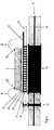
- Fig. 1 schematically shows a cross section of the preferred embodiment of a semiconductor chip and interposer assembly of an integrated circuit package according to the invention in a situation where the assembly is mounted on a printed circuit board (PCB).
- PCB printed circuit board
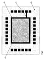
- Fig. 2 shows a top plan view of the chip and interposer assembly of fig. 1.
- Fig. 3 schematically shows an electric circuit diagram for the LC series circuit of the chip and interposer assembly of fig. 1.
- Fig. 4 schematically shows impedance characteristics for the bonding wire and via, and the total impedance, respectively, for the preferred embodiment.
- the semiconductor chip includes an insulating layer 2.
- this layer 2 would be an integrally formed layer comprising an oxide of the semiconductor material, i.e. silicon dioxide if the chip is made from silicon.
- the dielectric coefficient of silicon dioxide is app. 3.9.
- the chip 1 is glued to an insulating interposer 4 carrying a conductive area 5.
- the conductive area 5 is a metal covered area.
- the glue 3 is conductive and serves not only the purpose of adhering the chip 1 to the interposer 4, but also forms a capacitor plate, capacitively coupled to internal parts (not shown) of the chip, but insulated therefrom by the insulating layer 2.
- capacitor plates In the following these internal parts are referred to as capacitor plates regardless of their actual shape, i.e. all current carrying parts within the chip are considered as forming capacitor plates.
- PCB printed circuit board
- the capacitance value has been found to be approximately ten times higher when using conductive glue as compared to non-conductive glue.
- the vias 7 form a conducting member which connects the second capacitor plate to an exterior ground node according to the invention.
- each via 7 at the frequencies of interest only exhibits a relatively small impedance, it will in the envisaged applications be important to have a large number of vias 7 coupled in parallel in order to lower the impedance further over a range of frequencies.
- any conducting member exhibit an inductance.
- an LC series circuit is formed by the capacitance provided between internal parts of the chip and the conductive glue 3 separated by the dielectric layer 2, and the inductance provided by the vias 7. If the chip has a well defined working frequency, the number of vias may be chosen, so that the series resonant frequency of the inductance provided by the vias and the aforementioned capacitance, approximately matches the working frequency of the chip. In this way an extremely low ground impedance, 2 Ohms or less, can be achieved.
- the vias 7 in the preferred embodiment are not connected in parallel directly on the supporting interposer 4. Instead they are, as shown in fig. 1, connected in parallel via the conductive paths 16 on the printed circuit board 10 on which the chip package, containing the chip 1 and interposer 4 assembly according to the invention, is eventually mounted.
- the resonant frequency of the ground plane is influenced by the number of vias 7 actually connected in parallel for a given application, and by the way this is done, as well as by the inductance of the die and the layout of the PCB 10.
- a number of DC ground paths may be provided.
- a ground pad 13 is connected to a via 6 through a bonding wire 8 which in turn is connected to the PCB ground plane 12 by via 14.
- the impedance of this path is essentially inductive at the frequencies of interest.
- Another ground pad 15 is connected to conducting member 11 on interposer 4 through bonding wire 9 which is connected to the PCB ground plane 12 by vias 7. Either, or both, of the above described DC ground paths may be used. It should be noted that most circuits require at least one DC ground path.
- the DC ground paths may also be used for AC signals if very low ground impedance is not required.
- L 1 is the inductance of the die itself
- L 8 is the inductance of the bonding wire 8
- L 14 the inductance of the via 14
- C 5 the capacitance between internal parts of the chip 1 and the capacitor plate provided by the glue 3
- L 9 the inductance of bondwire 9
- L 11 the inductance of conducting member 11 on interposer 4
- L 7 the combined inductance of the vias 7, when they are eventually connected in parallel.
- Fig. 4 illustrates the difference between the impedance to ground when an AC-ground plane according to the invention is used (normal line), and when only the inductive DC ground is used (dotted line). Both axes are logarithmic.
- the dip in impedance at f 0 should be noted, since at this specific frequency the impedance of the ground path becomes virtually zero. Thus if this frequency f 0 matches the operating frequency of the chip, a very low impedance ground path is provided for the chip.
- f 0 is not tuned to the working frequency of the circuit the ground impedance obtained by using the AC-ground plane is still much lower that it would have been without it provided that the working frequency of the circuit is greater than f a
Landscapes
- Semiconductor Integrated Circuits (AREA)
- Structures For Mounting Electric Components On Printed Circuit Boards (AREA)
- Lead Frames For Integrated Circuits (AREA)
Claims (12)
- Halbleiterchipgehäuse, welches einen Halbleiterchip (1), eine Grundplatte, eine erste und zweite Kondensatorplatte und ein Trägerelement (4) umfasst, wobei die Grundplatte mindestens eine elektrisch leitende Durchkontaktierung (7) aufweist, die sich durch das Trägerelement (4) erstreckt, und elektrisch mit der zweiten Kondensatorplatte (3) gekoppelt ist, dadurch gekennzeichnet, dass die Grundplatte die in dem Chip bereitgestellte erste Kondensatorplatte und die auf dem Trägerelement (4) bereitgestellte zweite Kondensatorplatte (3, 5) umfasst, wobei die erste und zweite Kondensatorplatte durch eine dielektrische Schicht (2) voneinander getrennt sind, die die Platten kapazitiv aneinander koppelt.
- Halbleiterchipgehäuse nach Anspruch 1, wobei die Resonanzfrequenz der durch die erste Kondensatorplatte und die zweite Kondensatorplatte (3, 5) bereitgestellten Kapazität und der durch die Durchkontaktierung (7) bereitgestellten Induktivität ungefähr gleich der beabsichtigten Arbeitsfrequenz des Chips ist.
- Halbleiterchipgehäuse nach Anspruch 1 oder 2, dadurch gekennzeichnet, dass die dielektrische Schicht ein integraler Teil des Chips (1) ist.
- Halbleiterchipgehäuse nach Anspruch 3, dadurch gekennzeichnet, dass die dielektrische Schicht die gesamte Oberfläche des Chips bedeckt, welche in Richtung des Trägerelements (4) weist.
- Halbleiterchipgehäuse nach Anspruch 3 oder 4, dadurch gekennzeichnet, dass die dielektrische Schicht Siliziumdioxid umfasst.
- Halbleiterchipgehäuse nach einem der vorhergehenden Ansprüche, dadurch gekennzeichnet, dass die zweite Kondensatorplatte eine Schicht aus leitendem Kleber (3) umfasst.
- Halbleiterchipgehäuse nach irgendeinem der vorhergehenden Ansprüche, dadurch gekennzeichnet, dass die zweite Kondensatorplatte eine metallische Schicht (5) auf dem Trägerelement (4) umfasst.
- Halbleiterchipgehäuse nach Anspruch 6 oder 7, dadurch gekennzeichnet, dass die Schicht aus leitendem Kleber (3) zwischen der metallischen Schicht (5) und der dielektrischen Schicht (2) bereitgestellt ist.
- Halbleiterchipgehäuse nach irgendeinem der vorhergehenden Ansprüche, dadurch gekennzeichnet, dass mindestens eine elektrisch leitende Durchkontaktierung (7), die sich durch das Trägerelement erstreckt, direkt mit der zweiten Kondensatorplatte (3, 5) verbunden ist.
- Halbleiterchipgehäuse nach irgendeinem der Ansprüche 7, 8 oder 9, dadurch gekennzeichnet, dass die mindestens eine Durchkontaktierung und die metallische Schicht einstückig aus demselben Metall gebildet sind.
- Verfahren zum Bereitstellen einer Grundplatte für einen Halbleiterchip (1), der auf einem Trägerelement in einem Chipgehäuse angebracht ist, umfassend;Bereitstellen einer ersten Kondensatorplatte in dem Chip;Bereitstellen einer zweiten Kondensatorplatte (3,5) auf dem Trägerelement (4); undBereitstellen einer dielektrischen Schicht (2) zwischen der ersten und der zweiten Kondensatorplatte, welche die Platten kapazitiv miteinander koppelt, wobei das Verfahren weiter umfasst:Bereitstellen mindestens einer elektrisch leitenden Durchkontaktierung (7), die sich durch das Trägerelement (4) erstreckt und elektrisch an die zweite Kondensatorplatte (3) gekoppelt ist.
- Verfahren nach Anspruch 11, umfassend das Ankleben des Halbleiterchips an das Trägerelement mittels eines leitenden Klebers (3).
Applications Claiming Priority (2)
| Application Number | Priority Date | Filing Date | Title |
|---|---|---|---|
| GB9928080A GB2356737A (en) | 1999-11-26 | 1999-11-26 | Ground Plane for a Semiconductor Chip |
| GB9928080 | 1999-11-26 |
Publications (3)
| Publication Number | Publication Date |
|---|---|
| EP1104026A2 EP1104026A2 (de) | 2001-05-30 |
| EP1104026A3 EP1104026A3 (de) | 2003-08-13 |
| EP1104026B1 true EP1104026B1 (de) | 2006-02-01 |
Family
ID=10865277
Family Applications (1)
| Application Number | Title | Priority Date | Filing Date |
|---|---|---|---|
| EP00309739A Expired - Lifetime EP1104026B1 (de) | 1999-11-26 | 2000-11-03 | Massebene für ein IC |
Country Status (5)
| Country | Link |
|---|---|
| US (1) | US6608259B1 (de) |
| EP (1) | EP1104026B1 (de) |
| JP (1) | JP2001168234A (de) |
| DE (1) | DE60025796T2 (de) |
| GB (1) | GB2356737A (de) |
Families Citing this family (20)
| Publication number | Priority date | Publication date | Assignee | Title |
|---|---|---|---|---|
| US6643916B2 (en) * | 2001-05-18 | 2003-11-11 | Hewlett-Packard Development Company, L.P. | Method to assemble a capacitor plate for substrate components |
| US20020170897A1 (en) * | 2001-05-21 | 2002-11-21 | Hall Frank L. | Methods for preparing ball grid array substrates via use of a laser |
| US6812064B2 (en) * | 2001-11-07 | 2004-11-02 | Micron Technology, Inc. | Ozone treatment of a ground semiconductor die to improve adhesive bonding to a substrate |
| US6948943B2 (en) * | 2002-03-06 | 2005-09-27 | Intel Corporation | Shunting arrangements to reduce high currents in grid array connectors |
| EP1471575A1 (de) * | 2003-04-24 | 2004-10-27 | Samsung Electronics Co., Ltd. | RF Chipträger mit integrierten Induktoren und Verfahren zu seiner Herstellung |
| US7414505B2 (en) | 2003-05-13 | 2008-08-19 | Samsung Electronics Co., Ltd. | High frequency inductor having low inductance and low inductance variation and method of manufacturing the same |
| US7245023B1 (en) | 2004-06-11 | 2007-07-17 | Bridge Semiconductor Corporation | Semiconductor chip assembly with solder-attached ground plane |
| US7157791B1 (en) | 2004-06-11 | 2007-01-02 | Bridge Semiconductor Corporation | Semiconductor chip assembly with press-fit ground plane |
| US7294791B2 (en) * | 2004-09-29 | 2007-11-13 | Endicott Interconnect Technologies, Inc. | Circuitized substrate with improved impedance control circuitry, method of making same, electrical assembly and information handling system utilizing same |
| JP2007080969A (ja) * | 2005-09-12 | 2007-03-29 | Sony Corp | プリント配線板及びプリント配線板の製造方法 |
| US7510928B2 (en) * | 2006-05-05 | 2009-03-31 | Tru-Si Technologies, Inc. | Dielectric trenches, nickel/tantalum oxide structures, and chemical mechanical polishing techniques |
| WO2007146665A2 (en) * | 2006-06-06 | 2007-12-21 | Teraspeed Consulting Group, Llc | Power distribution system for integrated circuits |
| US7479015B2 (en) * | 2006-06-30 | 2009-01-20 | Intel Corporation | Socket assembly that includes improved contact arrangement |
| JP4760789B2 (ja) * | 2006-08-21 | 2011-08-31 | 株式会社村田製作所 | 積層コンデンサ、回路基板及び回路モジュール |
| JP2010034403A (ja) * | 2008-07-30 | 2010-02-12 | Shinko Electric Ind Co Ltd | 配線基板及び電子部品装置 |
| FR2969398B1 (fr) * | 2010-12-20 | 2013-01-11 | St Microelectronics Sa | Emetteur-recepteur integre en ondes millimetriques |
| FR2969397B1 (fr) | 2010-12-20 | 2013-09-06 | St Microelectronics Crolles 2 | Emetteur-recepteur integre en ondes millimetriques |
| US9241400B2 (en) | 2013-08-23 | 2016-01-19 | Seagate Technology Llc | Windowed reference planes for embedded conductors |
| US10418298B2 (en) * | 2013-09-24 | 2019-09-17 | STATS ChipPAC Pte. Ltd. | Semiconductor device and method of forming dual fan-out semiconductor package |
| US9400529B2 (en) * | 2013-09-27 | 2016-07-26 | Apple Inc. | Electronic device having housing with embedded interconnects |
Family Cites Families (20)
| Publication number | Priority date | Publication date | Assignee | Title |
|---|---|---|---|---|
| DE2902002A1 (de) * | 1979-01-19 | 1980-07-31 | Gerhard Krause | Dreidimensional integrierte elektronische schaltungen |
| FR2524712B1 (fr) * | 1982-03-31 | 1985-06-07 | Radiotechnique Compelec | Circuit hyperfrequence a condensateur integre et application a un circuit d'alimentation |
| US4665468A (en) * | 1984-07-10 | 1987-05-12 | Nec Corporation | Module having a ceramic multi-layer substrate and a multi-layer circuit thereupon, and process for manufacturing the same |
| US5210599A (en) * | 1988-09-30 | 1993-05-11 | Fujitsu Limited | Semiconductor device having a built-in capacitor and manufacturing method thereof |
| US4954197A (en) * | 1989-03-30 | 1990-09-04 | Xerox Corporation | Process for assembling smaller arrays together to form a longer array |
| US5077633A (en) * | 1989-05-01 | 1991-12-31 | Motorola Inc. | Grounding an ultra high density pad array chip carrier |
| JPH04291949A (ja) * | 1991-03-20 | 1992-10-16 | Fujitsu Ltd | 半導体装置の実装装置 |
| US5309324A (en) * | 1991-11-26 | 1994-05-03 | Herandez Jorge M | Device for interconnecting integrated circuit packages to circuit boards |
| US5307237A (en) * | 1992-08-31 | 1994-04-26 | Hewlett-Packard Company | Integrated circuit packaging with improved heat transfer and reduced signal degradation |
| DE9308842U1 (de) * | 1993-06-14 | 1993-07-22 | Blaupunkt-Werke Gmbh, 31139 Hildesheim | Elektrische Baugruppe |
| US5475317A (en) * | 1993-12-23 | 1995-12-12 | Epi Technologies, Inc. | Singulated bare die tester and method of performing forced temperature electrical tests and burn-in |
| US5741729A (en) * | 1994-07-11 | 1998-04-21 | Sun Microsystems, Inc. | Ball grid array package for an integrated circuit |
| DE4429289A1 (de) * | 1994-08-18 | 1996-02-22 | Telefunken Microelectron | Integrierte Schaltungsanordnung |
| JP3472430B2 (ja) * | 1997-03-21 | 2003-12-02 | シャープ株式会社 | アンテナ一体化高周波回路 |
| US5798567A (en) * | 1997-08-21 | 1998-08-25 | Hewlett-Packard Company | Ball grid array integrated circuit package which employs a flip chip integrated circuit and decoupling capacitors |
| DE69839597D1 (de) * | 1998-01-13 | 2008-07-24 | Lucent Technologies Inc | Hochfrequenzhalbleiteranordnung |
| US5939782A (en) * | 1998-03-03 | 1999-08-17 | Sun Microsystems, Inc. | Package construction for integrated circuit chip with bypass capacitor |
| US6400576B1 (en) * | 1999-04-05 | 2002-06-04 | Sun Microsystems, Inc. | Sub-package bypass capacitor mounting for an array packaged integrated circuit |
| US6407929B1 (en) * | 2000-06-29 | 2002-06-18 | Intel Corporation | Electronic package having embedded capacitors and method of fabrication therefor |
| US6388207B1 (en) * | 2000-12-29 | 2002-05-14 | Intel Corporation | Electronic assembly with trench structures and methods of manufacture |
-
1999
- 1999-11-26 GB GB9928080A patent/GB2356737A/en not_active Withdrawn
-
2000
- 2000-11-03 DE DE60025796T patent/DE60025796T2/de not_active Expired - Lifetime
- 2000-11-03 EP EP00309739A patent/EP1104026B1/de not_active Expired - Lifetime
- 2000-11-24 JP JP2000357110A patent/JP2001168234A/ja active Pending
- 2000-11-27 US US09/721,677 patent/US6608259B1/en not_active Expired - Fee Related
Also Published As
| Publication number | Publication date |
|---|---|
| DE60025796T2 (de) | 2006-10-12 |
| GB2356737A (en) | 2001-05-30 |
| EP1104026A2 (de) | 2001-05-30 |
| US6608259B1 (en) | 2003-08-19 |
| DE60025796D1 (de) | 2006-04-13 |
| EP1104026A3 (de) | 2003-08-13 |
| JP2001168234A (ja) | 2001-06-22 |
| GB9928080D0 (en) | 2000-01-26 |
Similar Documents
| Publication | Publication Date | Title |
|---|---|---|
| US6608259B1 (en) | Ground plane for a semiconductor chip | |
| CN103681635B (zh) | 具有阻抗匹配电路的半导体装置及其制造方法 | |
| US5982018A (en) | Thin film capacitor coupons for memory modules and multi-chip modules | |
| US6377464B1 (en) | Multiple chip module with integrated RF capabilities | |
| US7033934B2 (en) | Method of production of semiconductor package | |
| US6191479B1 (en) | Decoupling capacitor configuration for integrated circuit chip | |
| US6486535B2 (en) | Electronic package with surface-mountable device built therein | |
| JPS6352781B2 (de) | ||
| TWI566350B (zh) | Semiconductor device | |
| US6636416B2 (en) | Electronic assembly with laterally connected capacitors and manufacturing method | |
| CN1937306A (zh) | 微波电路封装的端口和安装在该封装中的微波部件的互连 | |
| JP3743427B2 (ja) | 電磁波シールド型半導体装置 | |
| US6529105B1 (en) | Process and device for bonding two millimeter elements | |
| JP2001352000A (ja) | インターポーザを使用した高周波用半導体装置 | |
| JPS6256664B2 (de) | ||
| US8039957B2 (en) | System for improving flip chip performance | |
| JPH0936617A (ja) | 高周波モジュール | |
| US20240292520A1 (en) | Matching circuit board and semiconductor device | |
| JP5459335B2 (ja) | パッケージ基板及び半導体パッケージ | |
| US20050280134A1 (en) | Multi-frequency noise suppression capacitor set | |
| KR20100035100A (ko) | 커패시턴스를 사용한 칩 패키지의 도금 스터브 반사 최소화 기법 | |
| JPS6035247Y2 (ja) | 半導体装置 | |
| JPS634662A (ja) | 電子回路装置 | |
| JPH05211279A (ja) | 混成集積回路 | |
| JPH0432252A (ja) | 電子部品搭載用基板 |
Legal Events
| Date | Code | Title | Description |
|---|---|---|---|
| PUAI | Public reference made under article 153(3) epc to a published international application that has entered the european phase |
Free format text: ORIGINAL CODE: 0009012 |
|
| AK | Designated contracting states |
Kind code of ref document: A2 Designated state(s): AT BE CH CY DE DK ES FI FR GB GR IE IT LI LU MC NL PT SE TR |
|
| AX | Request for extension of the european patent |
Free format text: AL;LT;LV;MK;RO;SI |
|
| RAP1 | Party data changed (applicant data changed or rights of an application transferred) |
Owner name: NOKIA CORPORATION |
|
| PUAL | Search report despatched |
Free format text: ORIGINAL CODE: 0009013 |
|
| AK | Designated contracting states |
Designated state(s): AT BE CH CY DE DK ES FI FR GB GR IE IT LI LU MC NL PT SE TR |
|
| AX | Request for extension of the european patent |
Extension state: AL LT LV MK RO SI |
|
| 17P | Request for examination filed |
Effective date: 20040213 |
|
| AKX | Designation fees paid |
Designated state(s): DE FR IT SE |
|
| 17Q | First examination report despatched |
Effective date: 20040428 |
|
| GRAP | Despatch of communication of intention to grant a patent |
Free format text: ORIGINAL CODE: EPIDOSNIGR1 |
|
| GRAS | Grant fee paid |
Free format text: ORIGINAL CODE: EPIDOSNIGR3 |
|
| GRAA | (expected) grant |
Free format text: ORIGINAL CODE: 0009210 |
|
| AK | Designated contracting states |
Kind code of ref document: B1 Designated state(s): DE FR IT SE |
|
| PG25 | Lapsed in a contracting state [announced via postgrant information from national office to epo] |
Ref country code: IT Free format text: LAPSE BECAUSE OF FAILURE TO SUBMIT A TRANSLATION OF THE DESCRIPTION OR TO PAY THE FEE WITHIN THE PRESCRIBED TIME-LIMIT;WARNING: LAPSES OF ITALIAN PATENTS WITH EFFECTIVE DATE BEFORE 2007 MAY HAVE OCCURRED AT ANY TIME BEFORE 2007. THE CORRECT EFFECTIVE DATE MAY BE DIFFERENT FROM THE ONE RECORDED. Effective date: 20060201 |
|
| REF | Corresponds to: |
Ref document number: 60025796 Country of ref document: DE Date of ref document: 20060413 Kind code of ref document: P |
|
| PG25 | Lapsed in a contracting state [announced via postgrant information from national office to epo] |
Ref country code: SE Free format text: LAPSE BECAUSE OF FAILURE TO SUBMIT A TRANSLATION OF THE DESCRIPTION OR TO PAY THE FEE WITHIN THE PRESCRIBED TIME-LIMIT Effective date: 20060501 |
|
| ET | Fr: translation filed | ||
| PLBE | No opposition filed within time limit |
Free format text: ORIGINAL CODE: 0009261 |
|
| STAA | Information on the status of an ep patent application or granted ep patent |
Free format text: STATUS: NO OPPOSITION FILED WITHIN TIME LIMIT |
|
| 26N | No opposition filed |
Effective date: 20061103 |
|
| PGFP | Annual fee paid to national office [announced via postgrant information from national office to epo] |
Ref country code: DE Payment date: 20091029 Year of fee payment: 10 |
|
| PGFP | Annual fee paid to national office [announced via postgrant information from national office to epo] |
Ref country code: IT Payment date: 20091112 Year of fee payment: 10 Ref country code: FR Payment date: 20091123 Year of fee payment: 10 |
|
| REG | Reference to a national code |
Ref country code: FR Ref legal event code: ST Effective date: 20110801 |
|
| REG | Reference to a national code |
Ref country code: DE Ref legal event code: R119 Ref document number: 60025796 Country of ref document: DE Effective date: 20110601 Ref country code: DE Ref legal event code: R119 Ref document number: 60025796 Country of ref document: DE Effective date: 20110531 |
|
| PG25 | Lapsed in a contracting state [announced via postgrant information from national office to epo] |
Ref country code: DE Free format text: LAPSE BECAUSE OF NON-PAYMENT OF DUE FEES Effective date: 20110531 |
|
| PG25 | Lapsed in a contracting state [announced via postgrant information from national office to epo] |
Ref country code: FR Free format text: LAPSE BECAUSE OF NON-PAYMENT OF DUE FEES Effective date: 20101130 |
|
| PG25 | Lapsed in a contracting state [announced via postgrant information from national office to epo] |
Ref country code: IT Free format text: LAPSE BECAUSE OF NON-PAYMENT OF DUE FEES Effective date: 20101103 |