EP1123525B2 - Dispositif et procede pour l'examen optique de brasures cachees - Google Patents
Dispositif et procede pour l'examen optique de brasures cachees Download PDFInfo
- Publication number
- EP1123525B2 EP1123525B2 EP99953551A EP99953551A EP1123525B2 EP 1123525 B2 EP1123525 B2 EP 1123525B2 EP 99953551 A EP99953551 A EP 99953551A EP 99953551 A EP99953551 A EP 99953551A EP 1123525 B2 EP1123525 B2 EP 1123525B2
- Authority
- EP
- European Patent Office
- Prior art keywords
- head
- lens head
- image
- illuminating device
- lens
- Prior art date
- Legal status (The legal status is an assumption and is not a legal conclusion. Google has not performed a legal analysis and makes no representation as to the accuracy of the status listed.)
- Expired - Lifetime
Links
Images

Classifications
-
- G—PHYSICS
- G01—MEASURING; TESTING
- G01B—MEASURING LENGTH, THICKNESS OR SIMILAR LINEAR DIMENSIONS; MEASURING ANGLES; MEASURING AREAS; MEASURING IRREGULARITIES OF SURFACES OR CONTOURS
- G01B11/00—Measuring arrangements characterised by the use of optical techniques
- G01B11/30—Measuring arrangements characterised by the use of optical techniques for measuring roughness or irregularity of surfaces
-
- G—PHYSICS
- G01—MEASURING; TESTING
- G01M—TESTING STATIC OR DYNAMIC BALANCE OF MACHINES OR STRUCTURES; TESTING OF STRUCTURES OR APPARATUS, NOT OTHERWISE PROVIDED FOR
- G01M11/00—Testing of optical apparatus; Testing structures by optical methods not otherwise provided for
- G01M11/08—Testing mechanical properties
- G01M11/081—Testing mechanical properties by using a contact-less detection method, i.e. with a camera
-
- G—PHYSICS
- G01—MEASURING; TESTING
- G01N—INVESTIGATING OR ANALYSING MATERIALS BY DETERMINING THEIR CHEMICAL OR PHYSICAL PROPERTIES
- G01N21/00—Investigating or analysing materials by the use of optical means, i.e. using sub-millimetre waves, infrared, visible or ultraviolet light
- G01N21/84—Systems specially adapted for particular applications
- G01N21/88—Investigating the presence of flaws or contamination
- G01N21/8806—Specially adapted optical and illumination features
-
- H—ELECTRICITY
- H05—ELECTRIC TECHNIQUES NOT OTHERWISE PROVIDED FOR
- H05K—PRINTED CIRCUITS; CASINGS OR CONSTRUCTIONAL DETAILS OF ELECTRIC APPARATUS; MANUFACTURE OF ASSEMBLAGES OF ELECTRICAL COMPONENTS
- H05K13/00—Apparatus or processes specially adapted for manufacturing or adjusting assemblages of electric components
- H05K13/08—Monitoring manufacture of assemblages
- H05K13/081—Integration of optical monitoring devices in assembly lines; Processes using optical monitoring devices specially adapted for controlling devices or machines in assembly lines
- H05K13/0817—Monitoring of soldering processes
Definitions
- the invention relates to a device for optical inspection in particular concealed solder joints according to the preamble of patent claim 1.
- the invention relates to a method according to claim 16.
- solder joints non-destructively by means of X-rays.
- this known method only unwanted short-circuiting solder bridges between adjacent pins or the correct position of the pins of the components at the contact points of the board can ultimately be checked; a statement about the quality of the individual solder joints or the optical quality of the surface of the individual solder joints or, for example, unwanted flux residues in the soldering is not possible.
- such systems are very expensive to buy and maintain and the application of this known method with respect to radiation exposure is not entirely safe.
- such systems can only be operated by highly qualified specialist personnel.
- Another known method for determining the quality of a solder joint is the production of a microsection in cross section through the respective solder joint.
- reliable statements about the quality of the solder joint for example a sufficient melting of the solder point of the component and thus a satisfactory wetting of the contact point on the board, can be made, but this is a destructive test method that can only be used randomly, to allow conclusions about the process parameters of the soldering process.
- an optical control of the surface of the individual solder joints is also not possible here.
- endoscopes with lighting devices are known with which inaccessible spaces are optically controllable.
- the known endoscopes have a substantially tubular construction, at the axially outer end of a deflection unit is arranged with illumination, which deflects the light exit from the tubular structure in the gap direction or the slit image in the direction of the eyepiece. Due to their design, however, the insight into gaps of low height, in particular in the range below 1 mm gap height, as is the case in particular with BGAs and other SMDs, is not possible.
- the device for optical inspection of hidden solder joints in particular between an electrical or electronic soldered on a board component, such as a BGA, and the board for checking the quality of the solder joint, first an eyepiece, a lens head, an image transmission unit for transmitting the lens head taken on the eyepiece unit and a lighting device for illuminating the examined solder joints.
- the device according to the invention initially has the basic design of a technical or medical endoscope.
- a device for image deflection is provided in a manner also known per se in the region of the objective head.
- the means for image deflection to the axially outer end of the lens head In contrast to the known endoscopes, however, in which the lens or the deflection by design has at least a small distance from the axially outer "distal" end of the lens head extends in the apparatus according to the invention the means for image deflection to the axially outer end of the lens head.
- the illumination device or the light exit is arranged above or below the lens or the deflection unit, whereby the optically achievable gap height increases and / or an undesirable light shadow is generated in the gap region
- the illumination device according to the invention arranged in the lens head such that the exit angle of the light of the illumination device from the lens head is substantially equal to the deflection angle of the image deflection and the exit location of the light next to the device for image deflection in the region of the axially outer end of the lens head.
- the illumination device is arranged at substantially the same height, based on the board surface or cleavage plane, as the image exit or image entry point of the lens and on the other hand, the image illumination without any vertical shading occurs.
- solder joints in columns with a height of less than 1 mm and significantly below.
- the individual solder joints for example in the case of BGAs, CSPs and FCs, which as a rule have a gap height of approximately 0.02 to 0.8 mm between the underside of the component and the board, are optically non-destructive of soldering defects, unwanted bridging, impurities and the like are controllable.
- the exit of the light of the illumination device can be made on one side of the objective head. According to a preferred embodiment of the invention, however, the exit of the light of the illumination device from the lens head takes place on both sides next to the device for image deflection, whereby a uniform illumination of the field of view is ensured.
- the deflection or deflection of the image in the objective head from the direction of the object to be observed in the direction of the eyepiece can likewise be effected in any desired manner, for example in the simplest case by means of a deflecting mirror.
- the device for image deflection preferably has a deflection prism, in which the deflection takes place in a manner known per se. This can be compared to the mirror deflection in particular the optical quality of the image improves and in particular the Jardinaulingers- or image entry point of the lens to further down, that is placed in the direction of the axially outer end of the lens head.
- the deflection angle of the device for image deflection is basically arbitrary and can be between 0 and 180 degrees.
- the deflection angle depends essentially on the angle at which the endoscope of the device is raised relative to the surface of the board.
- the deflection angle is substantially 90 degrees. That is, in other words, that the device according to this embodiment of the invention, based on the optical axis between the lens and eyepiece is substantially perpendicular to the board and thus set to the cleavage plane.
- the device can be used even with tightly populated boards and thus relatively narrow spaces between the components to be tested for application.
- the lens is designed so that the depth of field of the figure or the focal length of at least half the size of the component, for example, half the component width, half Component length or half the component diameter corresponds.
- the entire gap interior can be optically controlled.
- the depth of field range of the lens can be preset in a conventional manner, for example, by the focal length of the lens.
- the lens head has a housing with at least one laterally open and expiring toward the axially outer end of the lens head recess, which is bounded on both sides by flange-like webs on.
- the deflection prism or the deflection mirror is arranged in this housing such that the free, that is, the gap facing surface of the Ablenkprismas or the mirror surface in the recess to the outside, based on the housing and the recess, and the lower side edge the Ablenkprismas or the deflection mirror closes the lens head to the axially outer end.
- the lower end of the deflection prism or the deflection mirror can be brought directly to the board to ensure image deflection in the lowest column, while the side edges of the prism or the mirror through the flange-like webs against damage be protected and at the same time the prism or the mirror is fixed by these webs.
- the light exits of the illumination device can be arranged in the flange-like webs.
- the illumination device has at least one glass fiber bundle, which can be connected with its first axial end to a light source, be it externally or in or on the device, and with its second axial end the light exit of the illumination device on the objective head forms.
- a glass fiber bundle in particular a light exit can be realized in a simple manner, which with sufficient illuminance a sufficiently small diameter to illuminate a narrow gap. If two or more light exits are present in the lens head, the respective glass fiber bundles between light exit and light source can be combined into a bundle and fed to a common light source.
- the transmission of the slit image from the objective head to the eyepiece can take place, for example, by means of a lens or mirror system.
- the device according to the invention for image transmission has at least one further fiber optic bundle, which is optically coupled with its first end to the image deflection unit, in particular the deflection prism, and with its second end to the eyepiece.
- a second illumination device is provided according to a particularly preferred embodiment of the invention, which can be positioned opposite the lens head relative to the objective head and illuminates in the direction of the objective head, essentially in view or in the direction of the image, with reference to the cleavage plane. This can be in a simple way when looking through the gap spaces between the rows of solder points by detecting the backlight source exclude a shorting bridge and, conversely, unambiguously determine an unwanted bridge, if the backlight source is not visible.
- the second illumination device has a backlight head with a housing having at least one laterally open and expiring towards the axially outer end of the backlight head recess, wherein in the housing a Ablenkprisma or a deflection mirror or via a glass fiber bundle to a Light source is connected, is arranged such that the free surface of the Ablenkprismas or the mirror surface in the recess facing outward and the lower side edge of the Ablenkprismas or the AblenkLites the light head to the axially outer end closes.
- the second illumination device may have a backlight head which is constructed substantially identical to the objective head of the device.
- the backlight head and the lens head can each serve simultaneously as a lighting device and / or imager, simultaneously or alternately, so that simultaneously or alternately, the gap can be controlled by both sides of a BGA, for example.
- the prism of the backlight head can be switchably connected to the eyepiece of the lens head or optically coupled with a separate eyepiece.
- the glass fiber bundle of at least the second illumination device can run in a flexible spiral hose.
- the glass fiber bundle is reliably protected against mechanical damage and, on the other hand, this makes it possible to adjust the backlight head in adaptation to BGAs of different dimensions, in particular in its distance from the objective head.
- the illumination device of the backlight head and the illumination device of the objective head can be coupled in any way to different light sources.
- the glass fiber bundles of the lens head and the backlight head are connectable to the same light source. This results in a total of a simple and inexpensive structural design.
- the first and / or the second illumination device or the light source of the first and / or second illumination device can be adjustable in their luminous intensity or light intensity.
- the objective head can be illuminated by the backlight source.
- the objective head and the second illumination device can be coupled via a linkage, frame or the like in such a way that a precisely defined relative position of the objective head and illumination device, in particular the backlight head, can be set.
- the linkage or frame on a support which cantilevering on a housing portion of the device between the lens head and eyepiece is substantially rigidly fastened or part of this housing portion.
- the carrier has a longitudinally displaceable in a guide member, in which the second illumination device is directly or indirectly fixed and with the particular axial distance between the lens head and the backlight head is adjustable on.
- an electronically, magnetically or optically image-recording, image-converting and / or image-processing device can be coupled directly or indirectly in the region of the eyepiece.
- This can be, for example, a video or television camera, the CCD image converter is directly or indirectly connected via a corresponding lens to the eyepiece.
- the thus recorded video image can be placed on a screen and / or subjected to image processing in a computer. This makes it possible to automate the inspection of solder joints under a BGA in basically any way, for example by comparing images with reference images.
- the gap height can also be determined and measured and optionally compared with a critical gap height.
- the device according to the invention can be arranged in a manner known per se on an XY table, on which a board-component solder joint to be examined is brought into the test position under the device or, conversely, the device is brought into the test position over the board-Bautell solder joint can be.
- the process steps a) to c) do not necessarily have to be performed chronologically in this order. Rather, in particular the method step c) can be carried out simultaneously with the method steps a) and b) during the stepwise passage of the component on the objective head or, conversely, the objective head on the component.
- the method step c) is performed in the backlight, resulting in a particularly easy and quick recognition of unwanted shorting bridges.
- the solder joints of the inner rows by looking into the channels formed between the columns or rows optically be examined for soldering defects.
- co-planarity errors between the component and the board in the gap interior can be determined easily and reliably.
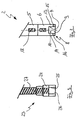
- the device 1 according to the invention shown in Fig. Has substantially the outer shape of an endoscope.
- the device 1 is equipped with an objective head 2, which contains a lens in a conventional manner, an eyepiece unit 3 and an image transfer unit 4 for transmitting the image received by the objective head 2 to the eyepiece unit 3.
- the image transfer unit 4 is arranged in a substantially tubular housing portion 5 of the device 1 and has a in the representation of FIG. 2 only schematically indicated glass fiber bundle 18, the optical head with the eyepiece unit 3 optically, that is image-transmitting coupled.
- a lens group may be arranged between the objective head and the eyepiece unit for transmitting and possibly enlarging the recorded image
- the objective head 2 which is shown enlarged in FIG. 2, has a housing 6, preferably made of stainless steel, which is funnel-shaped in cross-section (see FIG.
- the housing 6 is provided with a recess 7 which is formed in the representation of FIG. 2 is substantially square.
- the recess 7 is both down, that is to the axially outer end 8 of the device 1 out as well as laterally, that is in the illustration of FIG. 1 to the viewer out, open.
- a deflection prism 9 is arranged so that the free prism surface 10 to the outside (in the illustration of FIG. 1 to the left) and a deflection or deflection of the beam path by 90 degrees from the eyepiece unit 3 and the lens head formed vertical axis 11 takes place in the horizontal axis 12 and vice versa.
- the recess 7 is bounded laterally by two flange-like webs 13 and 14. On the one hand, these webs serve to fix and protect the deflecting prism 9 against mechanical damage and, on the other hand, light exits 15 and 16, which are part of a lighting device, are arranged in the axially outer ends of the webs 13 and 14.
- the light exits 15 and 16 are formed in this embodiment by the free axial ends of each of a fiber optic bundle, which are guided through the lens head 2 and the housing portion 5 to a fiber optic connector 17 which serves to feed the light of a light source, not shown, so that both light exits 15 and 16 are fed by the same light source.
- the glass fiber bundles are oriented in the region of the light exits so that the exit angle of the light is substantially equal to the deflection angle of the image deflection, whereby the entire optically achievable field of view can be illuminated without any vertical shading.
- the device 1 according to the invention, more precisely the lens head 2 as intended placed on a board or held at a small distance above the board surface.
- an electronic component 20 in the form of a BGA (Ball Grid Array) is fixed by soldering over the solder joints 21 in a known manner.
- the gap 22 between the component bottom and the board surface typically has between 0.02 and 0.8 mm gap height.
- the provisions of the Ablenkprismas 9 directly to the axially outermost distal end of the lens head 2 thessenaustritts- or image entry point of the prism and thus the lens can be placed in the gap area in total, whereby the gap and thus the arranged inside solder joints are optically accessible, which also due to the light emission at substantially the same axial height above the board surface as the image exit or image entry point sufficient illumination and thus good observability in the gap area is ensured.
- the illustrated in Fig. 1 embodiment of a device 1 according to the invention is further equipped with a backlight head 23.
- the backlight head 23 has a housing 24 (see FIG. 3) which is provided in a manner analogous to the housing 6 of the objective head 2 with a recess 25 and a deflection prism 26 arranged therein as described above for the objective head 2.
- the deflection prism 26 is optically not connected to the eyepiece unit 3, but rather via a glass fiber bundle 27, which is guided in a flexible spiral tube 28, in particular stainless steel, with the fiber optic connector 17 and thus the same light source, not shown
- the deflection prism 26 serves essentially to direct the introduction of backlight into the gap 22, which direction is essentially directed toward the objective head 2.
- a cantilevered support 29 is attached to the device 1.
- a groove-like guide 30 is formed in the carrier 29, in which a clamping piece 31 axially, that is guided in the axial direction of the carrier 29, slidably and clampable fixable.
- the clamping piece 31 extending in the spiral tube 28 glass fiber bundle 27 is held so that with the displacement of the clamping piece 30 at the same time the backlight head 23 slidably in the arrow direction and thus the exact distance of the backlight head 23 and lens head 2 in particular adapting to different sized BGA construction parts adjustable is.
- the support may be adjustable in height relative to the housing section 5 and rotatable by at least 90 ° to the support and thus to bring the backlight head from the working position to a rest position, if this is not needed, and vice versa.
- the device 1 In the area of the eyepiece unit 3, the device 1 is provided with a focus 32 for focusing the optical image. Furthermore, a video objective 33 is optically coupled to the eyepiece unit 3 in order to supply the recorded slit image to optical image processing or image storage. Further, a TV zoom adapter may be disposed between the camera and the eyepiece unit to correspondingly enlarge the transmitted image.
Claims (21)
- Dispositif d'inspection optique en particulier de liaisons brasées (21) cachées, en particulier entre d'une part un composant (20) électrique ou électronique, disposé sur la surface d'un circuit imprimé (19), et d'autre part ce circuit imprimé (19), avec une unité d'oculaire (3), une tête d'objectif (2), une unité de transmission d'image (4) pour transmettre l'image captée par la tête d'objectif (2) à l'unité d'oculaire (3), et une unité d'illumination (15, 16) pour illuminer les liaisons brasées (21) à examiner, la tête d'objectif (2) présentant un dispositif de déviation d'image (9) s'étendant jusqu'à la terminaison axialement extrême de la tête d'objectif (2), et le dispositif d'illumination (15, 16) étant disposé dans la tête d'objectif (2) de manière que l'angle de sortie de la lumière du dispositif d'illumination (15, 16) hors de la tête d'objectif (2) soit sensiblement égal à l'angle de déviation du dispositif de déviation d'image (9), et le site de sortie de la lumière est disposé sur le côté du dispositif de déviation d'image (9), dans la zone de la terminaison axialement extrême de la tête d'objectif (2).
- Dispositif selon la revendication 1, caractérisé en ce que la sortie (15, 16) de la lumière du dispositif d'illumination hors de la tête d'objectif (2) se fait des deux côtés, à côté du dispositif de déviation d'image (9).
- Dispositif selon la revendication 1 ou 2, caractérisé en ce que le dispositif de déviation d'image présente au moins un prisme de déviation (9), ou au moins un miroir de déviation.
- Dispositif selon l'une des revendications 1 à 3, caractérisé en ce que l'angle de déviation du dispositif de déviation d'image (9) est compris entre 0 et 180 degrés, de préférence est sensiblement de 90 degrés.
- Dispositif selon l'une des revendications 1 à 4, caractérisé en ce que l'objectif est conçu de manière que, en particulier présente une distance focale telle que, la plage de profondeur de champ de l'image correspond au moins à la moitié de la taille du composant.
- Dispositif selon l'une des revendications 1 à 5, caractérisé en ce que la tête d'objectif (2) présente un boîtier (6) avec au moins un évidement (7) ouvert latéralement et allant jusqu'à la terminaison axialement extrême de la tête d'objectif (2), évidement délimité des deux côtés par des nervures (13, 14) formant flasque, le prisme de déviation (9) ou le miroir de déviation étant disposé dans le boîtier (6), de manière que la surface libre (10) du prisme de déviation (9) ou la surface réfléchissante dans l'évidement (7) soit tournée vers l'extérieur et que l'arête latérale inférieure du prisme de déviation (9) ou du miroir de déviation délimite la tête d'objectif (2) à la terminaison axialement extrême (8) et en outre, les sorties de lumière (15, 16) du dispositif d'illumination étant disposées dans les nervures (13, 14) formant flasque.
- Dispositif selon l'une des revendications 1 à 6, caractérisé en ce que le dispositif d'illumination (15, 16) présente au moins un faisceau de fibres de verre qui peut être raccordé, par sa première extrémité axiale, à une source de lumière, et qui forme, avec sa deuxième extrémité axiale, la sortie de lumière (15, 16) du dispositif d'illumination sur la tête d'objectif (2).
- Dispositif selon l'une des revendications 1 à 7, caractérisé en ce que l'unité de transmission d'image (4) présente au moins un faisceau de fibres de verre (18) qui peut être couplé optiquement, par sa première extrémité, à l'unité de déviation d'image, en particulier le prisme de déviation (9) et, par sa deuxième extrémité, à l'unité d'oculaire (3).
- Dispositif selon l'une des revendications 1 à 8, caractérisé par un deuxième dispositif d'illumination, pouvant être positionné sensiblement en face de la tête d'objectif (2) dans la direction d'observation du dispositif (1) et illuminant dans la direction allant vers la tête d'objectif (2).
- Dispositif selon la revendication 9, caractérisé en ce que le deuxième dispositif d'illumination présente une tête de contre-éclairage (23) avec un boîtier (24), ayant au moins un évidement (25) ouvert latéralement et allant jusqu'à la terminaison axialement extrême de la tête de contre-éclairage (23), un prisme de déviation (26) ou un miroir de déviation, pouvant être couplé optiquement à une source lumineuse par un faisceau de fibres de verre (27), étant disposé dans le boîtier (24), de manière que la surface libre du prisme de déviation (26) ou la surface réfléchissante dans l'évidement (25) soit tournée vers l'extérieur, et l'arête latérale inférieure du prisme de déviation (26) ou du miroir de déviation délimitant la tête de contre-éclairage (23) à la terminaison axialement extrême.
- Dispositif selon la revendication 9, caractérisé en ce que le deuxième dispositif d'illumination présente une tête de contre-éclairage (23) de conception sensiblement identique à la tête d'objectif (2).
- Dispositif selon l'une des revendications 9 à 11, caractérisé en ce que le faisceau de fibres de verre (27) au moins du deuxième dispositif d'illumination s'étend dans un tuyau flexible à hélice (28).
- Dispositif selon l'une des revendications 9 à 12, caractérisé en ce que les faisceaux de fibres de verre de la tête d'objectif (2) et de la tête de contre-éclairage (23) peuvent être raccordés à la même source de lumière.
- Dispositif selon l'une des revendications 1 à 13, caractérisé en ce que le premier et/ou le deuxième dispositif d'illumination ou la source de lumière du premier ou deuxième dispositif d'illumination peuvent être réglés quant à leur intensité d'illumination ou intensité de lumière.
- Dispositif selon l'une des revendications 9 à 14, caractérisé en ce que la tête d'objectif (2) et le deuxième dispositif d'illumination sont susceptibles d'être couplés au moyen d'une tringlerie, d'un bâti ou analogue, de manière à pouvoir régler une position relative définie précisément de la tête d'objectif (2) et du deuxième dispositif d'illumination, en particulier de la tête de contre-éclairage (23).
- Dispositif selon la revendication 15, caractérisé en ce que la tringlerie ou le bâti présente un support (29), susceptible d'être fixé pratiquement rigidement, en étant en porte-à-faux libre sur un tronçon de boîtier (5) du dispositif (1), entre la tête d'objectif (2) et l'unité d'oculaire (3), ou fait partie de ce tronçon de boîtier (5), le support (29) présentant un élément support (31) déplaçable en direction longitudinale dans un guidage (30), dans lequel le deuxième dispositif d'illumination peut être fixé, avec lequel l'espacement axial, entre la tête d'objectif (2) et la tête de contre-éclairage (23), peut être réglé.
- Dispositif selon l'une des revendications 1 à 16, caractérisé en ce qu'un dispositif d'enregistrement d'image, de conversion d'image et/ou de traitement d'image, de nature électronique, optique ou magnétique, peut être couplé dans la zone de l'unité d'oculaire (3) en transmettant l'image directement ou indirectement.
- Procédé d'examen de la qualité de la liaison brasée entre d'une part un composant électrique ou électronique disposé sur la surface d'un circuit imprimé ou analogue, et d'autre part ce circuit imprimé, avec utilisation du dispositif selon l'une des revendications précédentes, le composant présentant une pluralité de pattes de brasage, de billes de brasage ou de points de brasage, disposées à la façon d'une matrice, en rangées et en colonnes, pouvant être brasé(e)s avec un nombre correspondant de points de contact disposés sur le circuit imprimé, de façon complémentaire du point de vue de la forme et de la fonction, avec les étapes de procédé suivantes :a) examen optique des liaisons brasées de la rangée la plus extérieure des liaisons brasées d'un premier côté du composant à examiner, le composant étant passé pas à pas, de manière correspondante à l'espacement des rangées ou des colonnes de points de brasage, sur la tête d'objectif du dispositif ou bien, à l'inverse, la tête d'objectif du dispositif étant passée pas à pas sur le composant ;b) rotation du composant et du dispositif chaque fois de 90 degrés et examen optique, de façon analogue à l'étape de procédé a), des liaisons brasées des rangées les plus extérieures des liaisons brasées des autres côtés du composant ; etc) examen optique des canaux chaque fois formés entre les colonnes ou les rangées, pour vérifier qu'ils sont dégagés.
- Procédé selon la revendication 18, caractérisé en ce que le composant électrique ou électronique est un SMD ou BGA.
- Procédé selon l'une des revendications 18 et 19, caractérisé en ce que l'étape de procédé c) est conduite en contre-éclairage.
- Procédé selon la revendication 18, 19 ou 20, caractérisé en ce que, en plus des étapes de procédé a) et b), on examine, de façon simultanée ou temporellement décalée, la liaison brasée des rangées intérieures, par inspection optique dans les canaux formés entre les colonnes ou les rangées, pour détecter les défauts de brasure.
Applications Claiming Priority (3)
| Application Number | Priority Date | Filing Date | Title |
|---|---|---|---|
| DE19847913 | 1998-10-19 | ||
| DE19847913A DE19847913B4 (de) | 1998-10-19 | 1998-10-19 | Vorrichtung und Verfahren zur optischen Inspektion insbesondere verdeckter Lötverbindungen |
| PCT/DE1999/002617 WO2000023844A1 (fr) | 1998-10-19 | 1999-08-20 | Dispositif et procede pour l'examen optique de brasures cachees |
Publications (3)
| Publication Number | Publication Date |
|---|---|
| EP1123525A1 EP1123525A1 (fr) | 2001-08-16 |
| EP1123525B1 EP1123525B1 (fr) | 2002-07-24 |
| EP1123525B2 true EP1123525B2 (fr) | 2007-02-14 |
Family
ID=7884793
Family Applications (1)
| Application Number | Title | Priority Date | Filing Date |
|---|---|---|---|
| EP99953551A Expired - Lifetime EP1123525B2 (fr) | 1998-10-19 | 1999-08-20 | Dispositif et procede pour l'examen optique de brasures cachees |
Country Status (16)
| Country | Link |
|---|---|
| US (1) | US6580501B2 (fr) |
| EP (1) | EP1123525B2 (fr) |
| JP (1) | JP4030693B2 (fr) |
| KR (1) | KR100620448B1 (fr) |
| CN (1) | CN1166973C (fr) |
| AT (1) | ATE221210T1 (fr) |
| AU (1) | AU752862B2 (fr) |
| BR (1) | BR9913735A (fr) |
| CA (1) | CA2346914C (fr) |
| DE (2) | DE19847913B4 (fr) |
| DK (1) | DK1123525T4 (fr) |
| ES (1) | ES2178485T5 (fr) |
| HK (1) | HK1039521B (fr) |
| MX (1) | MXPA01002436A (fr) |
| PT (1) | PT1123525E (fr) |
| WO (1) | WO2000023844A1 (fr) |
Families Citing this family (15)
| Publication number | Priority date | Publication date | Assignee | Title |
|---|---|---|---|---|
| JP4063469B2 (ja) * | 2000-03-10 | 2008-03-19 | 株式会社ハイロックス | 超微小空隙から内部を観察するための装置 |
| KR100454216B1 (ko) * | 2001-10-22 | 2004-10-26 | 한전기공주식회사 | 측정게이지 조명장치 |
| US6788406B2 (en) * | 2001-11-02 | 2004-09-07 | Delaware Capital Formation, Inc. | Device and methods of inspecting soldered connections |
| US6847900B2 (en) * | 2001-12-17 | 2005-01-25 | Agilent Technologies, Inc. | System and method for identifying solder joint defects |
| US7231833B2 (en) | 2003-04-01 | 2007-06-19 | Intel Corporation | Board deflection metrology using photoelectric amplifiers |
| JP3953988B2 (ja) * | 2003-07-29 | 2007-08-08 | Tdk株式会社 | 検査装置および検査方法 |
| US7356936B1 (en) | 2004-01-14 | 2008-04-15 | Honda Motor Co., Ltd. | Apparatus and method for measuring coating accumulations in a spray booth |
| DE102006003931B3 (de) | 2006-01-26 | 2007-08-02 | Infineon Technologies Ag | Halbleiterbauteil mit oberflächenmontierbaren Außenkontakten und Verfahren zur Herstellung desselben |
| US7643136B2 (en) * | 2006-02-02 | 2010-01-05 | Optilia Instrument Ab | Device for inspection of narrow spaces and objects in narrow spaces |
| US8068228B2 (en) | 2007-08-07 | 2011-11-29 | Nanometrics Incorporated | In-plane optical metrology |
| EA020561B1 (ru) * | 2009-12-04 | 2014-12-30 | Баррик Гольд Корпорейшн | Выделение минералов меди из пирита с использованием аэрирования и метабисульфитной обработки |
| CN102183357B (zh) * | 2010-10-21 | 2012-11-14 | 中国人民银行印制科学技术研究所 | 防伪元件隐藏图像明暗区域对比度的检测方法与装置 |
| JP6242078B2 (ja) | 2013-05-20 | 2017-12-06 | オリンパス株式会社 | 半導体装置、および半導体装置の位置決め装置 |
| CN104283144A (zh) * | 2013-07-01 | 2015-01-14 | 北京电研华源电力技术有限公司 | 一种观测环网柜隔离开关断口的方法及装置 |
| CN105826787B (zh) * | 2016-05-09 | 2018-08-28 | 莱芜钢铁集团有限公司 | 滑线巡点检用工具 |
Citations (5)
| Publication number | Priority date | Publication date | Assignee | Title |
|---|---|---|---|---|
| US4699463A (en) † | 1985-11-01 | 1987-10-13 | Circon Corporation | Multidirectional viewing borescope |
| JPH0242213A (ja) † | 1988-06-22 | 1990-02-13 | Valeo | ねじり緩衝装置 |
| JPH0447255A (ja) † | 1990-06-15 | 1992-02-17 | Hitachi Ltd | 電子部品の微細接続検査装置 |
| US5295477A (en) † | 1992-05-08 | 1994-03-22 | Parviz Janfaza | Endoscopic operating microscope |
| JPH06244600A (ja) † | 1993-02-20 | 1994-09-02 | Tdk Corp | 集積回路チップ浮き上がり検査装置 |
Family Cites Families (21)
| Publication number | Priority date | Publication date | Assignee | Title |
|---|---|---|---|---|
| DE7440701U (de) | 1975-04-30 | Richard Wolf Gmbh | Endoskop, insbesondere Laryngoskop und Epipharyngoskop | |
| US3021834A (en) * | 1954-03-11 | 1962-02-20 | Sheldon Edward Emanuel | Endoscopes |
| JPS5389451A (en) * | 1977-01-18 | 1978-08-07 | Olympus Optical Co Ltd | Endoscope visual field direction changing attachment optical system |
| JPS54154759U (fr) * | 1978-04-20 | 1979-10-27 | ||
| JPS60247106A (ja) * | 1984-05-22 | 1985-12-06 | Fujitsu Ltd | 形状検査装置 |
| US4727859A (en) * | 1986-12-29 | 1988-03-01 | Welch Allyn, Inc. | Right angle detachable prism assembly for borescope |
| US4846154A (en) * | 1988-06-13 | 1989-07-11 | Macanally Richard B | Dual view endoscope |
| JPH03215704A (ja) * | 1990-01-19 | 1991-09-20 | Fujitsu Ltd | バンプ検査装置 |
| JPH0452614A (ja) * | 1990-06-20 | 1992-02-20 | Olympus Optical Co Ltd | 内視鏡 |
| US5052802A (en) * | 1990-07-24 | 1991-10-01 | Hewlett-Packard Company | Device for viewing beneath circuit boards |
| JPH0690362B2 (ja) * | 1991-04-08 | 1994-11-14 | 三菱電線工業株式会社 | ファイバスコープ |
| JPH0694429A (ja) * | 1991-06-24 | 1994-04-05 | Mitsubishi Electric Corp | 表面実装部品半田付外観検査方法 |
| DE4207874C2 (de) * | 1992-03-12 | 2002-12-12 | Fraunhofer Ges Forschung | Visuelle Kontrolleinrichtung |
| DE4304422C1 (de) * | 1993-02-13 | 1994-07-21 | Winter & Ibe Olympus | Endoskop |
| US5613936A (en) * | 1995-02-22 | 1997-03-25 | Concurrent Technologies Corp. | Stereo laparoscope apparatus |
| US5644438A (en) * | 1995-10-30 | 1997-07-01 | Pottash; Paul C. | Optical device for viewing into restricted areas |
| DE29603327U1 (de) * | 1996-02-16 | 1996-04-18 | Schich Gisbert | Endoskop zur Rohrinnenwandprüfung |
| DE19830710B4 (de) * | 1997-08-01 | 2010-10-28 | Carl Zeiss | Endoskop |
| KR100278477B1 (ko) * | 1997-10-24 | 2001-03-02 | 윤종용 | 광학현미경 |
| DE29805624U1 (de) * | 1998-03-27 | 1998-06-04 | Drendel Andrea | Beleuchtung für Staboptikendoskope und flexible Glasfaserendoskope in medizinischen und technischen Bereichen |
| DE29806922U1 (de) * | 1998-04-17 | 1998-06-18 | Schich Gisbert | Endoskop mit zwei Blickrichtungen |
-
1998
- 1998-10-19 DE DE19847913A patent/DE19847913B4/de not_active Expired - Lifetime
-
1999
- 1999-08-20 KR KR1020017004264A patent/KR100620448B1/ko not_active IP Right Cessation
- 1999-08-20 ES ES99953551T patent/ES2178485T5/es not_active Expired - Lifetime
- 1999-08-20 WO PCT/DE1999/002617 patent/WO2000023844A1/fr active IP Right Grant
- 1999-08-20 CN CNB998121738A patent/CN1166973C/zh not_active Expired - Fee Related
- 1999-08-20 AU AU10277/00A patent/AU752862B2/en not_active Ceased
- 1999-08-20 PT PT99953551T patent/PT1123525E/pt unknown
- 1999-08-20 AT AT99953551T patent/ATE221210T1/de active
- 1999-08-20 EP EP99953551A patent/EP1123525B2/fr not_active Expired - Lifetime
- 1999-08-20 DK DK99953551T patent/DK1123525T4/da active
- 1999-08-20 DE DE59902144T patent/DE59902144D1/de not_active Expired - Lifetime
- 1999-08-20 CA CA002346914A patent/CA2346914C/fr not_active Expired - Fee Related
- 1999-08-20 MX MXPA01002436A patent/MXPA01002436A/es active IP Right Grant
- 1999-08-20 BR BR9913735-6A patent/BR9913735A/pt not_active Application Discontinuation
- 1999-09-10 JP JP25741599A patent/JP4030693B2/ja not_active Expired - Fee Related
-
2001
- 2001-05-25 US US09/866,400 patent/US6580501B2/en not_active Expired - Fee Related
-
2002
- 2002-02-21 HK HK02101279.8A patent/HK1039521B/zh not_active IP Right Cessation
Patent Citations (5)
| Publication number | Priority date | Publication date | Assignee | Title |
|---|---|---|---|---|
| US4699463A (en) † | 1985-11-01 | 1987-10-13 | Circon Corporation | Multidirectional viewing borescope |
| JPH0242213A (ja) † | 1988-06-22 | 1990-02-13 | Valeo | ねじり緩衝装置 |
| JPH0447255A (ja) † | 1990-06-15 | 1992-02-17 | Hitachi Ltd | 電子部品の微細接続検査装置 |
| US5295477A (en) † | 1992-05-08 | 1994-03-22 | Parviz Janfaza | Endoscopic operating microscope |
| JPH06244600A (ja) † | 1993-02-20 | 1994-09-02 | Tdk Corp | 集積回路チップ浮き上がり検査装置 |
Non-Patent Citations (1)
| Title |
|---|
| MINISKOP Serie PKF 07/93 † |
Also Published As
| Publication number | Publication date |
|---|---|
| CA2346914A1 (fr) | 2000-04-27 |
| KR20010085882A (ko) | 2001-09-07 |
| HK1039521A1 (en) | 2002-04-26 |
| US6580501B2 (en) | 2003-06-17 |
| US20010024273A1 (en) | 2001-09-27 |
| DE19847913A1 (de) | 1999-05-06 |
| DE19847913B4 (de) | 2005-09-22 |
| ES2178485T5 (es) | 2007-10-01 |
| JP4030693B2 (ja) | 2008-01-09 |
| DE59902144D1 (de) | 2002-08-29 |
| KR100620448B1 (ko) | 2006-09-05 |
| ATE221210T1 (de) | 2002-08-15 |
| PT1123525E (pt) | 2002-11-29 |
| HK1039521B (zh) | 2005-04-29 |
| CN1323407A (zh) | 2001-11-21 |
| AU1027700A (en) | 2000-05-08 |
| MXPA01002436A (es) | 2002-05-08 |
| WO2000023844A1 (fr) | 2000-04-27 |
| AU752862B2 (en) | 2002-10-03 |
| CA2346914C (fr) | 2008-02-05 |
| DK1123525T3 (da) | 2002-11-11 |
| CN1166973C (zh) | 2004-09-15 |
| DK1123525T4 (da) | 2007-04-02 |
| BR9913735A (pt) | 2001-06-05 |
| EP1123525A1 (fr) | 2001-08-16 |
| EP1123525B1 (fr) | 2002-07-24 |
| ES2178485T3 (es) | 2002-12-16 |
| JP2000131029A (ja) | 2000-05-12 |
Similar Documents
| Publication | Publication Date | Title |
|---|---|---|
| EP1123525B2 (fr) | Dispositif et procede pour l'examen optique de brasures cachees | |
| DE4342654C2 (de) | Prüfvorrichtung zum Prüfen gedruckter Leiterplatten | |
| DE69832940T2 (de) | Beobachtungsgerät und Gerät zum Verschmelzungsspleissen von optischen Fasern | |
| DE102004029212B4 (de) | Vorrichtung und Verfahren zur optischen Auf- und/oder Durchlichtinspektion von Mikrostrukturen im IR | |
| DE3537995A1 (de) | Endoskop | |
| DE2930407A1 (de) | Geraet zur untersuchung von rohren in einer anlage | |
| EP0842633A1 (fr) | Endoscope électronique utilisé entièrement dans un autoclave | |
| DE102008009975B4 (de) | Vorrichtung zur Abbildung der Innenfläche einer Bohrung in einem Werkstück | |
| DE102005012127A1 (de) | Foto-Erfassungseinrichtung und diese verwendende Temperaturverteilungs-Erfassungseinrichtung | |
| EP3162273A1 (fr) | Instrument médical optique | |
| EP2818094B1 (fr) | Instrument d'observation équipé d'un champ d'image symétrique en utilisant des capteurs d'image asymétriques | |
| DE19646236C2 (de) | Vorrichtung zur endoskopischen Diagnose und Behandlung von Gewebe | |
| DE19654208C2 (de) | Mikroskop | |
| DE2244441C3 (de) | Verfahren zum Betrieb eines Korpuskularstrahlgerätes | |
| EP3254148A2 (fr) | Endoscope | |
| EP1443352A1 (fr) | Arrangement optique destiné à étre connecté à un microscope pour la mesure de mouvements d'une microstructure | |
| EP3714759B1 (fr) | Procédé de fabrication d'un endoscope | |
| DE10249669B3 (de) | Verfahren zur Bestimmung der relativen räumlichen Lage zwischen zwei Kameras und Kamera zum optischen Erfassen von Objekten | |
| DE4214968C2 (de) | Vorrichtung zur Bilderkennung | |
| DE112020004901T5 (de) | Endoskop und endoskopvorrichtung | |
| DE102014107586A1 (de) | 3D-Video-Endoskop | |
| DE102007040488A1 (de) | Röntgeneinrichtung | |
| DE10135320A1 (de) | Mikroskopobjektiv und Verwendung eines solchen Mikroskopobjektivs bei einem Mikroskop | |
| DE102019130950B3 (de) | Boroskop mit Musterprojektion | |
| EP2229584A1 (fr) | Sonde et dispositif pour la vérification optique d'objets à mesurer |
Legal Events
| Date | Code | Title | Description |
|---|---|---|---|
| PUAI | Public reference made under article 153(3) epc to a published international application that has entered the european phase |
Free format text: ORIGINAL CODE: 0009012 |
|
| 17P | Request for examination filed |
Effective date: 20001110 |
|
| AK | Designated contracting states |
Kind code of ref document: A1 Designated state(s): AT BE CH CY DE DK ES FI FR GB GR IE IT LI LU MC NL PT SE |
|
| AX | Request for extension of the european patent |
Free format text: AL;LT;LV;MK;RO;SI |
|
| GRAG | Despatch of communication of intention to grant |
Free format text: ORIGINAL CODE: EPIDOS AGRA |
|
| GRAG | Despatch of communication of intention to grant |
Free format text: ORIGINAL CODE: EPIDOS AGRA |
|
| GRAH | Despatch of communication of intention to grant a patent |
Free format text: ORIGINAL CODE: EPIDOS IGRA |
|
| 17Q | First examination report despatched |
Effective date: 20020121 |
|
| GRAH | Despatch of communication of intention to grant a patent |
Free format text: ORIGINAL CODE: EPIDOS IGRA |
|
| GRAA | (expected) grant |
Free format text: ORIGINAL CODE: 0009210 |
|
| AK | Designated contracting states |
Kind code of ref document: B1 Designated state(s): AT BE CH CY DE DK ES FI FR GB GR IE IT LI LU MC NL PT SE |
|
| PG25 | Lapsed in a contracting state [announced via postgrant information from national office to epo] |
Ref country code: GR Free format text: LAPSE BECAUSE OF FAILURE TO SUBMIT A TRANSLATION OF THE DESCRIPTION OR TO PAY THE FEE WITHIN THE PRESCRIBED TIME-LIMIT Effective date: 20020724 |
|
| REF | Corresponds to: |
Ref document number: 221210 Country of ref document: AT Date of ref document: 20020815 Kind code of ref document: T |
|
| REG | Reference to a national code |
Ref country code: GB Ref legal event code: FG4D Free format text: NOT ENGLISH |
|
| REG | Reference to a national code |
Ref country code: CH Ref legal event code: EP |
|
| REG | Reference to a national code |
Ref country code: CH Ref legal event code: NV Representative=s name: MANFRED SAEGER PATENTANWALT |
|
| PG25 | Lapsed in a contracting state [announced via postgrant information from national office to epo] |
Ref country code: LU Free format text: LAPSE BECAUSE OF NON-PAYMENT OF DUE FEES Effective date: 20020820 |
|
| REG | Reference to a national code |
Ref country code: IE Ref legal event code: FG4D Free format text: GERMAN |
|
| REF | Corresponds to: |
Ref document number: 59902144 Country of ref document: DE Date of ref document: 20020829 |
|
| PG25 | Lapsed in a contracting state [announced via postgrant information from national office to epo] |
Ref country code: CY Free format text: LAPSE BECAUSE OF FAILURE TO SUBMIT A TRANSLATION OF THE DESCRIPTION OR TO PAY THE FEE WITHIN THE PRESCRIBED TIME-LIMIT Effective date: 20020831 |
|
| GBT | Gb: translation of ep patent filed (gb section 77(6)(a)/1977) |
Effective date: 20020919 |
|
| REG | Reference to a national code |
Ref country code: DK Ref legal event code: T3 |
|
| REG | Reference to a national code |
Ref country code: PT Ref legal event code: SC4A Free format text: AVAILABILITY OF NATIONAL TRANSLATION Effective date: 20020924 |
|
| REG | Reference to a national code |
Ref country code: ES Ref legal event code: FG2A Ref document number: 2178485 Country of ref document: ES Kind code of ref document: T3 |
|
| ET | Fr: translation filed | ||
| PG25 | Lapsed in a contracting state [announced via postgrant information from national office to epo] |
Ref country code: MC Free format text: LAPSE BECAUSE OF NON-PAYMENT OF DUE FEES Effective date: 20030301 |
|
| PLBQ | Unpublished change to opponent data |
Free format text: ORIGINAL CODE: EPIDOS OPPO |
|
| PLBQ | Unpublished change to opponent data |
Free format text: ORIGINAL CODE: EPIDOS OPPO |
|
| PLBI | Opposition filed |
Free format text: ORIGINAL CODE: 0009260 |
|
| PLBQ | Unpublished change to opponent data |
Free format text: ORIGINAL CODE: EPIDOS OPPO |
|
| PLBI | Opposition filed |
Free format text: ORIGINAL CODE: 0009260 |
|
| PLBF | Reply of patent proprietor to notice(s) of opposition |
Free format text: ORIGINAL CODE: EPIDOS OBSO |
|
| 26 | Opposition filed |
Opponent name: METCAL, INC. Effective date: 20030423 Opponent name: KEYMED (MEDICAL & INDUSTRIAL EQUIPMENT) LIMITE Effective date: 20030422 |
|
| 26 | Opposition filed |
Opponent name: TECHNOLAB GMBH Effective date: 20030423 Opponent name: METCAL, INC. Effective date: 20030423 Opponent name: KEYMED (MEDICAL & INDUSTRIAL EQUIPMENT) LIMITE Effective date: 20030422 |
|
| NLR1 | Nl: opposition has been filed with the epo |
Opponent name: TECHNOLAB GMBH Opponent name: METCAL, INC. Opponent name: KEYMED (MEDICAL & INDUSTRIAL EQUIPMENT) LIMITED |
|
| PLAX | Notice of opposition and request to file observation + time limit sent |
Free format text: ORIGINAL CODE: EPIDOSNOBS2 |
|
| PLBQ | Unpublished change to opponent data |
Free format text: ORIGINAL CODE: EPIDOS OPPO |
|
| PLAB | Opposition data, opponent's data or that of the opponent's representative modified |
Free format text: ORIGINAL CODE: 0009299OPPO |
|
| PLBB | Reply of patent proprietor to notice(s) of opposition received |
Free format text: ORIGINAL CODE: EPIDOSNOBS3 |
|
| R26 | Opposition filed (corrected) |
Opponent name: TECHNOLAB GMBH Effective date: 20030423 Opponent name: METCAL, INC. Effective date: 20030423 Opponent name: KEYMED (MEDICAL & INDUSTRIAL EQUIPMENT) LIMITE Effective date: 20030422 |
|
| NLR1 | Nl: opposition has been filed with the epo |
Opponent name: TECHNOLAB GMBH Opponent name: METCAL, INC. Opponent name: KEYMED (MEDICAL & INDUSTRIAL EQUIPMENT) LIMITED |
|
| PLCK | Communication despatched that opposition was rejected |
Free format text: ORIGINAL CODE: EPIDOSNREJ1 |
|
| APBP | Date of receipt of notice of appeal recorded |
Free format text: ORIGINAL CODE: EPIDOSNNOA2O |
|
| APBM | Appeal reference recorded |
Free format text: ORIGINAL CODE: EPIDOSNREFNO |
|
| APBQ | Date of receipt of statement of grounds of appeal recorded |
Free format text: ORIGINAL CODE: EPIDOSNNOA3O |
|
| PLAQ | Examination of admissibility of opposition: information related to despatch of communication + time limit deleted |
Free format text: ORIGINAL CODE: EPIDOSDOPE2 |
|
| PLAR | Examination of admissibility of opposition: information related to receipt of reply deleted |
Free format text: ORIGINAL CODE: EPIDOSDOPE4 |
|
| PLBQ | Unpublished change to opponent data |
Free format text: ORIGINAL CODE: EPIDOS OPPO |
|
| PLAB | Opposition data, opponent's data or that of the opponent's representative modified |
Free format text: ORIGINAL CODE: 0009299OPPO |
|
| R26 | Opposition filed (corrected) |
Opponent name: TECHNOLAB GMBH Effective date: 20030423 Opponent name: METCAL, INC. Effective date: 20030423 Opponent name: KEYMED (MEDICAL & INDUSTRIAL EQUIPMENT) LIMITE Effective date: 20030422 |
|
| NLR1 | Nl: opposition has been filed with the epo |
Opponent name: TECHNOLAB GMBH Opponent name: METCAL, INC. Opponent name: KEYMED (MEDICAL & INDUSTRIAL EQUIPMENT) LIMITED |
|
| APAH | Appeal reference modified |
Free format text: ORIGINAL CODE: EPIDOSCREFNO |
|
| PLBP | Opposition withdrawn |
Free format text: ORIGINAL CODE: 0009264 |
|
| PLAB | Opposition data, opponent's data or that of the opponent's representative modified |
Free format text: ORIGINAL CODE: 0009299OPPO |
|
| APBU | Appeal procedure closed |
Free format text: ORIGINAL CODE: EPIDOSNNOA9O |
|
| R26 | Opposition filed (corrected) |
Opponent name: TECHNOLAB GMBH Effective date: 20030423 Opponent name: KEYMED (MEDICAL & INDUSTRIAL EQUIPMENT) LIMITED Effective date: 20030422 |
|
| NLR1 | Nl: opposition has been filed with the epo |
Opponent name: TECHNOLAB GMBH Opponent name: KEYMED (MEDICAL & INDUSTRIAL EQUIPMENT) LIMITED |
|
| PUAH | Patent maintained in amended form |
Free format text: ORIGINAL CODE: 0009272 |
|
| STAA | Information on the status of an ep patent application or granted ep patent |
Free format text: STATUS: PATENT MAINTAINED AS AMENDED |
|
| REG | Reference to a national code |
Ref country code: SE Ref legal event code: RPOT |
|
| 27A | Patent maintained in amended form |
Effective date: 20070214 |
|
| AK | Designated contracting states |
Kind code of ref document: B2 Designated state(s): AT BE CH CY DE DK ES FI FR GB GR IE IT LI LU MC NL PT SE |
|
| REG | Reference to a national code |
Ref country code: CH Ref legal event code: AEN Free format text: AUFRECHTERHALTUNG DES PATENTES IN GEAENDERTER FORM |
|
| NLR2 | Nl: decision of opposition |
Effective date: 20070214 |
|
| REG | Reference to a national code |
Ref country code: DK Ref legal event code: T4 |
|
| GBTA | Gb: translation of amended ep patent filed (gb section 77(6)(b)/1977) |
Effective date: 20070321 |
|
| REG | Reference to a national code |
Ref country code: SE Ref legal event code: RPEO |
|
| NLR3 | Nl: receipt of modified translations in the netherlands language after an opposition procedure | ||
| ET3 | Fr: translation filed ** decision concerning opposition | ||
| REG | Reference to a national code |
Ref country code: ES Ref legal event code: DC2A Date of ref document: 20070425 Kind code of ref document: T5 |
|
| REG | Reference to a national code |
Ref country code: CH Ref legal event code: PCAR Free format text: MANFRED SAEGER;POSTFACH 5;7304 MAIENFELD (CH) |
|
| PLAB | Opposition data, opponent's data or that of the opponent's representative modified |
Free format text: ORIGINAL CODE: 0009299OPPO |
|
| REG | Reference to a national code |
Ref country code: CH Ref legal event code: PFA Owner name: ERSA GMBH Free format text: ERSA GMBH#LEONHARD-KARL-STRASSE 24#97877 WERTHEIM (DE) -TRANSFER TO- ERSA GMBH#LEONHARD-KARL-STRASSE 24#97877 WERTHEIM (DE) |
|
| PLAB | Opposition data, opponent's data or that of the opponent's representative modified |
Free format text: ORIGINAL CODE: 0009299OPPO |
|
| REG | Reference to a national code |
Ref country code: CH Ref legal event code: PCAR Free format text: NEW ADDRESS: FELDGUEETLIWEG 130, 8706 MEILEN (CH) |
|
| PGFP | Annual fee paid to national office [announced via postgrant information from national office to epo] |
Ref country code: PT Payment date: 20130220 Year of fee payment: 15 Ref country code: DK Payment date: 20130819 Year of fee payment: 15 Ref country code: FI Payment date: 20130821 Year of fee payment: 15 Ref country code: IE Payment date: 20130819 Year of fee payment: 15 Ref country code: ES Payment date: 20130828 Year of fee payment: 15 Ref country code: NL Payment date: 20130822 Year of fee payment: 15 Ref country code: CH Payment date: 20130826 Year of fee payment: 15 Ref country code: AT Payment date: 20130821 Year of fee payment: 15 Ref country code: SE Payment date: 20130822 Year of fee payment: 15 |
|
| PGFP | Annual fee paid to national office [announced via postgrant information from national office to epo] |
Ref country code: FR Payment date: 20130820 Year of fee payment: 15 Ref country code: GB Payment date: 20130823 Year of fee payment: 15 |
|
| PGFP | Annual fee paid to national office [announced via postgrant information from national office to epo] |
Ref country code: IT Payment date: 20130823 Year of fee payment: 15 |
|
| PGFP | Annual fee paid to national office [announced via postgrant information from national office to epo] |
Ref country code: DE Payment date: 20131022 Year of fee payment: 15 Ref country code: BE Payment date: 20130821 Year of fee payment: 15 |
|
| REG | Reference to a national code |
Ref country code: PT Ref legal event code: MM4A Free format text: LAPSE DUE TO NON-PAYMENT OF FEES Effective date: 20150220 |
|
| REG | Reference to a national code |
Ref country code: DE Ref legal event code: R119 Ref document number: 59902144 Country of ref document: DE |
|
| REG | Reference to a national code |
Ref country code: NL Ref legal event code: V1 Effective date: 20150301 |
|
| REG | Reference to a national code |
Ref country code: DK Ref legal event code: EBP Effective date: 20140831 |
|
| REG | Reference to a national code |
Ref country code: CH Ref legal event code: PL Ref country code: SE Ref legal event code: EUG |
|
| REG | Reference to a national code |
Ref country code: AT Ref legal event code: MM01 Ref document number: 221210 Country of ref document: AT Kind code of ref document: T Effective date: 20140820 |
|
| GBPC | Gb: european patent ceased through non-payment of renewal fee |
Effective date: 20140820 |
|
| PG25 | Lapsed in a contracting state [announced via postgrant information from national office to epo] |
Ref country code: NL Free format text: LAPSE BECAUSE OF NON-PAYMENT OF DUE FEES Effective date: 20150301 Ref country code: FI Free format text: LAPSE BECAUSE OF NON-PAYMENT OF DUE FEES Effective date: 20140820 Ref country code: IT Free format text: LAPSE BECAUSE OF NON-PAYMENT OF DUE FEES Effective date: 20140820 Ref country code: LI Free format text: LAPSE BECAUSE OF NON-PAYMENT OF DUE FEES Effective date: 20140831 Ref country code: CH Free format text: LAPSE BECAUSE OF NON-PAYMENT OF DUE FEES Effective date: 20140831 Ref country code: BE Free format text: LAPSE BECAUSE OF NON-PAYMENT OF DUE FEES Effective date: 20140831 Ref country code: PT Free format text: LAPSE BECAUSE OF NON-PAYMENT OF DUE FEES Effective date: 20150220 |
|
| REG | Reference to a national code |
Ref country code: IE Ref legal event code: MM4A |
|
| REG | Reference to a national code |
Ref country code: DE Ref legal event code: R119 Ref document number: 59902144 Country of ref document: DE Effective date: 20150303 |
|
| PG25 | Lapsed in a contracting state [announced via postgrant information from national office to epo] |
Ref country code: AT Free format text: LAPSE BECAUSE OF NON-PAYMENT OF DUE FEES Effective date: 20140820 Ref country code: SE Free format text: LAPSE BECAUSE OF NON-PAYMENT OF DUE FEES Effective date: 20140821 |
|
| REG | Reference to a national code |
Ref country code: FR Ref legal event code: ST Effective date: 20150430 |
|
| PG25 | Lapsed in a contracting state [announced via postgrant information from national office to epo] |
Ref country code: GB Free format text: LAPSE BECAUSE OF NON-PAYMENT OF DUE FEES Effective date: 20140820 Ref country code: DK Free format text: LAPSE BECAUSE OF NON-PAYMENT OF DUE FEES Effective date: 20140831 Ref country code: DE Free format text: LAPSE BECAUSE OF NON-PAYMENT OF DUE FEES Effective date: 20150303 |
|
| PG25 | Lapsed in a contracting state [announced via postgrant information from national office to epo] |
Ref country code: IE Free format text: LAPSE BECAUSE OF NON-PAYMENT OF DUE FEES Effective date: 20140820 Ref country code: FR Free format text: LAPSE BECAUSE OF NON-PAYMENT OF DUE FEES Effective date: 20140901 |
|
| REG | Reference to a national code |
Ref country code: ES Ref legal event code: FD2A Effective date: 20150925 |
|
| PG25 | Lapsed in a contracting state [announced via postgrant information from national office to epo] |
Ref country code: ES Free format text: LAPSE BECAUSE OF NON-PAYMENT OF DUE FEES Effective date: 20140821 |