EP1123525B2 - Device and method for the optical inspection of concealed soldered connections - Google Patents
Device and method for the optical inspection of concealed soldered connections Download PDFInfo
- Publication number
- EP1123525B2 EP1123525B2 EP99953551A EP99953551A EP1123525B2 EP 1123525 B2 EP1123525 B2 EP 1123525B2 EP 99953551 A EP99953551 A EP 99953551A EP 99953551 A EP99953551 A EP 99953551A EP 1123525 B2 EP1123525 B2 EP 1123525B2
- Authority
- EP
- European Patent Office
- Prior art keywords
- head
- lens head
- image
- illuminating device
- lens
- Prior art date
- Legal status (The legal status is an assumption and is not a legal conclusion. Google has not performed a legal analysis and makes no representation as to the accuracy of the status listed.)
- Expired - Lifetime
Links
Images

Classifications
-
- G—PHYSICS
- G01—MEASURING; TESTING
- G01B—MEASURING LENGTH, THICKNESS OR SIMILAR LINEAR DIMENSIONS; MEASURING ANGLES; MEASURING AREAS; MEASURING IRREGULARITIES OF SURFACES OR CONTOURS
- G01B11/00—Measuring arrangements characterised by the use of optical techniques
- G01B11/30—Measuring arrangements characterised by the use of optical techniques for measuring roughness or irregularity of surfaces
-
- G—PHYSICS
- G01—MEASURING; TESTING
- G01M—TESTING STATIC OR DYNAMIC BALANCE OF MACHINES OR STRUCTURES; TESTING OF STRUCTURES OR APPARATUS, NOT OTHERWISE PROVIDED FOR
- G01M11/00—Testing of optical apparatus; Testing structures by optical methods not otherwise provided for
- G01M11/08—Testing mechanical properties
- G01M11/081—Testing mechanical properties by using a contact-less detection method, i.e. with a camera
-
- G—PHYSICS
- G01—MEASURING; TESTING
- G01N—INVESTIGATING OR ANALYSING MATERIALS BY DETERMINING THEIR CHEMICAL OR PHYSICAL PROPERTIES
- G01N21/00—Investigating or analysing materials by the use of optical means, i.e. using sub-millimetre waves, infrared, visible or ultraviolet light
- G01N21/84—Systems specially adapted for particular applications
- G01N21/88—Investigating the presence of flaws or contamination
- G01N21/8806—Specially adapted optical and illumination features
-
- H—ELECTRICITY
- H05—ELECTRIC TECHNIQUES NOT OTHERWISE PROVIDED FOR
- H05K—PRINTED CIRCUITS; CASINGS OR CONSTRUCTIONAL DETAILS OF ELECTRIC APPARATUS; MANUFACTURE OF ASSEMBLAGES OF ELECTRICAL COMPONENTS
- H05K13/00—Apparatus or processes specially adapted for manufacturing or adjusting assemblages of electric components
- H05K13/08—Monitoring manufacture of assemblages
- H05K13/081—Integration of optical monitoring devices in assembly lines; Processes using optical monitoring devices specially adapted for controlling devices or machines in assembly lines
- H05K13/0817—Monitoring of soldering processes
Definitions
- the invention relates to a device for optical inspection in particular concealed solder joints according to the preamble of patent claim 1.
- the invention relates to a method according to claim 16.
- solder joints non-destructively by means of X-rays.
- this known method only unwanted short-circuiting solder bridges between adjacent pins or the correct position of the pins of the components at the contact points of the board can ultimately be checked; a statement about the quality of the individual solder joints or the optical quality of the surface of the individual solder joints or, for example, unwanted flux residues in the soldering is not possible.
- such systems are very expensive to buy and maintain and the application of this known method with respect to radiation exposure is not entirely safe.
- such systems can only be operated by highly qualified specialist personnel.
- Another known method for determining the quality of a solder joint is the production of a microsection in cross section through the respective solder joint.
- reliable statements about the quality of the solder joint for example a sufficient melting of the solder point of the component and thus a satisfactory wetting of the contact point on the board, can be made, but this is a destructive test method that can only be used randomly, to allow conclusions about the process parameters of the soldering process.
- an optical control of the surface of the individual solder joints is also not possible here.
- endoscopes with lighting devices are known with which inaccessible spaces are optically controllable.
- the known endoscopes have a substantially tubular construction, at the axially outer end of a deflection unit is arranged with illumination, which deflects the light exit from the tubular structure in the gap direction or the slit image in the direction of the eyepiece. Due to their design, however, the insight into gaps of low height, in particular in the range below 1 mm gap height, as is the case in particular with BGAs and other SMDs, is not possible.
- the device for optical inspection of hidden solder joints in particular between an electrical or electronic soldered on a board component, such as a BGA, and the board for checking the quality of the solder joint, first an eyepiece, a lens head, an image transmission unit for transmitting the lens head taken on the eyepiece unit and a lighting device for illuminating the examined solder joints.
- the device according to the invention initially has the basic design of a technical or medical endoscope.
- a device for image deflection is provided in a manner also known per se in the region of the objective head.
- the means for image deflection to the axially outer end of the lens head In contrast to the known endoscopes, however, in which the lens or the deflection by design has at least a small distance from the axially outer "distal" end of the lens head extends in the apparatus according to the invention the means for image deflection to the axially outer end of the lens head.
- the illumination device or the light exit is arranged above or below the lens or the deflection unit, whereby the optically achievable gap height increases and / or an undesirable light shadow is generated in the gap region
- the illumination device according to the invention arranged in the lens head such that the exit angle of the light of the illumination device from the lens head is substantially equal to the deflection angle of the image deflection and the exit location of the light next to the device for image deflection in the region of the axially outer end of the lens head.
- the illumination device is arranged at substantially the same height, based on the board surface or cleavage plane, as the image exit or image entry point of the lens and on the other hand, the image illumination without any vertical shading occurs.
- solder joints in columns with a height of less than 1 mm and significantly below.
- the individual solder joints for example in the case of BGAs, CSPs and FCs, which as a rule have a gap height of approximately 0.02 to 0.8 mm between the underside of the component and the board, are optically non-destructive of soldering defects, unwanted bridging, impurities and the like are controllable.
- the exit of the light of the illumination device can be made on one side of the objective head. According to a preferred embodiment of the invention, however, the exit of the light of the illumination device from the lens head takes place on both sides next to the device for image deflection, whereby a uniform illumination of the field of view is ensured.
- the deflection or deflection of the image in the objective head from the direction of the object to be observed in the direction of the eyepiece can likewise be effected in any desired manner, for example in the simplest case by means of a deflecting mirror.
- the device for image deflection preferably has a deflection prism, in which the deflection takes place in a manner known per se. This can be compared to the mirror deflection in particular the optical quality of the image improves and in particular the Jardinaulingers- or image entry point of the lens to further down, that is placed in the direction of the axially outer end of the lens head.
- the deflection angle of the device for image deflection is basically arbitrary and can be between 0 and 180 degrees.
- the deflection angle depends essentially on the angle at which the endoscope of the device is raised relative to the surface of the board.
- the deflection angle is substantially 90 degrees. That is, in other words, that the device according to this embodiment of the invention, based on the optical axis between the lens and eyepiece is substantially perpendicular to the board and thus set to the cleavage plane.
- the device can be used even with tightly populated boards and thus relatively narrow spaces between the components to be tested for application.
- the lens is designed so that the depth of field of the figure or the focal length of at least half the size of the component, for example, half the component width, half Component length or half the component diameter corresponds.
- the entire gap interior can be optically controlled.
- the depth of field range of the lens can be preset in a conventional manner, for example, by the focal length of the lens.
- the lens head has a housing with at least one laterally open and expiring toward the axially outer end of the lens head recess, which is bounded on both sides by flange-like webs on.
- the deflection prism or the deflection mirror is arranged in this housing such that the free, that is, the gap facing surface of the Ablenkprismas or the mirror surface in the recess to the outside, based on the housing and the recess, and the lower side edge the Ablenkprismas or the deflection mirror closes the lens head to the axially outer end.
- the lower end of the deflection prism or the deflection mirror can be brought directly to the board to ensure image deflection in the lowest column, while the side edges of the prism or the mirror through the flange-like webs against damage be protected and at the same time the prism or the mirror is fixed by these webs.
- the light exits of the illumination device can be arranged in the flange-like webs.
- the illumination device has at least one glass fiber bundle, which can be connected with its first axial end to a light source, be it externally or in or on the device, and with its second axial end the light exit of the illumination device on the objective head forms.
- a glass fiber bundle in particular a light exit can be realized in a simple manner, which with sufficient illuminance a sufficiently small diameter to illuminate a narrow gap. If two or more light exits are present in the lens head, the respective glass fiber bundles between light exit and light source can be combined into a bundle and fed to a common light source.
- the transmission of the slit image from the objective head to the eyepiece can take place, for example, by means of a lens or mirror system.
- the device according to the invention for image transmission has at least one further fiber optic bundle, which is optically coupled with its first end to the image deflection unit, in particular the deflection prism, and with its second end to the eyepiece.
- a second illumination device is provided according to a particularly preferred embodiment of the invention, which can be positioned opposite the lens head relative to the objective head and illuminates in the direction of the objective head, essentially in view or in the direction of the image, with reference to the cleavage plane. This can be in a simple way when looking through the gap spaces between the rows of solder points by detecting the backlight source exclude a shorting bridge and, conversely, unambiguously determine an unwanted bridge, if the backlight source is not visible.
- the second illumination device has a backlight head with a housing having at least one laterally open and expiring towards the axially outer end of the backlight head recess, wherein in the housing a Ablenkprisma or a deflection mirror or via a glass fiber bundle to a Light source is connected, is arranged such that the free surface of the Ablenkprismas or the mirror surface in the recess facing outward and the lower side edge of the Ablenkprismas or the AblenkLites the light head to the axially outer end closes.
- the second illumination device may have a backlight head which is constructed substantially identical to the objective head of the device.
- the backlight head and the lens head can each serve simultaneously as a lighting device and / or imager, simultaneously or alternately, so that simultaneously or alternately, the gap can be controlled by both sides of a BGA, for example.
- the prism of the backlight head can be switchably connected to the eyepiece of the lens head or optically coupled with a separate eyepiece.
- the glass fiber bundle of at least the second illumination device can run in a flexible spiral hose.
- the glass fiber bundle is reliably protected against mechanical damage and, on the other hand, this makes it possible to adjust the backlight head in adaptation to BGAs of different dimensions, in particular in its distance from the objective head.
- the illumination device of the backlight head and the illumination device of the objective head can be coupled in any way to different light sources.
- the glass fiber bundles of the lens head and the backlight head are connectable to the same light source. This results in a total of a simple and inexpensive structural design.
- the first and / or the second illumination device or the light source of the first and / or second illumination device can be adjustable in their luminous intensity or light intensity.
- the objective head can be illuminated by the backlight source.
- the objective head and the second illumination device can be coupled via a linkage, frame or the like in such a way that a precisely defined relative position of the objective head and illumination device, in particular the backlight head, can be set.
- the linkage or frame on a support which cantilevering on a housing portion of the device between the lens head and eyepiece is substantially rigidly fastened or part of this housing portion.
- the carrier has a longitudinally displaceable in a guide member, in which the second illumination device is directly or indirectly fixed and with the particular axial distance between the lens head and the backlight head is adjustable on.
- an electronically, magnetically or optically image-recording, image-converting and / or image-processing device can be coupled directly or indirectly in the region of the eyepiece.
- This can be, for example, a video or television camera, the CCD image converter is directly or indirectly connected via a corresponding lens to the eyepiece.
- the thus recorded video image can be placed on a screen and / or subjected to image processing in a computer. This makes it possible to automate the inspection of solder joints under a BGA in basically any way, for example by comparing images with reference images.
- the gap height can also be determined and measured and optionally compared with a critical gap height.
- the device according to the invention can be arranged in a manner known per se on an XY table, on which a board-component solder joint to be examined is brought into the test position under the device or, conversely, the device is brought into the test position over the board-Bautell solder joint can be.
- the process steps a) to c) do not necessarily have to be performed chronologically in this order. Rather, in particular the method step c) can be carried out simultaneously with the method steps a) and b) during the stepwise passage of the component on the objective head or, conversely, the objective head on the component.
- the method step c) is performed in the backlight, resulting in a particularly easy and quick recognition of unwanted shorting bridges.
- the solder joints of the inner rows by looking into the channels formed between the columns or rows optically be examined for soldering defects.
- co-planarity errors between the component and the board in the gap interior can be determined easily and reliably.
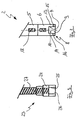
- the device 1 according to the invention shown in Fig. Has substantially the outer shape of an endoscope.
- the device 1 is equipped with an objective head 2, which contains a lens in a conventional manner, an eyepiece unit 3 and an image transfer unit 4 for transmitting the image received by the objective head 2 to the eyepiece unit 3.
- the image transfer unit 4 is arranged in a substantially tubular housing portion 5 of the device 1 and has a in the representation of FIG. 2 only schematically indicated glass fiber bundle 18, the optical head with the eyepiece unit 3 optically, that is image-transmitting coupled.
- a lens group may be arranged between the objective head and the eyepiece unit for transmitting and possibly enlarging the recorded image
- the objective head 2 which is shown enlarged in FIG. 2, has a housing 6, preferably made of stainless steel, which is funnel-shaped in cross-section (see FIG.
- the housing 6 is provided with a recess 7 which is formed in the representation of FIG. 2 is substantially square.
- the recess 7 is both down, that is to the axially outer end 8 of the device 1 out as well as laterally, that is in the illustration of FIG. 1 to the viewer out, open.
- a deflection prism 9 is arranged so that the free prism surface 10 to the outside (in the illustration of FIG. 1 to the left) and a deflection or deflection of the beam path by 90 degrees from the eyepiece unit 3 and the lens head formed vertical axis 11 takes place in the horizontal axis 12 and vice versa.
- the recess 7 is bounded laterally by two flange-like webs 13 and 14. On the one hand, these webs serve to fix and protect the deflecting prism 9 against mechanical damage and, on the other hand, light exits 15 and 16, which are part of a lighting device, are arranged in the axially outer ends of the webs 13 and 14.
- the light exits 15 and 16 are formed in this embodiment by the free axial ends of each of a fiber optic bundle, which are guided through the lens head 2 and the housing portion 5 to a fiber optic connector 17 which serves to feed the light of a light source, not shown, so that both light exits 15 and 16 are fed by the same light source.
- the glass fiber bundles are oriented in the region of the light exits so that the exit angle of the light is substantially equal to the deflection angle of the image deflection, whereby the entire optically achievable field of view can be illuminated without any vertical shading.
- the device 1 according to the invention, more precisely the lens head 2 as intended placed on a board or held at a small distance above the board surface.
- an electronic component 20 in the form of a BGA (Ball Grid Array) is fixed by soldering over the solder joints 21 in a known manner.
- the gap 22 between the component bottom and the board surface typically has between 0.02 and 0.8 mm gap height.
- the provisions of the Ablenkprismas 9 directly to the axially outermost distal end of the lens head 2 thessenaustritts- or image entry point of the prism and thus the lens can be placed in the gap area in total, whereby the gap and thus the arranged inside solder joints are optically accessible, which also due to the light emission at substantially the same axial height above the board surface as the image exit or image entry point sufficient illumination and thus good observability in the gap area is ensured.
- the illustrated in Fig. 1 embodiment of a device 1 according to the invention is further equipped with a backlight head 23.
- the backlight head 23 has a housing 24 (see FIG. 3) which is provided in a manner analogous to the housing 6 of the objective head 2 with a recess 25 and a deflection prism 26 arranged therein as described above for the objective head 2.
- the deflection prism 26 is optically not connected to the eyepiece unit 3, but rather via a glass fiber bundle 27, which is guided in a flexible spiral tube 28, in particular stainless steel, with the fiber optic connector 17 and thus the same light source, not shown
- the deflection prism 26 serves essentially to direct the introduction of backlight into the gap 22, which direction is essentially directed toward the objective head 2.
- a cantilevered support 29 is attached to the device 1.
- a groove-like guide 30 is formed in the carrier 29, in which a clamping piece 31 axially, that is guided in the axial direction of the carrier 29, slidably and clampable fixable.
- the clamping piece 31 extending in the spiral tube 28 glass fiber bundle 27 is held so that with the displacement of the clamping piece 30 at the same time the backlight head 23 slidably in the arrow direction and thus the exact distance of the backlight head 23 and lens head 2 in particular adapting to different sized BGA construction parts adjustable is.
- the support may be adjustable in height relative to the housing section 5 and rotatable by at least 90 ° to the support and thus to bring the backlight head from the working position to a rest position, if this is not needed, and vice versa.
- the device 1 In the area of the eyepiece unit 3, the device 1 is provided with a focus 32 for focusing the optical image. Furthermore, a video objective 33 is optically coupled to the eyepiece unit 3 in order to supply the recorded slit image to optical image processing or image storage. Further, a TV zoom adapter may be disposed between the camera and the eyepiece unit to correspondingly enlarge the transmitted image.
Abstract
Description
Die Erfindung betrifft eine Vorrichtung zur optischen Inspektion insbesondere verdeckter Lötverbindungen nach dem Oberbegriff des Patentanspruchs 1.The invention relates to a device for optical inspection in particular concealed solder joints according to the preamble of patent claim 1.
Weiter betrifft die Erfindung ein Verfahren nach dem Patentanspruch 16.Furthermore, the invention relates to a method according to
Im Bereich der Löttechnologie, insbesondere bei der Verwendung von SMDs (Surface Mounted Devices), und hier wiederum insbesondere bei sogenannten BGAs (Ball Grid Arrays), CSPs (Chip Scale Pakkages) und FCs (Flip Chips) tritt das Problem auf, daß aufgrund der geringen Spalthöhe zwischen der Unterseite der Bauelemente und der Platine die Qualität der Lötverbindung sowohl der außen als auch der innen liegenden Pin-Reihen zu den entsprechenden Kontaktpunkten der Platine durch bloße Inaugenscheinnahme nicht mehr kontrollierbar ist. Daher werden die entsprechenden elektrischen bzw. elektronischen Bauteile bzw. Baugruppen nach dem Löten im allgemeinen einer elektrischen Funktionsprüfung unterzogen. Dies ist zum einen jedoch zeitaufwendig und damit teuer und kann zum anderen nur eine Aussage darüber liefern, ob die Lötverbindungen stromdurchgängig bzw. ob Kurzschlüsse vorhanden sind. Eine Aussage über die Qualität und damit Dauerhaftigkeit bzw die zu erwartende Lebensdauer der einzelnen Lötverbindungen kann dieses Testverfahren nicht liefern.In the field of soldering technology, in particular in the use of SMDs (Surface Mounted Devices), and here again in particular in so-called BGAs (Ball Grid Arrays), CSPs (Chip Scale Pakkages) and FCs (Flip Chips), the problem arises that due to the low gap height between the bottom of the components and the board, the quality of the solder joint of both the outside and the inside pin rows to the corresponding contact points of the board by mere inspection is no longer controllable. Therefore, the corresponding electrical or electronic components or assemblies are subjected after soldering in general an electrical functional test. On the one hand, however, this is time-consuming and therefore expensive and, on the other hand, can only provide information about whether the soldered connections are current-continuous or whether short-circuits exist. A statement about the quality and thus durability or the expected lifetime of the individual solder joints can not provide this test method.
Es ist ferner bekannt, Lötverbindungen zerstörungsfrei mittels Röntgenstrahlen zu überprüfen. Auch bei diesem bekannten Verfahren können letztlich nur unerwünschte einen Kurzschluß verursachende Lötbrücken zwischen benachbarten Pins bzw. die richtige Position der Pins der Bau - elemente auf den Kontaktpunkten der Platine überprüft werden; eine Aussage über die Qualität der einzelnen Lötverbindungen bzw die optische Qualität der Oberfläche der einzelnen Lötverbindungen oder beispielsweise über unerwünschte Flußmittelrückstände im Bereich der Lötungen ist nicht möglich. Zudem sind derartige Anlagen in Anschaffung und Unterhalt sehr kostspielig und die Anwendung dieses bekannten Verfahrens im Hinblick auf Strahlenbelastungen nicht ganz unbedenklich. Zudem können derartige Anlagen nur von hochqualifiziertem Fachpersonal bedient werden.It is also known to test solder joints non-destructively by means of X-rays. In the case of this known method as well, only unwanted short-circuiting solder bridges between adjacent pins or the correct position of the pins of the components at the contact points of the board can ultimately be checked; a statement about the quality of the individual solder joints or the optical quality of the surface of the individual solder joints or, for example, unwanted flux residues in the soldering is not possible. In addition, such systems are very expensive to buy and maintain and the application of this known method with respect to radiation exposure is not entirely safe. In addition, such systems can only be operated by highly qualified specialist personnel.
Ein weiteres bekanntes Verfahren zur Bestimmung der Qualität einer Lötverbindung ist die Herstellung eines Schliffbildes im Querschnitt durch die jeweilige Lötverbindung. Damit können zwar zuverlässige Aussagen über die Qualität der Lötverbindung, beispielsweise eine ausreichende Aufschmelzung des Lotpunktes des Bauteils und damit eine zufriedenstellende Benetzung des Kontaktpunktes auf der Platine, getroffen werden, doch handelt es sich hierbei um ein zerstörendes Prüfverfahren, das lediglich stichprobenartig Verwendung finden kann, um Rückschlüsse auf die Verfahrensparameter des Lötprozesses zu ermöglichen. Zudem ist auch hierbei eine optische Kontrolle der Oberfläche der einzelnen Lötverbindungen nicht möglich.Another known method for determining the quality of a solder joint is the production of a microsection in cross section through the respective solder joint. Thus, although reliable statements about the quality of the solder joint, for example a sufficient melting of the solder point of the component and thus a satisfactory wetting of the contact point on the board, can be made, but this is a destructive test method that can only be used randomly, to allow conclusions about the process parameters of the soldering process. In addition, an optical control of the surface of the individual solder joints is also not possible here.
Schließlich sind aus dem Bereich der Medizin und der Technik Endoskope mit Beleuchtungseinrichtungen bekannt, mit denen unzugängliche Räume optisch kontrollierbar sind. Die bekannten Endoskope weisen einen im wesentlichen rohrförmigen Aufbau auf, an dessen axial äußeren Ende eine Ablenkeinheit mit Beleuchtung angeordnet ist, die den Lichtaustritt aus dem rohrförmigen Aufbau in Spaltrichtung bzw das Spaltbild in Richtung des Okulars umlenkt. Aufgrund ihrer Bauart ist jedoch der Einblick in Spalte geringer Höhe, insbesondere im Bereich unter 1 mm Spalthöhe, wie dies insbesondere bei BGAs und anderen SMDs regelmäßig der Fall ist, nicht möglich.Finally, from the field of medicine and technology endoscopes with lighting devices are known with which inaccessible spaces are optically controllable. The known endoscopes have a substantially tubular construction, at the axially outer end of a deflection unit is arranged with illumination, which deflects the light exit from the tubular structure in the gap direction or the slit image in the direction of the eyepiece. Due to their design, however, the insight into gaps of low height, in particular in the range below 1 mm gap height, as is the case in particular with BGAs and other SMDs, is not possible.
Ausgehend von diesem Stand der Technik ist es die Aufgabe der vorliegenden Erfindung, eine gattungsgemäße Vorrichtung zu schaffen, die in vergleichsweise einfacher und kostengünstiger Weise zerstörungsfrei die optische Inspektion insbesondere verdeckter Lötstellen ermöglicht.Based on this prior art, it is the object of the present invention to provide a generic device that enables non-destructive optical inspection in particular concealed solder joints in a relatively simple and cost-effective manner.
Diese Aufgabe wird durch eine Vorrichtung nach der Lehre des Anspruchs 1 gelöst.This object is achieved by a device according to the teaching of claim 1.
Es ist ferner eine weitere Aufgabe der Erfindung, eine Verfahren zu liefern, mit dem in einfacher Weise die Qualität einer Lötverbindung zwischen einem auf der Oberfläche einer Platine oder dergleichen angeordnetem elektrischen oder elektronischen Bauteil, insbesondere einem SMD- oder BGA-Bauteil, und der Platine überprüfbar ist.It is a further object of the invention to provide a method with which easily the quality of a solder joint between an arranged on the surface of a board or the like electrical or electronic component, in particular an SMD or BGA component, and the board is verifiable.
Vorteilhafte Ausgestaltungen der Erfindung sind Gegenstand der Unteransprüche.Advantageous embodiments of the invention are the subject of the dependent claims.
Erfindungsgemäß weist die Vorrichtung zur optischen Inspektion verdeckter Lötstellen, insbesondere zwischen einem elektrischen oder elektronischen auf einer Platine verlöteten Bauteil, beispielsweise einem BGA, und der Platine zur Überprüfung der Qualität der Lötverbindung, zunächst eine Okulareinheit, einen Objektivkopf, eine Bildübertragungseinheit zur Übertragung des vom Objektivkopf aufgenommenen Bildes an die Okulareinheit und eine Beleuchtungseinrichtung zur Beleuchtung der zu untersuchenden Lötverbindungen auf. Mit anderen Worten, die erfindungsgemäße Vorrichtung weist zunächst die grundsätzliche Bauweise eines technischen oder medizinischen Endoskops auf. Weiter ist in zunächst ebenfalls für sich bekannter Weise im Bereich des Objektivkopfs eine Einrichtung zur Bildablenkung vorgesehen.According to the invention, the device for optical inspection of hidden solder joints, in particular between an electrical or electronic soldered on a board component, such as a BGA, and the board for checking the quality of the solder joint, first an eyepiece, a lens head, an image transmission unit for transmitting the lens head taken on the eyepiece unit and a lighting device for illuminating the examined solder joints. In other words, the device according to the invention initially has the basic design of a technical or medical endoscope. Furthermore, a device for image deflection is provided in a manner also known per se in the region of the objective head.
Im Gegensatz zu den bekannten Endoskopen jedoch, bei denen das Objektiv bzw. die Ablenkung bauartbedingt einen zumindest geringen Abstand vom axial äußeren "distalen" Ende des Objektivkopfs aufweist, erstreckt sich bei der erfindungsgemäßen Vorrichtung die Einrichtung zur Bildablenkung bis zum axial äußeren Ende des Objektivkopfs. Bereits dadurch läßt sich der Bildaustritts- bzw- Bildeintrittspunkt des Objektives im Vergleich zum Stand derTechnik erheblich näher an die Platine legen, so daß Spalten geringerer Höhe bzw. darin angeordnete Lötstellen optisch inspizierbar sind.In contrast to the known endoscopes, however, in which the lens or the deflection by design has at least a small distance from the axially outer "distal" end of the lens head extends in the apparatus according to the invention the means for image deflection to the axially outer end of the lens head. Already as a result, the Bildaustritts- or image entry point of the lens in comparison to the state of the art can be significantly closer to the board, so that columns of lesser height or therein arranged solder joints are optically inspectable.
Ebenfalls im Gegensatz zu den bekannten Endoskopen, bei denen die Beleuchtungseinrichtung bzw. der Lichtaustritt über oder unter dem Objektiv bzw. der Ablenkeinheit angeordnet ist, wodurch die optisch zu erreichende Spalthöhe vergrößert und/oder ein unerwünschter Lichtschatten im Spaltbereich erzeugt wird, ist erfindungsgemäß die Beleuchtungseinrichtung im Objektivkopf derart angeordnet, daß der Austrittswinkel des Lichtes der Beleuchtungseinrichtung aus dem Objektivkopf im wesentlichen gleich dem Ablenkwinkel der Bildablenkung ist und der Austrittsort des Lichtes neben der Einrichtung zur Bildablenkung im Bereich des axial äußeren Endes des Objektivkopfs angeordnet. Dies bedeutet mit anderen Worten, daß zum einen die Beleuchtungseinrichtung im wesentlichen in der gleichen Höhe, bezogen auf die Platinenoberfläche oder Spaltebene, angeordnet ist wie der Bildaustritts- bzw. Bildeintrittspunkt des Objektives und zum anderen die Bildausleuchtung ohne jegliche vertikale Abschattung erfolgt.Also in contrast to the known endoscopes, in which the illumination device or the light exit is arranged above or below the lens or the deflection unit, whereby the optically achievable gap height increases and / or an undesirable light shadow is generated in the gap region, the illumination device according to the invention arranged in the lens head such that the exit angle of the light of the illumination device from the lens head is substantially equal to the deflection angle of the image deflection and the exit location of the light next to the device for image deflection in the region of the axially outer end of the lens head. This means, in other words, that on the one hand, the illumination device is arranged at substantially the same height, based on the board surface or cleavage plane, as the image exit or image entry point of the lens and on the other hand, the image illumination without any vertical shading occurs.
Insgesamt lassen sich mit der erfindungsgemäßen Vorrichtung in einfacher Weise Lötstellen in Spalten mit eine Höhe von unter 1 mm und deutlich darunter optisch inspizieren. Dies bedeutet insbesondere, daß damit die einzelnen Lötverbindungen beispielsweise bei BGAs, CSPs und FCs, die im Regelfall eine Spalthöhe von ca. 0,02 bis 0,8 mm zwischen Bauteilunterseite und Platine aufweisen, optisch auf Lötfehler, unerwünschte Brückenbildung, Verunreinigungen und dergleichen zerstörungsfrei kontrollierbar sind.Overall, can be optically inspect with the device according to the invention in a simple way solder joints in columns with a height of less than 1 mm and significantly below. This means, in particular, that the individual solder joints, for example in the case of BGAs, CSPs and FCs, which as a rule have a gap height of approximately 0.02 to 0.8 mm between the underside of the component and the board, are optically non-destructive of soldering defects, unwanted bridging, impurities and the like are controllable.
In grundsätzlich beliebiger Weise kann der Austritt des Lichtes der Beleuchtungseinrichtung einseitig am Objektivkopf erfolgen. Nach einem bevorzugten Ausführungsbeispiel der Erfindung jedoch erfolgt der Austritt des Lichtes der Beleuchtungseinrichtung aus dem Objektivkopf beidseitig neben der Einrichtung zur Bildablenkung, wodurch eine gleichmäßige Ausleuchtung des Blickfeldes sichergestellt ist.In basically any way, the exit of the light of the illumination device can be made on one side of the objective head. According to a preferred embodiment of the invention, however, the exit of the light of the illumination device from the lens head takes place on both sides next to the device for image deflection, whereby a uniform illumination of the field of view is ensured.
Die Ab- bzw. Umlenkung des Bildes im Objektivkopf aus Richtung des zu beobachtenden Objekts in Richtung des Okulars kann ebenfalls in beliebiger Weise erfolgen, beispielsweise im einfachsten Fall mittels eines Umlenkspiegels. Vorzugsweise jedoch weist die Einrichtung zur Bildablenkung ein Ablenkprisma auf, in dem in an sich bekannter Weise die Umlenkung erfolgt. Damit kann im Vergleich zur Spiegelumlenkung insbesondere die optische Qualität der Abbildung verbessert und insbesondere auch der Bildautritts- bzw. Bildeintrittspunkt des Objektivs nach weiter unten, das heißt in Richtung des axial äußeren Endes des Objektivkopfs gelegt werden.The deflection or deflection of the image in the objective head from the direction of the object to be observed in the direction of the eyepiece can likewise be effected in any desired manner, for example in the simplest case by means of a deflecting mirror. However, the device for image deflection preferably has a deflection prism, in which the deflection takes place in a manner known per se. This can be compared to the mirror deflection in particular the optical quality of the image improves and in particular the Bildautritts- or image entry point of the lens to further down, that is placed in the direction of the axially outer end of the lens head.
Der Ablenkwinkel der Einrichtung zur Bildablenkung ist grundsätzlich beliebigig und kann zwischen 0 und 180 Grad liegen. Dabei hängt der Ablenkwinkel im wesentlichen vom Winkel ab, in dem das Endoskop der Vorrichtung relativ zur Platinenoberfläche angestzt wird. Vorzugsweise beträgt der Ablenkwinkel im wesentlichen 90 Grad. Das heißt mit anderen Worten, daß die Vorrichtung gemäß diesem Ausführungsbeispiel der Erfindung, bezogen auf die optische Achse zwischen Objektiv und Okular im wesentlichen rechtwinklig zur Platine und damit zur Spaltebene angesetzt wird. Damit läßt sich die Vorrichtung auch bei eng bestückten Platinen und damit vergleichsweise engen Zwischenräumen zwischen den zu prüfenden Bauteilen zur Anwendung bringen.The deflection angle of the device for image deflection is basically arbitrary and can be between 0 and 180 degrees. In this case, the deflection angle depends essentially on the angle at which the endoscope of the device is raised relative to the surface of the board. Preferably, the deflection angle is substantially 90 degrees. That is, in other words, that the device according to this embodiment of the invention, based on the optical axis between the lens and eyepiece is substantially perpendicular to the board and thus set to the cleavage plane. Thus, the device can be used even with tightly populated boards and thus relatively narrow spaces between the components to be tested for application.
Insbesondere wenn nicht nur die äußeren Lötverbindungen im Kantenbereich des Bauteils überprüft werden sollen, ist nach einem weiteren besonders bevorzugten Ausführungsbeispiel der Erfindung das Objektiv derart ausgelegt, daß der Tiefenschärfenbereich der Abbildung bzw. die Brennweite mindestens der halben Bauteilgröße, beispielsweise der halben Bauteilbreite, der halben Bauteillänge oder dem halben Bauteildurchmesser entspricht. Dadurch kann durch Inspektion von jeweils gegenüberliegenden Seiten des Bauteils der gesamte Spaltinnenraum optisch kontrolliert werden. Der Tiefenschärfenbereich des Objektivs kann dabei in an sich bekannter Weise beispielsweise durch die Brennweite des Objektivs voreingestellt werden.In particular, when not only the outer solder joints are to be checked in the edge region of the component, according to a further particularly preferred embodiment of the invention, the lens is designed so that the depth of field of the figure or the focal length of at least half the size of the component, for example, half the component width, half Component length or half the component diameter corresponds. As a result, by inspection of respective opposite sides of the component, the entire gap interior can be optically controlled. The depth of field range of the lens can be preset in a conventional manner, for example, by the focal length of the lens.
Nach einem besonders bevorzugten Ausführungsbeispiel weist der Objektivkopf ein Gehäuse mit mindestens einer seitlich offenen und zum axial äußeren Ende des Objektivkopfs hin auslaufenden Ausnehmung, die beidseitig von flanschartigen Stegen begrenzt wird, auf. Dabei ist in diesem Gehäuse das Ablenkprisma bzw. der Ablenkspiegel derart angeordnet, daß die freie, das heißt die zum Spalt weisende Fläche des Ablenkprismas bzw. die Spiegelfläche in der Ausnehmung nach außen, bezogen auf das Gehäuse und die Ausnehmung, weist und die untere Seitenkante des Ablenkprismas bzw. des Ablenkspiegels den Objektivkopf zum axial äußeren Ende hin abschließt. Dies bedeutet mit anderen Worten, daß das untere Ende des Ablenkprismas bzw. des Ablenkspiegels unmittelbar zur Anlage an die Platine bringbar ist, um eine Bildumlenkung auch in niedrigste Spalte zu gewährleisten, während die Seitenkanten des Prismas bzw. des Spiegels durch die flanschartigen Stege gegen Beschädigung geschützt werden und gleichzeitig das Prisma bzw. der Spiegel durch diese Stege fixierbar ist. Bei diesem Ausführungsbeispiel können ferner die Lichtaustritte der Beleuchtungseinrichtung in den flanschartigen Stegen angeordnet sein.According to a particularly preferred embodiment, the lens head has a housing with at least one laterally open and expiring toward the axially outer end of the lens head recess, which is bounded on both sides by flange-like webs on. In this case, the deflection prism or the deflection mirror is arranged in this housing such that the free, that is, the gap facing surface of the Ablenkprismas or the mirror surface in the recess to the outside, based on the housing and the recess, and the lower side edge the Ablenkprismas or the deflection mirror closes the lens head to the axially outer end. This means in other words that the lower end of the deflection prism or the deflection mirror can be brought directly to the board to ensure image deflection in the lowest column, while the side edges of the prism or the mirror through the flange-like webs against damage be protected and at the same time the prism or the mirror is fixed by these webs. In this embodiment, furthermore, the light exits of the illumination device can be arranged in the flange-like webs.
Nach einem weiteren bevorzugten Ausführungsbeispiel weist die Beleuchtungseinrichtung mindestens ein Glasfaserbündel auf, das mit seinem ersten axialen Ende an eine Lichtquelle, sei diese nun extern oder aber in oder an der Vorrichtung angeordnet, anschließbar ist und mit seinem zweiten axialen Ende den Lichtaustritt der Beleuchtungseinrichtung am Objektivkopf bildet. Durch die Verwendung eines Glasfaserbündels kann in einfacher Weise insbesondere ein Lichtaustritt realisiert werden, der bei ausreichender Beleuchtungsstärke einen genügend kleinen Durchmesser zur Beleuchtung eines engen Spaltes aufweist. Falls zwei oder mehrere Lichtaustritte im Objektivkopf vorhanden sind, können die jeweiligen Glasfaserbündel zwischen Lichtaustritt und Lichtquelle zu einem Bündel zusammengefaßt und einer gemeinsamen Lichtquelle zugeführt werden.According to a further preferred embodiment, the illumination device has at least one glass fiber bundle, which can be connected with its first axial end to a light source, be it externally or in or on the device, and with its second axial end the light exit of the illumination device on the objective head forms. By using a glass fiber bundle, in particular a light exit can be realized in a simple manner, which with sufficient illuminance a sufficiently small diameter to illuminate a narrow gap. If two or more light exits are present in the lens head, the respective glass fiber bundles between light exit and light source can be combined into a bundle and fed to a common light source.
Die Übertragung des Spaltbildes vom Objektivkopf an das Okular kann beispielsweise durch ein Linsen- oder Spiegelsystem erfolgen. Vorzugsweise jedoch weist die erfindungsgemäße Vorrichtung zur Bildübertragung mindestens ein weiteres Glasfaserbündel, das mit seinem ersten Ende an die Einheit zur Bildablenkung, insbesondere das Ablenkprisma, und mit seinem zweiten Ende an das Okular optisch ankoppelbar ist.The transmission of the slit image from the objective head to the eyepiece can take place, for example, by means of a lens or mirror system. Preferably, however, the device according to the invention for image transmission has at least one further fiber optic bundle, which is optically coupled with its first end to the image deflection unit, in particular the deflection prism, and with its second end to the eyepiece.
Grundsätzlich lassen sich mit den vorstehend beschriebenen Ausführungsbeispielen alle Arten von Lötfehlern sowohl im Randbereich als auch, bei ausreichender Tiefenschärfe des Objektivs, im inneren Bereich des Lötfeldes beispielsweise eines BGA, eines CSP oder eines FC optisch kontrollieren und ermitteln. Insbesondere, jedoch keineswegs ausschließlich, wenn es darum geht, unerwünschte einen Kurzschluß verursachende Lötbrücken zwischen benachbarten "Lötpins" eines BGA, eines CSP oder eines FC mit einer Vielzahl von Lötpunkten zu entdecken, ist nach einem besonders bevorzugten Ausführungsbeispiel der Erfindung eine zweite Beleuchtungseinrichtung vorgesehen, die im wesentlichen in Blick- bzw. in Bildrichtung, bezogen auf die Spaltebene, der Vorrichtung dem Objektivkopf gegenüber positionierbar ist und in Richtung zum Objektivkopf leuchtet. Damit läßt sich in einfacher Weise beim Durchblick durch die Spaltzwischenräume zwischen den einzelnen Reihen der Lötpunkte durch Erkennen der Gegenlichtquelle eine Kurzschlußbrücke ausschließen und, umgekehrt, in eindeutiger Weise eine unerwünschte Brücke ermitteln, falls die Gegenlichtquelle nicht zu sehen ist.In principle, all types of soldering errors can be visually checked and determined both in the edge region and, with sufficient depth of focus of the objective, in the inner region of the solder field, for example, a BGA, a CSP or a FC, with the exemplary embodiments described above. In particular, but by no means exclusively, when it comes to detecting unwanted short-circuiting solder bridges between adjacent "solder pins" of a BGA, a CSP or an FC having a plurality of solder pads, a second illumination device is provided according to a particularly preferred embodiment of the invention, which can be positioned opposite the lens head relative to the objective head and illuminates in the direction of the objective head, essentially in view or in the direction of the image, with reference to the cleavage plane. This can be in a simple way when looking through the gap spaces between the rows of solder points by detecting the backlight source exclude a shorting bridge and, conversely, unambiguously determine an unwanted bridge, if the backlight source is not visible.
Nach einem weiteren Ausführungsbeispiel der Erfindung weist die zweite Beleuchtungseinrichtung einen Gegenlichtkopf mit einem Gehäuse mit mindestens einer seitlich offenen und zum axial äußeren Ende des Gegenlichtkopfs hin auslaufenden Ausnehmung auf, wobei im Gehäuse ein Ablenkprisma oder ein Ablenkspiegel, das bzw. der über ein Glasfaserbündel an eine Lichtquelle anschließbar ist, derart angeordnet ist, daß die freie Fläche des Ablenkprismas bzw. die Spiegelfläche in der Ausnehmung nach außen weist und die untere Seitenkante des Ablenkprismas bzw. des Ablenkspiegels den Gegenlichtkopf zum axial äußeren Ende hin abschließt. Dies bedeutet mit anderen Worten, daß die Lichtumlenkung und der Lichtaustritt über das Prisma erfolgen, das bei diesem Ausführungsbeispiel keinerlei bildübertragende Funktion aufweist. Aufgrund der vorbeschriebene Gestaltung kann das Prisma und damit der Lichtaustritt wiederum nahe an die Platinenoberfläche und damit in die Spaltebene gelegt werden.According to a further embodiment of the invention, the second illumination device has a backlight head with a housing having at least one laterally open and expiring towards the axially outer end of the backlight head recess, wherein in the housing a Ablenkprisma or a deflection mirror or via a glass fiber bundle to a Light source is connected, is arranged such that the free surface of the Ablenkprismas or the mirror surface in the recess facing outward and the lower side edge of the Ablenkprismas or the Ablenkspiegels the light head to the axially outer end closes. In other words, this means that the light deflection and the light emission take place via the prism, which has no image-transmitting function in this embodiment. Due to the above-described design, the prism and thus the light emission can in turn be placed close to the board surface and thus into the gap plane.
Nach einem dazu alternativen Ausführungsbeispiel kann die zweite Beleuchtungseinrichtung einen Gegenlichtkopf aufweisen, der im wesentlichen identisch zum Objektivkopf der Vorrichtung aufgebaut ist. Bei diesem Ausführungsbeispiel können der Gegenlichtkopf und der Objektivkopf jeweils gleichzeitig oder alternierend als Beleuchtungseinrichtung und/oder Bildaufnehmer dienen, so daß gleichzeitig oder alternierend der Spalt von beiden Seiten beispielsweise eines BGAs kontrolliert werden kann. Dazu kann das Prisma des Gegenlichtkopfes umschaltbar mit dem Okular des Objektivkopfes oder aber mit einem separaten Okular optisch koppelbar sein.According to an alternative embodiment, the second illumination device may have a backlight head which is constructed substantially identical to the objective head of the device. In this embodiment, the backlight head and the lens head can each serve simultaneously as a lighting device and / or imager, simultaneously or alternately, so that simultaneously or alternately, the gap can be controlled by both sides of a BGA, for example. For this purpose, the prism of the backlight head can be switchably connected to the eyepiece of the lens head or optically coupled with a separate eyepiece.
Insbesondere wenn der Gegenlichtkopf lediglich als Gegenlichtquelle dient, kann nach einem weiteren Ausführungsbeispiel der Erfindung das Glasfaserbündel zumindest der zweiten Beleuchtungseinrichtung in einem flexiblen Spiralschlauch verlaufen. Dadurch ist zum einen das Glasfaserbündel gegen mechanische Beschädigungen zuverlässig geschützt und zum anderen läßt sich dadurch der Gegenlichtkopf in Anpassung an BGAs unterschiedlicher Abmessungen insbesondere in seiner Entfernung zum Objektivkopf verstellen.In particular, when the backlight head serves only as a backlight source, according to a further embodiment of the invention, the glass fiber bundle of at least the second illumination device can run in a flexible spiral hose. As a result, on the one hand, the glass fiber bundle is reliably protected against mechanical damage and, on the other hand, this makes it possible to adjust the backlight head in adaptation to BGAs of different dimensions, in particular in its distance from the objective head.
Die Beleuchtungseinrichtung des Gegenlichtkopfs und die Beleuchtungseinrichtung des Objektivkopfes können in beliebiger Weise an unterschiedliche Lichtquellen angekoppelt sein. Vorzugsweise jedoch sind die Glasfaserbündel des Objektivkopfes und des Gegenlichtkopfes an die gleiche Lichtquelle anschließbar. Dadurch ergibt sich insgesamt eine einfache und kostengünstige bauliche Gestaltung.The illumination device of the backlight head and the illumination device of the objective head can be coupled in any way to different light sources. Preferably, however, the glass fiber bundles of the lens head and the backlight head are connectable to the same light source. This results in a total of a simple and inexpensive structural design.
Nach einem weiteren Ausführungsbeispiel können die erste und/oder die zweite Beleuchtungseinrichtung bzw. die Lichtquelle der ersten und/oder zweiten Beleuchtungseinrichtung in ihrer Leuchtstärke bzw. Lichtintensität einstellbar sein.According to a further embodiment, the first and / or the second illumination device or the light source of the first and / or second illumination device can be adjustable in their luminous intensity or light intensity.
Es ist für die Erfindung von wesentlicher Bedeutung, daß der Objektivkopf von der Gegenlichtquelle beleuchtbar ist. Dazu sind vorzugsweise der Objektivkopf und die zweite Beleuchtungseinrichtung über ein Gestänge, Gestell oder dergleichen derart koppelbar, daß eine genau definierte Relativposition von Objektivkopf und Beleuchtungseinrichtung, insbesondere Gegenlichtkopf, einstellbar ist.It is essential for the invention that the objective head can be illuminated by the backlight source. For this purpose, preferably the objective head and the second illumination device can be coupled via a linkage, frame or the like in such a way that a precisely defined relative position of the objective head and illumination device, in particular the backlight head, can be set.
Nach einem besonders bevorzugten Ausführungsbeispiel weist dazu das Gestänge oder Gestell einen Träger auf, der an einem Gehäuseabschnitt der Vorrichtung zwischen Objektivkopf und Okular frei auskragend im wesentlichen starr befestigbar oder Teil dieses Gehäuseabschnitts ist. Dabei weist der Träger ein in Längsrichtung in einer Führung verschiebbares Halteelement, in dem die zweite Beleuchtungseinrichtung mittelbar oder unmittelbar fixierbar ist und mit dem insbesondere der axiale Abstand zwischen Objektivkopf und Gegenlichtkopf verstellbar ist, auf.According to a particularly preferred embodiment, for this purpose, the linkage or frame on a support which cantilevering on a housing portion of the device between the lens head and eyepiece is substantially rigidly fastened or part of this housing portion. In this case, the carrier has a longitudinally displaceable in a guide member, in which the second illumination device is directly or indirectly fixed and with the particular axial distance between the lens head and the backlight head is adjustable on.
Das vom Objektiv an das Okular übermittelte Abbild des Spaltes bzw. der darin angeordneten Lötstellen kann am Okular unmittelbar von einem Beobachter betrachtet werden. Nach einem bevorzugten Ausführungsbeispiel jedoch ist eine elektronisch, magnetisch oder optisch bildaufzeichnende, bildumwandelnde und/oder bildverarbeitende Einrichtung im Bereich des Okulars mittelbar oder unmittelbar ankoppelbar. Dies kann beispielsweise eine Video- oder Fernsehkamera sein, deren CCD-Bildwandler unmittelbar oder mittelbar über ein entsprechendes Objektiv an das Okular anschließbar ist. Das so aufgenommene Videobild kann auf einen Bildschirm gegeben und/oder in einem Rechner einer Bildverarbeitung unterzogen werden. Damit läßt sich die Überprüfung von Lötstellen unter einem BGA in grundsätzlich beliebiger Weise beispielsweise durch Bildvergleich mit Referenzbildern automatisieren. Dabei kann insbesondere auch die Spalthöhe ermittelt und gemessen und gegebenenfalls mit einer kritischen Spalthöhe verglichen werden.The image transmitted by the lens to the eyepiece of the gap or the solder joints disposed therein can be viewed directly on the eyepiece by an observer. According to a preferred embodiment however, an electronically, magnetically or optically image-recording, image-converting and / or image-processing device can be coupled directly or indirectly in the region of the eyepiece. This can be, for example, a video or television camera, the CCD image converter is directly or indirectly connected via a corresponding lens to the eyepiece. The thus recorded video image can be placed on a screen and / or subjected to image processing in a computer. This makes it possible to automate the inspection of solder joints under a BGA in basically any way, for example by comparing images with reference images. In this case, in particular, the gap height can also be determined and measured and optionally compared with a critical gap height.
Die erfindungsgemäße Vorrichtung kann in an sich bekannter Weise auf einem X-Y-Tisch angeordnet sein, auf dem eine zu untersuchende Platinen-Bauteil-Lötverbindung in die Prüfposition unter der Vorrichtung oder, umgekehrt, die Vorrichtung in die Prüfposition über der Platinen-Bautell-Lötverbindung gebracht werden kann.The device according to the invention can be arranged in a manner known per se on an XY table, on which a board-component solder joint to be examined is brought into the test position under the device or, conversely, the device is brought into the test position over the board-Bautell solder joint can be.
Erfindungsgemäß kann die vorbeschriebene Vorrichtung in besonders vorteilhafter Weise in einem Verfahren zur Überprüfung der Qualität der Lötverbindung zwischen einem auf der Oberfläche einer Platine oder dergleichen angeordneten elektrischen oder elektronischem Bauteil, insbesondere einem SMD- oder BGA-Bauteil und der Platine, Verwendung finden. Das Hinsichtlich der Lötverbindung zur Platine zu untersuchende Bauteil weist eine Vielzahl von nach Art einer Matrix in Reihen und Spalten angeordneten Lötpins oder Lötpunkten auf, die mit einer entsprechenden Anzahl von form- und funktionskomplementär auf der Platine angeordneten Kontaktpunkten verlötbar sind. Das erfindungsgemäße Verfahren weist folgende Verfahrensschritte auf:
- a) In einem ersten Verfahrensschritt erfolgt zunächst eine optische Untersuchung der Lötverbindungen der äußersten Reihe von Lötverbindungen einer ersten Seite des zu untersuchenden Bauteils, wobei das Bauteil schrittweise dem Abstand der Lötpunktreihen bzw. -spalten entsprechend am Objektivkopf der Vorrichtung oder, umgekehrt, der Objektivkopf der Vorrichtung schrittweise am Bauteil vorbeigeführt wird. Dabei müssen nicht notwendigerweise sämtliche Lötpunkte überprüft werden; vielmehr kann bereits durch die Überprüfung der Ecklötstellen eine vergleichsweise zuverlässige Aussage über die Qualität der Lötung insgesamt getroffen werden. Dabei kann sowohl die Oberfläche der Lötverbindung, insbesondere auch Flußmittelrückstände, als auch beispielsweise die geometrische Form des Lötpunktes, insbesondere die "Balligkeit" bei den Lötpunkten eines BGA als Maß für ein ausreichendes Aufschmelzen beim Lötvorgang und die Co-Planarität von Bauteil und Platine, zur Beurteilung der Qualität der Lötverbindung herangezogen werden. Ein weiteres Maß für die Qualität der Lötverbindung bzw. zumindest ein ausreichendes Aufschmelzen der Lötpunkte beim Lötvorgang kann der Abstand der Bauteilunterseite von der Platinenoberfläche sein. Dieser kann als Spalthöhe mit einer erfindungsgemäßen Vorrichtung leicht gemessen werden.
- b) In weiteren Verfahrensschritten wird das Bauteil oder die Vorrichtung jeweils um 90 Grad gedreht, wobei nachfolgend jeweils eine optische Untersuchung der äußersten Reihen von Lötverbindungen der weiteren Seiten des Bauteils analog dem Verfahrensschritt a) erfolgt.
- c) Zur sicheren Ermittlung von unerwünschten Brücken zwischen benachbarten Lötpins, die zu einem elektrischen Versagen des Bauteils führen können, erfolgt erfindungsgemäß in einem weiteren Verfahrensschritt eine optische Untersuchung der jeweils zwischen den Spalten bzw. Reihen gebildeten Kanälen auf Durchsicht.
- a) In a first method step, first an optical examination of the solder joints of the outermost row of solder joints of a first side of the component to be examined, wherein the component stepwise the distance of Lötpunktreihen or columns corresponding to the lens head of the device or, conversely, the lens head of Device is gradually passed on the component. Not necessarily all solder points must be checked; Rather, a comparatively reliable statement about the quality of the soldering as a whole can already be made by checking the Ecklötstellen. In this case, both the surface of the solder joint, in particular flux residues, as well as, for example, the geometric shape of the solder point, in particular the "crown" at the solder points of a BGA as a measure of a sufficient melting during the soldering process and the co-planarity of the component and board Assessment of the quality of the solder joint are used. Another measure of the quality of the solder joint or at least a sufficient melting of the soldering points during the soldering process may be the distance of the component underside from the board surface. This can be easily measured as a gap height with a device according to the invention.
- b) In further process steps, the component or the device is rotated in each case by 90 degrees, wherein subsequently follows in each case an optical examination of the outermost rows of solder joints of the other sides of the component analogous to the method step a).
- c) For the reliable detection of unwanted bridges between adjacent solder pins, which can lead to electrical failure of the component, according to the invention in a further process step, an optical examination of each formed between the columns or rows channels for review.
Die Verfahrensschritte a) bis c) müssen nicht notwendigerweise zeitlich in dieser Reihenfolge durchgeführt werden. Vielmehr kann insbesondere der Verfahrensschritt c) zeitgleich zu den Verfahrensschritten a) und b) beim schrittweisen Vorbeiführen des Bauteils am Objektivkopf oder, umgekehrt, des Objektivkopfs am Bauteil durchgeführt werden.The process steps a) to c) do not necessarily have to be performed chronologically in this order. Rather, in particular the method step c) can be carried out simultaneously with the method steps a) and b) during the stepwise passage of the component on the objective head or, conversely, the objective head on the component.
Nach einem bevorzugten Ausführungsbeispiel wird der Verfahrensschritt c) im Gegenlicht durchgeführt, wodurch sich eine besonders leichte und schnelle Erkennbarkeit unerwünschter Kurzschlußbrücken ergibt.According to a preferred embodiment, the method step c) is performed in the backlight, resulting in a particularly easy and quick recognition of unwanted shorting bridges.
Um ein Bauteil bzw. die Lötverbindungen zwischen dem Bauteil und der Platine vollständig zu überprüfen, können bei den Verfahrensschritten a) und b), zeitgleich oder zeitlich versetzt, die Lötverbindungen der inneren Reihen durch Einblick in die zwischen den Spalten bzw. Reihen gebildeten Kanäle optisch auf Lötfehler untersucht werden. Dadurch können insbesondere Co-Planaritätsfehler zwischen Bauteil und Platine im Spaltinnenraum leicht und zuverlässig ermittelt werden.In order to completely check a component or the solder joints between the component and the board, in the process steps a) and b), offset simultaneously or temporally, the solder joints of the inner rows by looking into the channels formed between the columns or rows optically be examined for soldering defects. As a result, in particular co-planarity errors between the component and the board in the gap interior can be determined easily and reliably.
Im folgenden wird die Erfindung anhand lediglich ein Ausführungsbeispiel darstellender Zeichnungen näher erläutert. Es zeigt
- Fig. 1
- in schematischer Darstellung ein Ausführungsbeispiel der erfindungsgemäßen Vorrichtung in Ansicht;
- Fig. 2
- in vergrößerter schematischer teilweise aufgebrochener Darstellung den Objektivkopf des Ausführungsbeispiels nach Fig. 1, wobei der Objektivkopf gegenüber der Darstellung nach Fig. 1 um 90 Grad verdreht ist; und
- Fig. 3
- in vergrößerter schematischer der Fig. 2 entsprechenden Darstellung den Gegenlichtkopf der erfindungsgemäßen Vorrichtung.
- Fig. 1
- a schematic representation of an embodiment of the device according to the invention in view;
- Fig. 2
- in an enlarged schematic partially broken view of the lens head of the embodiment of FIG. 1, wherein the lens head with respect to the representation is rotated by 90 degrees in FIG. 1; and
- Fig. 3
- in an enlarged schematic representation corresponding to FIG. 2, the backlight head of the device according to the invention.
Die in Fig. dargestellte erfindungsgemäße Vorrichtung 1 weist im wesentlichen die äußere Gestalt eines Endoskops auf. Die Vorrichtung 1 ist dabei mit einem Objektivkopf 2, der in an sich bekannter Weise ein Objektiv enthält, einer Okulareinheit 3 und einer Bildübertragungseinheit 4 zur Übertragung des vom Objektivkopf 2 aufgenommenen Bildes an die Okulareinheit 3 ausgestattet. Die Bildübertragungseinheit 4 ist in einem im wesentlichen rohrförmigen Gehäuseabschnitt 5 der Vorrichtung 1 angeordnet und weist ein in der Darstellung nach Fig. 2 lediglich schematisch angedeutetes Glasfaserbündel 18 auf, das den Objektivkopf mit der Okulareinheit 3 optisch, das heißt bildübertragend, koppelt. Alternativ oder zusätzlich zum Glasfaserbündel kann eine Linsengruppe zwischen Objektivkopf und Okulareinheit zur Übertragung und gegebenenfalls Vergrößerung des aufgenommenen Bildes angeordnet seinThe device 1 according to the invention shown in Fig. Has substantially the outer shape of an endoscope. The device 1 is equipped with an
Der Objektivkopf 2, der in Fig. 2 vergrößert dargestellt ist, weist ein Gehäuse 6, vorzugsweise aus Edelstahl, auf, das im Querschnitt trichterförmig (vgl. Fig. 1) geformt ist. Das Gehäuse 6 ist mit einer Ausnehmung 7 versehen, die in Darstellung nach Fig. 2 im wesentlichen quadratisch ausgebildet ist. Die Ausnehmung 7 ist dabei sowohl nach unten, das heißt zum axial äußeren Ende 8 der Vorrichtung 1 hin als auch seitlich, das heißt in der Darstellung nach Fig. 1 zum Betrachter hin, offen. In der Ausnehmung 7 ist ein Ablenkprisma 9 so angeordnet, daß die freie Prismenfläche 10 nach außen (in der Darstellung nach Fig. 1 nach links) weist und eine Ab- bzw Umlenkung des Strahlengangs um 90 Grad aus der durch Okulareinheit 3 und Objektivkopf gebildeten Vertikalachse 11 in die Horizontalachse 12 und umgekehrt stattfindet.The
Die Ausnehmung 7 wird durch zwei flanschartige Stege 13 und 14 seitlich begrenzt. Diese Stege dienen zum einen zur Fixierung und zum Schutz des Ablenkprismas 9 gegen mechanische Beschädigung und zum anderen sind in den axial äußeren Enden der Stege 13 und 14 Lichtaustritte 15 und 16 angeordnet, die Teil einer Beleuchtungseinrichtung sind. Die Lichtaustritte 15 und 16 werden bei diesem Ausführungsbeispiel durch die freien axialen Enden jeweils eines Glasfaserbündels gebildet, die durch den Objektivkopf 2 und den Gehäuseabschnitt 5 zu einem Glasfaseranschluß 17 geführt sind, der zur Einspeisung des Lichtes einer nicht dargestellten Lichtquelle dient, so daß beide Lichtaustritte 15 und 16 von derselben Lichtquelle gespeist werden. Die Glasfaserbündel sind im Bereich der Lichtaustritte so orientiert, daß der Austrittswinkel des Lichtes im wesentlichen gleich dem Ablenkwinkel der Bildablenkung ist, wodurch das gesamte optisch erreichbare Blickfeld ohne jegliche vertikale Verschattung beleuchtbar ist.The
In Fig. 1 ist die erfindungsgemäße Vorrichtung 1, genauer der Objektivkopf 2 bestimmungsgemäß auf eine Platine aufgesetzt oder mit nur geringem Abstand über der Platinenoberfläche gehalten. Auf der Platine ist in bekannter Weise ein elektronisches Bauteil 20 in Form eines BGA (Ball Grid Array) durch Verlöten über die Lötstellen 21 befestigt. Der Spalt 22 zwischen der Bauteilunterseite und der Platinenoberfläche, der nicht maßstäblich stark vergrößert dargestellt ist, weist in der Regel zwischen 0,02 und 0,8 mm Spalthöhe auf. Aufgrund der oben beschriebenen Merkmale der Erfindung, insbesondere der Anordnung des Ablenkprismas 9 bis unmittelbar zum axial äußersten distalen Ende des Objektivkopfs 2 kann der Bildaustritts- bzw. Bildeintrittspunkt des Prismas und damit des Objektivs insgesamt in den Spaltbereich gelegt werden, wodurch der Spalt und damit die darin angeordneten inneren Lötverbindungen optisch zugänglich werden, wobei zudem aufgrund des Lichtaustritts in im wesentlichen gleicher axialer Höhe über der Platinenoberfläche wie der Bildaustritts- bzw. Bildeintrittspunkt eine ausreichende Beleuchtung und damit gute Beobachtbarkeit im Spaltbereich sichergestellt ist.In Fig. 1, the device 1 according to the invention, more precisely the
Das in Fig. 1 dargestellte Ausführungsbeispiel einer erfindungsgemäßen Vorrichtung 1 ist ferner mit einem Gegenlichtkopf 23 ausgestattet. Der Gegenlichtkopf 23 weist ein Gehäuse 24 (vg. Fig. 3) auf, das in analoger Weise zum Gehäuse 6 des Objektivkopfes 2 mit einer Ausnehmung 25 und einem darin wie oben beim Objektivkopf 2 beschrieben angeordneten Ablenkprisma 26 versehen ist. Im Gegensatz zum Objektivkopf 2 ist jedoch das Ablenkprisma 26 optisch nicht mit der Okulareinheit 3 verbunden, sondern vielmehr über ein Glasfaserbündel 27, das in einem flexiblen Spiralschlauch 28, insbesondere aus Edelstahl, geführt ist, mit dem Glasfaseranschluß 17 und damit der selben nicht dargestellten Lichtquelle wie die Beleuchtungseinrichtung des Objektivkopfes 2. Das Ablenkprisma 26 dient dabei im wesentlichen der im wesentlichen auf den Objektivkopf 2 gerichteten Einleitung von Gegenlicht in den Spalt 22.The illustrated in Fig. 1 embodiment of a device 1 according to the invention is further equipped with a
Im Bereich des Gehäuseabschnitts 5 ist ein frei auskragender Träger 29 an der Vorrichtung 1 befestigt. Dabei ist im Träger 29 eine nutartige Führung 30 ausgebildet, in der ein Klemmstück 31 axial, das heißt in axialer Richtung des Trägers 29, verschiebbar und klemmbar fixierbar geführt ist. Im Klemmstück 31 ist das im Spiralschlauch 28 verlaufende Glasaserbündel 27 gehalten, so daß mit der Verschiebung des Klemmstücks 30 gleichzeitig der Gegenlichtkopf 23 in Pfeilrichtung verschiebbar und somit der genaue Abstand von Gegenlichtkopf 23 und Objektivkopf 2 insbesondere in Anpassung an unterschiedlich große BGA-Bau teile einstellbar ist. Ferner kann der Träger bezüglich des Gehäuseabschnitts 5 höhenverstellbar und um mindestens 90° verdrehbar ausgebildet sein, um den Träger und damit den Gegenlichtkopf aus der Arbeitsstellung in eine Ruhestellung zu bringen, falls dieser nicht gebraucht wird, und umgekehrt.In the region of the
Im Bereich der Okulareinheit 3 ist die Vorrichtung 1 mit einer Fokussierung 32 zur Scharfstellung der optischen Abbildung versehen. Weiter ist an die Okulareinheit 3 ein Video-Objektiv 33 optisch angekoppelt, um das aufgenommene Spaltbild einer optischen Bildverarbeitung oder Bildspeicherung zuzuführen. Weiter kann ein TV-Zoom-Adapter zwischen der Kamera und der Okulareinheit angeordnet sein, um das übertragene Bild entsprechend zu vergrößern.In the area of the
Claims (21)
- Apparatus for the visual inspection in particular of concealed soldered joints (21), in particular between an electric or electronic component (20) disposed on the surface of a printed circuit board (19) and the printed circuit board (19), with an ocular unit (3), a lens head (2), an image transmission unit (4) for transmitting the image received by the lens head (2) to the ocular unit (3) and an illuminating device (15, 16) for illuminating the soldered joints (21) to be tested, in which the lens head (2) comprises a device for image deviation (9) which extends up to the axially outer end of the lens head (2), and in which the illuminating device (15, 16) is disposed in the lens head (2) in such a way that the exit angle of the light of the illuminating device (15, 16) out of the lens head (2) is substantially equal to the deviation angle of the image deviation (9) and the exit point of the light is disposed laterally to the device for image deviation (9) in the area of the axially outer end of the lens head (2).
- Apparatus according to claim 1,
characterised in that
the exit (15, 16) of the light of the illuminating device from the lens head (2) takes place bilaterally next to the device for image deviation (9). - Apparatus according to claim 1 or 2,
characterised in that
the device for image deviation comprises at least one deviating prism (9) or at least one deviating mirror. - Apparatus according to any one of claims 1 to 3,
characterised in that
the deviation angle of the device for image deviation (9) comes to between 0 and 180 degrees, preferably substantially 90 degrees. - Apparatus according to any one of claims 1 to 4,
characterised in that
the lens is constructed in such a way that it, in particular, has a focal length such that the depth of field area of the image corresponds to at least half the component size. - Apparatus according to any one of claims 1 to 5,
characterised in that the lens head (2) comprises a housing (6) with at least one laterally open recess (7) tapering towards the axially outer end of the lens head (2) and bounded on both sides by flange-type webs (13, 14), wherein in the housing (6) the deviating prism (9) or the deviating mirror is disposed in such a way that the free surface (10) of the deviating prism (9) or the mirror surface in the recess (7) faces outwards and the lower lateral edge of the deviating prism (9) or of the deviating mirror seals the lens head (2) towards the axially outer end (8), and wherein further the light exits (15, 16) of the illuminating device are arranged in the flange-type webs (13, 14). - Apparatus according to any one of claims 1 to 6,
characterised in that
the illuminating device (15, 16) comprises at least one glass fibre bundle which is connectable with its first axial end to a light source and forms with its second axial end the light exit (15, 16) of the illuminating device on the lens head (2). - Apparatus according to any one of claims 1 to 7,
characterised in that
the image transmission unit (4) comprises at least one glass fibre bundle (18) which is optically couplable with its first end to the unit for image deviation, in particular the deviating prism (9), and with its second end to the ocular unit (3) . - Apparatus according to any one of claims 1 to 8,
characterised by
a second illuminating device which is positionable substantially in viewing direction of the apparatus (1) opposite the lens head (2) and illuminates in the direction of the lens head (2). - Apparatus according to claim 9,
characterised in that
the second illuminating device comprises a counterlight head (23) with a housing (24) with at least one laterally open recess (25) tapering towards the axially outer end of the counterlight head (23), wherein in the housing (24) a deviating prism (26) or a deviating mirror, which is optically couplable to a light source via a glass fibre bundle (27), is disposed in such a way that the free surface of the deviating prism (26) or the mirror surface in the recess (25) faces outwards and the lower lateral edge of the deviating prism (26) or of the deviating mirror seals the counterlight head (23) towards the axially outer end. - Apparatus according to claim 9,
characterised in that
the second illuminating device comprises a counterlight head (23) which is of substantially identical construction to the lens head (2). - Apparatus according to any one of claims 9 to 11,
characterised in that
the glass fibre bundle (27) at least of the second illuminating device runs in a flexible spiral tube (28). - Apparatus according to any one of claims 9 to 12,
characterised in that
the glass fibre bundle of the lens head (2) and of the counterlight head (23) are connectable to the same light source. - Apparatus according to any one of claims 1 to 13,
characterised in that
the first and/or the second illuminating device or the light source of the first and/or second illuminating device are adjustable in their luminous strength or light intensity. - Apparatus according to any one of claims 9 to 14,
characterised in that
the lens head (2) and the second illuminating device are couplable via a linkage, rack or similar in such a way that an exactly defined relative position of lens head (2) and second illuminating device, in particular counterlight head (23), is adjustable. - Apparatus according to claim 15,
characterised in that
the linkage or rack comprises a freely projecting bracket (29) which is fixable substantially rigidly to a housing section (5) of the apparatus (1) between lens head (2) and ocular unit (3) or is part of said housing section (5), wherein the bracket (29) comprises, displaceable in longitudinal direction in a guide element (30), a holding device (31) in which the second illuminating device is fixable, with which the axial distance between lens head (2) and counterlight head (23) is adjustable. - Apparatus according to any of claims 1 to 16,
characterised in that
an image-recording, image-converting and/or image-processing device of an electronic, optical or magnetic kind is couplable indirectly or directly with image transmission in the area of the ocular unit (3). - Method for checking the quality of the soldered joint between an electric or electronic component disposed on the surface of a printed circuit board or similar and the printed circuit board, with the use of the apparatus according to any one of the preceding claims, in which the component comprises, arranged in rows and gaps after the manner of a matrix, a large number of solder pins, solder balls or solder points which are solderable with a corresponding number of contact points complementary as to shape and function disposed on the printed circuit board, with the following method steps:a) visual examination of the soldered joints of the outermost row of soldered joints of a first side of the component to be tested, wherein the component is moved step-wise according to the spacing of the solder point rows or gaps past the lens head of the apparatus or, conversely, the lens head of the apparatus is moved step-wise past the component;b) rotation of the component or the apparatus through respectively 90 degrees and visual examination analogously to method step a) of the soldered joints of the outermost rows of soldered joints of the further sides of the component; andc) visual examination of the channels formed between the respective gaps or rows for optical visibility.
- Method according to claim 18, characterised in that the electric or electronic component is an SMD or BGA.
- Method according to claim 18 or 19,
characterised in that
method step c) is performed with counterlight. - Method according to claim 18, 19 or 20,
characterised in that
in addition to method steps a) and b), at the same time or staggered in time, the soldered joints of the inner rows are examined visually for soldering defects by viewing into the channels formed between the gaps or rows.
Applications Claiming Priority (3)
| Application Number | Priority Date | Filing Date | Title |
|---|---|---|---|
| DE19847913 | 1998-10-19 | ||
| DE19847913A DE19847913B4 (en) | 1998-10-19 | 1998-10-19 | Apparatus and method for optical inspection, in particular concealed solder joints |
| PCT/DE1999/002617 WO2000023844A1 (en) | 1998-10-19 | 1999-08-20 | Device and method for the optical inspection of concealed soldered connections |
Publications (3)
| Publication Number | Publication Date |
|---|---|
| EP1123525A1 EP1123525A1 (en) | 2001-08-16 |
| EP1123525B1 EP1123525B1 (en) | 2002-07-24 |
| EP1123525B2 true EP1123525B2 (en) | 2007-02-14 |
Family
ID=7884793
Family Applications (1)
| Application Number | Title | Priority Date | Filing Date |
|---|---|---|---|
| EP99953551A Expired - Lifetime EP1123525B2 (en) | 1998-10-19 | 1999-08-20 | Device and method for the optical inspection of concealed soldered connections |
Country Status (16)
| Country | Link |
|---|---|
| US (1) | US6580501B2 (en) |
| EP (1) | EP1123525B2 (en) |
| JP (1) | JP4030693B2 (en) |
| KR (1) | KR100620448B1 (en) |
| CN (1) | CN1166973C (en) |
| AT (1) | ATE221210T1 (en) |
| AU (1) | AU752862B2 (en) |
| BR (1) | BR9913735A (en) |
| CA (1) | CA2346914C (en) |
| DE (2) | DE19847913B4 (en) |
| DK (1) | DK1123525T4 (en) |
| ES (1) | ES2178485T5 (en) |
| HK (1) | HK1039521B (en) |
| MX (1) | MXPA01002436A (en) |
| PT (1) | PT1123525E (en) |
| WO (1) | WO2000023844A1 (en) |
Families Citing this family (15)
| Publication number | Priority date | Publication date | Assignee | Title |
|---|---|---|---|---|
| JP4063469B2 (en) * | 2000-03-10 | 2008-03-19 | 株式会社ハイロックス | A device for observing the inside from an ultra-fine void |
| KR100454216B1 (en) * | 2001-10-22 | 2004-10-26 | 한전기공주식회사 | Measurement gauge illumination apparatus |
| US6788406B2 (en) | 2001-11-02 | 2004-09-07 | Delaware Capital Formation, Inc. | Device and methods of inspecting soldered connections |
| US6847900B2 (en) * | 2001-12-17 | 2005-01-25 | Agilent Technologies, Inc. | System and method for identifying solder joint defects |
| US7231833B2 (en) | 2003-04-01 | 2007-06-19 | Intel Corporation | Board deflection metrology using photoelectric amplifiers |
| JP3953988B2 (en) * | 2003-07-29 | 2007-08-08 | Tdk株式会社 | Inspection apparatus and inspection method |
| US7356936B1 (en) | 2004-01-14 | 2008-04-15 | Honda Motor Co., Ltd. | Apparatus and method for measuring coating accumulations in a spray booth |
| DE102006003931B3 (en) | 2006-01-26 | 2007-08-02 | Infineon Technologies Ag | Semiconductor device with external surface mount contacts and method of making the same |
| US7643136B2 (en) * | 2006-02-02 | 2010-01-05 | Optilia Instrument Ab | Device for inspection of narrow spaces and objects in narrow spaces |
| US8068228B2 (en) | 2007-08-07 | 2011-11-29 | Nanometrics Incorporated | In-plane optical metrology |
| AP3398A (en) * | 2009-12-04 | 2015-08-31 | Barrick Gold Corp | Separation of copper minerals from pyrite using air metabisulfite treatment |
| CN102183357B (en) * | 2010-10-21 | 2012-11-14 | 中国人民银行印制科学技术研究所 | Method and device for detecting contrast ratio of bright and dark regions of hidden image in anti-counterfeiting element |
| JP6242078B2 (en) | 2013-05-20 | 2017-12-06 | オリンパス株式会社 | Semiconductor device and semiconductor device positioning device |
| CN104283144A (en) * | 2013-07-01 | 2015-01-14 | 北京电研华源电力技术有限公司 | Method for observing isolating switch break of ring main unit and device thereof |
| CN105826787B (en) * | 2016-05-09 | 2018-08-28 | 莱芜钢铁集团有限公司 | Slip patrols an inspection tool |
Citations (5)
| Publication number | Priority date | Publication date | Assignee | Title |
|---|---|---|---|---|
| US4699463A (en) † | 1985-11-01 | 1987-10-13 | Circon Corporation | Multidirectional viewing borescope |
| JPH0242213A (en) † | 1988-06-22 | 1990-02-13 | Valeo | Torsion damper |
| JPH0447255A (en) † | 1990-06-15 | 1992-02-17 | Hitachi Ltd | Inspecting apparatus for minute connection of electronic component |
| US5295477A (en) † | 1992-05-08 | 1994-03-22 | Parviz Janfaza | Endoscopic operating microscope |
| JPH06244600A (en) † | 1993-02-20 | 1994-09-02 | Tdk Corp | Inspection equipment for integrated circuit chip levitation |
Family Cites Families (21)
| Publication number | Priority date | Publication date | Assignee | Title |
|---|---|---|---|---|
| DE7440701U (en) | 1975-04-30 | Richard Wolf Gmbh | Endoscope, especially laryngoscope and epipharyngoscope | |
| US3021834A (en) * | 1954-03-11 | 1962-02-20 | Sheldon Edward Emanuel | Endoscopes |
| JPS5389451A (en) * | 1977-01-18 | 1978-08-07 | Olympus Optical Co Ltd | Endoscope visual field direction changing attachment optical system |
| JPS54154759U (en) * | 1978-04-20 | 1979-10-27 | ||
| JPS60247106A (en) * | 1984-05-22 | 1985-12-06 | Fujitsu Ltd | Configuration inspecting apparatus |
| US4727859A (en) * | 1986-12-29 | 1988-03-01 | Welch Allyn, Inc. | Right angle detachable prism assembly for borescope |
| US4846154A (en) * | 1988-06-13 | 1989-07-11 | Macanally Richard B | Dual view endoscope |
| JPH03215704A (en) * | 1990-01-19 | 1991-09-20 | Fujitsu Ltd | Bump inspection device |
| JPH0452614A (en) * | 1990-06-20 | 1992-02-20 | Olympus Optical Co Ltd | Endoscope |
| US5052802A (en) * | 1990-07-24 | 1991-10-01 | Hewlett-Packard Company | Device for viewing beneath circuit boards |
| JPH0690362B2 (en) * | 1991-04-08 | 1994-11-14 | 三菱電線工業株式会社 | Fiberscope |
| JPH0694429A (en) * | 1991-06-24 | 1994-04-05 | Mitsubishi Electric Corp | Visual inspection method of surface-packed part soldering |
| DE4207874C2 (en) * | 1992-03-12 | 2002-12-12 | Fraunhofer Ges Forschung | Visual control device |
| DE4304422C1 (en) * | 1993-02-13 | 1994-07-21 | Winter & Ibe Olympus | Medical endoscope for laparoscopy patient |
| US5613936A (en) * | 1995-02-22 | 1997-03-25 | Concurrent Technologies Corp. | Stereo laparoscope apparatus |
| US5644438A (en) * | 1995-10-30 | 1997-07-01 | Pottash; Paul C. | Optical device for viewing into restricted areas |
| DE29603327U1 (en) * | 1996-02-16 | 1996-04-18 | Schich Gisbert | Endoscope for tube inner wall inspection |
| DE19830710B4 (en) * | 1997-08-01 | 2010-10-28 | Carl Zeiss | endoscope |
| KR100278477B1 (en) * | 1997-10-24 | 2001-03-02 | 윤종용 | Optical microscope |
| DE29805624U1 (en) * | 1998-03-27 | 1998-06-04 | Drendel Andrea | Illumination for rod optic endoscopes and flexible fiber optic endoscopes in medical and technical areas |
| DE29806922U1 (en) * | 1998-04-17 | 1998-06-18 | Schich Gisbert | Endoscope with two viewing directions |
-
1998
- 1998-10-19 DE DE19847913A patent/DE19847913B4/en not_active Expired - Lifetime
-
1999
- 1999-08-20 DE DE59902144T patent/DE59902144D1/en not_active Expired - Lifetime
- 1999-08-20 MX MXPA01002436A patent/MXPA01002436A/en active IP Right Grant
- 1999-08-20 DK DK99953551T patent/DK1123525T4/en active
- 1999-08-20 KR KR1020017004264A patent/KR100620448B1/en not_active IP Right Cessation
- 1999-08-20 CN CNB998121738A patent/CN1166973C/en not_active Expired - Fee Related
- 1999-08-20 WO PCT/DE1999/002617 patent/WO2000023844A1/en active IP Right Grant
- 1999-08-20 AT AT99953551T patent/ATE221210T1/en active
- 1999-08-20 PT PT99953551T patent/PT1123525E/en unknown
- 1999-08-20 BR BR9913735-6A patent/BR9913735A/en not_active Application Discontinuation
- 1999-08-20 CA CA002346914A patent/CA2346914C/en not_active Expired - Fee Related
- 1999-08-20 EP EP99953551A patent/EP1123525B2/en not_active Expired - Lifetime
- 1999-08-20 ES ES99953551T patent/ES2178485T5/en not_active Expired - Lifetime
- 1999-08-20 AU AU10277/00A patent/AU752862B2/en not_active Ceased
- 1999-09-10 JP JP25741599A patent/JP4030693B2/en not_active Expired - Fee Related
-
2001
- 2001-05-25 US US09/866,400 patent/US6580501B2/en not_active Expired - Fee Related
-
2002
- 2002-02-21 HK HK02101279.8A patent/HK1039521B/en not_active IP Right Cessation
Patent Citations (5)
| Publication number | Priority date | Publication date | Assignee | Title |
|---|---|---|---|---|
| US4699463A (en) † | 1985-11-01 | 1987-10-13 | Circon Corporation | Multidirectional viewing borescope |
| JPH0242213A (en) † | 1988-06-22 | 1990-02-13 | Valeo | Torsion damper |
| JPH0447255A (en) † | 1990-06-15 | 1992-02-17 | Hitachi Ltd | Inspecting apparatus for minute connection of electronic component |
| US5295477A (en) † | 1992-05-08 | 1994-03-22 | Parviz Janfaza | Endoscopic operating microscope |
| JPH06244600A (en) † | 1993-02-20 | 1994-09-02 | Tdk Corp | Inspection equipment for integrated circuit chip levitation |
Non-Patent Citations (1)
| Title |
|---|
| MINISKOP Serie PKF 07/93 † |
Also Published As
| Publication number | Publication date |
|---|---|
| US20010024273A1 (en) | 2001-09-27 |
| BR9913735A (en) | 2001-06-05 |
| EP1123525A1 (en) | 2001-08-16 |
| JP4030693B2 (en) | 2008-01-09 |
| EP1123525B1 (en) | 2002-07-24 |
| CN1323407A (en) | 2001-11-21 |
| AU752862B2 (en) | 2002-10-03 |
| HK1039521B (en) | 2005-04-29 |
| PT1123525E (en) | 2002-11-29 |
| CN1166973C (en) | 2004-09-15 |
| US6580501B2 (en) | 2003-06-17 |
| ATE221210T1 (en) | 2002-08-15 |
| DE19847913B4 (en) | 2005-09-22 |
| DK1123525T3 (en) | 2002-11-11 |
| JP2000131029A (en) | 2000-05-12 |
| ES2178485T3 (en) | 2002-12-16 |
| KR20010085882A (en) | 2001-09-07 |
| AU1027700A (en) | 2000-05-08 |
| MXPA01002436A (en) | 2002-05-08 |
| CA2346914A1 (en) | 2000-04-27 |
| WO2000023844A1 (en) | 2000-04-27 |
| CA2346914C (en) | 2008-02-05 |
| DE59902144D1 (en) | 2002-08-29 |
| DK1123525T4 (en) | 2007-04-02 |
| KR100620448B1 (en) | 2006-09-05 |
| DE19847913A1 (en) | 1999-05-06 |
| ES2178485T5 (en) | 2007-10-01 |
| HK1039521A1 (en) | 2002-04-26 |
Similar Documents
| Publication | Publication Date | Title |
|---|---|---|
| EP1123525B2 (en) | Device and method for the optical inspection of concealed soldered connections | |
| DE4342654C2 (en) | Test device for testing printed circuit boards | |
| DE10225378B4 (en) | Lens construction for endoscopic lens system | |
| DE69832940T2 (en) | Observation device and device for fusion splicing of optical fibers | |
| DE102004029212B4 (en) | Apparatus and method for optical inspection and / or transmitted light inspection of microstructures in the IR | |
| DE3119688A1 (en) | DEVICE FOR CHECKING AN OBJECT FOR IRREGULARITIES | |
| DE3537995A1 (en) | ENDOSCOPE | |
| DE2930407A1 (en) | DEVICE FOR THE EXAMINATION OF TUBES IN A PLANT | |
| EP0842633A1 (en) | Electronic endoscope for all autoclave use | |
| DE102005012127A1 (en) | Photo detecting means and temperature distribution detecting means using the same | |
| EP3162273A1 (en) | Optical medical instrument | |
| DE102008009975A1 (en) | Device for imaging inner surface, particularly of rotationally symmetric cavity in workpiece, comprises optics with panoramic view, where image recorder and evaluation device are provided in image transmission connection | |
| EP2818094B1 (en) | Observation instrument with a symmetrical field of view using asymmetric image sensors | |
| DE19646236C2 (en) | Device for endoscopic diagnosis and treatment of tissue | |
| DE19654208C2 (en) | microscope | |
| DE2244441C3 (en) | Method for operating a particle beam device | |
| EP3254148A2 (en) | Endoscope | |
| EP1443352A1 (en) | Optical attachment for a microscope for measuring periodic motion of a microstructure | |
| EP3714759B1 (en) | Method for producing an endoscope | |
| DE10249669B3 (en) | Method for determining the relative spatial position between two cameras and camera for the optical detection of objects | |
| DE4214968C2 (en) | Image recognition device | |
| DE112020004901T5 (en) | ENDOSCOPE AND ENDOSCOPE DEVICE | |
| DE102014107586A1 (en) | 3D video endoscope | |
| DE102007040488A1 (en) | X-ray equipment | |
| DE10135320A1 (en) | Microscope objective and use of such a microscope objective in a microscope |
Legal Events
| Date | Code | Title | Description |
|---|---|---|---|
| PUAI | Public reference made under article 153(3) epc to a published international application that has entered the european phase |
Free format text: ORIGINAL CODE: 0009012 |
|
| 17P | Request for examination filed |
Effective date: 20001110 |
|
| AK | Designated contracting states |
Kind code of ref document: A1 Designated state(s): AT BE CH CY DE DK ES FI FR GB GR IE IT LI LU MC NL PT SE |
|
| AX | Request for extension of the european patent |
Free format text: AL;LT;LV;MK;RO;SI |
|
| GRAG | Despatch of communication of intention to grant |
Free format text: ORIGINAL CODE: EPIDOS AGRA |
|
| GRAG | Despatch of communication of intention to grant |
Free format text: ORIGINAL CODE: EPIDOS AGRA |
|
| GRAH | Despatch of communication of intention to grant a patent |
Free format text: ORIGINAL CODE: EPIDOS IGRA |
|
| 17Q | First examination report despatched |
Effective date: 20020121 |
|
| GRAH | Despatch of communication of intention to grant a patent |
Free format text: ORIGINAL CODE: EPIDOS IGRA |
|
| GRAA | (expected) grant |
Free format text: ORIGINAL CODE: 0009210 |
|
| AK | Designated contracting states |
Kind code of ref document: B1 Designated state(s): AT BE CH CY DE DK ES FI FR GB GR IE IT LI LU MC NL PT SE |
|
| PG25 | Lapsed in a contracting state [announced via postgrant information from national office to epo] |
Ref country code: GR Free format text: LAPSE BECAUSE OF FAILURE TO SUBMIT A TRANSLATION OF THE DESCRIPTION OR TO PAY THE FEE WITHIN THE PRESCRIBED TIME-LIMIT Effective date: 20020724 |
|
| REF | Corresponds to: |
Ref document number: 221210 Country of ref document: AT Date of ref document: 20020815 Kind code of ref document: T |
|
| REG | Reference to a national code |
Ref country code: GB Ref legal event code: FG4D Free format text: NOT ENGLISH |
|
| REG | Reference to a national code |
Ref country code: CH Ref legal event code: EP |
|
| REG | Reference to a national code |
Ref country code: CH Ref legal event code: NV Representative=s name: MANFRED SAEGER PATENTANWALT |
|
| PG25 | Lapsed in a contracting state [announced via postgrant information from national office to epo] |
Ref country code: LU Free format text: LAPSE BECAUSE OF NON-PAYMENT OF DUE FEES Effective date: 20020820 |
|
| REG | Reference to a national code |
Ref country code: IE Ref legal event code: FG4D Free format text: GERMAN |
|
| REF | Corresponds to: |
Ref document number: 59902144 Country of ref document: DE Date of ref document: 20020829 |
|
| PG25 | Lapsed in a contracting state [announced via postgrant information from national office to epo] |
Ref country code: CY Free format text: LAPSE BECAUSE OF FAILURE TO SUBMIT A TRANSLATION OF THE DESCRIPTION OR TO PAY THE FEE WITHIN THE PRESCRIBED TIME-LIMIT Effective date: 20020831 |
|
| GBT | Gb: translation of ep patent filed (gb section 77(6)(a)/1977) |
Effective date: 20020919 |
|
| REG | Reference to a national code |
Ref country code: DK Ref legal event code: T3 |
|
| REG | Reference to a national code |
Ref country code: PT Ref legal event code: SC4A Free format text: AVAILABILITY OF NATIONAL TRANSLATION Effective date: 20020924 |
|
| REG | Reference to a national code |
Ref country code: ES Ref legal event code: FG2A Ref document number: 2178485 Country of ref document: ES Kind code of ref document: T3 |
|
| ET | Fr: translation filed | ||
| PG25 | Lapsed in a contracting state [announced via postgrant information from national office to epo] |
Ref country code: MC Free format text: LAPSE BECAUSE OF NON-PAYMENT OF DUE FEES Effective date: 20030301 |
|
| PLBQ | Unpublished change to opponent data |
Free format text: ORIGINAL CODE: EPIDOS OPPO |
|
| PLBQ | Unpublished change to opponent data |
Free format text: ORIGINAL CODE: EPIDOS OPPO |
|
| PLBI | Opposition filed |
Free format text: ORIGINAL CODE: 0009260 |
|
| PLBQ | Unpublished change to opponent data |
Free format text: ORIGINAL CODE: EPIDOS OPPO |
|
| PLBI | Opposition filed |
Free format text: ORIGINAL CODE: 0009260 |
|
| PLBF | Reply of patent proprietor to notice(s) of opposition |
Free format text: ORIGINAL CODE: EPIDOS OBSO |
|
| 26 | Opposition filed |
Opponent name: METCAL, INC. Effective date: 20030423 Opponent name: KEYMED (MEDICAL & INDUSTRIAL EQUIPMENT) LIMITE Effective date: 20030422 |
|
| 26 | Opposition filed |
Opponent name: TECHNOLAB GMBH Effective date: 20030423 Opponent name: METCAL, INC. Effective date: 20030423 Opponent name: KEYMED (MEDICAL & INDUSTRIAL EQUIPMENT) LIMITE Effective date: 20030422 |
|
| NLR1 | Nl: opposition has been filed with the epo |
Opponent name: TECHNOLAB GMBH Opponent name: METCAL, INC. Opponent name: KEYMED (MEDICAL & INDUSTRIAL EQUIPMENT) LIMITED |
|
| PLAX | Notice of opposition and request to file observation + time limit sent |
Free format text: ORIGINAL CODE: EPIDOSNOBS2 |
|
| PLBQ | Unpublished change to opponent data |
Free format text: ORIGINAL CODE: EPIDOS OPPO |
|
| PLAB | Opposition data, opponent's data or that of the opponent's representative modified |
Free format text: ORIGINAL CODE: 0009299OPPO |
|
| PLBB | Reply of patent proprietor to notice(s) of opposition received |
Free format text: ORIGINAL CODE: EPIDOSNOBS3 |
|
| R26 | Opposition filed (corrected) |
Opponent name: TECHNOLAB GMBH Effective date: 20030423 Opponent name: METCAL, INC. Effective date: 20030423 Opponent name: KEYMED (MEDICAL & INDUSTRIAL EQUIPMENT) LIMITE Effective date: 20030422 |
|
| NLR1 | Nl: opposition has been filed with the epo |
Opponent name: TECHNOLAB GMBH Opponent name: METCAL, INC. Opponent name: KEYMED (MEDICAL & INDUSTRIAL EQUIPMENT) LIMITED |
|
| PLCK | Communication despatched that opposition was rejected |
Free format text: ORIGINAL CODE: EPIDOSNREJ1 |
|
| APBP | Date of receipt of notice of appeal recorded |
Free format text: ORIGINAL CODE: EPIDOSNNOA2O |
|
| APBM | Appeal reference recorded |
Free format text: ORIGINAL CODE: EPIDOSNREFNO |
|
| APBQ | Date of receipt of statement of grounds of appeal recorded |
Free format text: ORIGINAL CODE: EPIDOSNNOA3O |
|
| PLAQ | Examination of admissibility of opposition: information related to despatch of communication + time limit deleted |
Free format text: ORIGINAL CODE: EPIDOSDOPE2 |
|
| PLAR | Examination of admissibility of opposition: information related to receipt of reply deleted |
Free format text: ORIGINAL CODE: EPIDOSDOPE4 |
|
| PLBQ | Unpublished change to opponent data |
Free format text: ORIGINAL CODE: EPIDOS OPPO |
|
| PLAB | Opposition data, opponent's data or that of the opponent's representative modified |
Free format text: ORIGINAL CODE: 0009299OPPO |
|
| R26 | Opposition filed (corrected) |
Opponent name: TECHNOLAB GMBH Effective date: 20030423 Opponent name: METCAL, INC. Effective date: 20030423 Opponent name: KEYMED (MEDICAL & INDUSTRIAL EQUIPMENT) LIMITE Effective date: 20030422 |
|
| NLR1 | Nl: opposition has been filed with the epo |
Opponent name: TECHNOLAB GMBH Opponent name: METCAL, INC. Opponent name: KEYMED (MEDICAL & INDUSTRIAL EQUIPMENT) LIMITED |
|
| APAH | Appeal reference modified |
Free format text: ORIGINAL CODE: EPIDOSCREFNO |
|
| PLBP | Opposition withdrawn |
Free format text: ORIGINAL CODE: 0009264 |
|
| PLAB | Opposition data, opponent's data or that of the opponent's representative modified |
Free format text: ORIGINAL CODE: 0009299OPPO |
|
| APBU | Appeal procedure closed |
Free format text: ORIGINAL CODE: EPIDOSNNOA9O |
|
| R26 | Opposition filed (corrected) |
Opponent name: TECHNOLAB GMBH Effective date: 20030423 Opponent name: KEYMED (MEDICAL & INDUSTRIAL EQUIPMENT) LIMITED Effective date: 20030422 |
|
| NLR1 | Nl: opposition has been filed with the epo |
Opponent name: TECHNOLAB GMBH Opponent name: KEYMED (MEDICAL & INDUSTRIAL EQUIPMENT) LIMITED |
|
| PUAH | Patent maintained in amended form |
Free format text: ORIGINAL CODE: 0009272 |
|
| STAA | Information on the status of an ep patent application or granted ep patent |
Free format text: STATUS: PATENT MAINTAINED AS AMENDED |
|
| REG | Reference to a national code |
Ref country code: SE Ref legal event code: RPOT |
|
| 27A | Patent maintained in amended form |
Effective date: 20070214 |
|
| AK | Designated contracting states |
Kind code of ref document: B2 Designated state(s): AT BE CH CY DE DK ES FI FR GB GR IE IT LI LU MC NL PT SE |
|
| REG | Reference to a national code |
Ref country code: CH Ref legal event code: AEN Free format text: AUFRECHTERHALTUNG DES PATENTES IN GEAENDERTER FORM |
|
| NLR2 | Nl: decision of opposition |
Effective date: 20070214 |
|
| REG | Reference to a national code |
Ref country code: DK Ref legal event code: T4 |
|
| GBTA | Gb: translation of amended ep patent filed (gb section 77(6)(b)/1977) |
Effective date: 20070321 |
|
| REG | Reference to a national code |
Ref country code: SE Ref legal event code: RPEO |
|
| NLR3 | Nl: receipt of modified translations in the netherlands language after an opposition procedure | ||
| ET3 | Fr: translation filed ** decision concerning opposition | ||
| REG | Reference to a national code |
Ref country code: ES Ref legal event code: DC2A Date of ref document: 20070425 Kind code of ref document: T5 |
|
| REG | Reference to a national code |
Ref country code: CH Ref legal event code: PCAR Free format text: MANFRED SAEGER;POSTFACH 5;7304 MAIENFELD (CH) |
|
| PLAB | Opposition data, opponent's data or that of the opponent's representative modified |
Free format text: ORIGINAL CODE: 0009299OPPO |
|
| REG | Reference to a national code |
Ref country code: CH Ref legal event code: PFA Owner name: ERSA GMBH Free format text: ERSA GMBH#LEONHARD-KARL-STRASSE 24#97877 WERTHEIM (DE) -TRANSFER TO- ERSA GMBH#LEONHARD-KARL-STRASSE 24#97877 WERTHEIM (DE) |
|
| PLAB | Opposition data, opponent's data or that of the opponent's representative modified |
Free format text: ORIGINAL CODE: 0009299OPPO |
|
| REG | Reference to a national code |
Ref country code: CH Ref legal event code: PCAR Free format text: NEW ADDRESS: FELDGUEETLIWEG 130, 8706 MEILEN (CH) |
|
| PGFP | Annual fee paid to national office [announced via postgrant information from national office to epo] |
Ref country code: PT Payment date: 20130220 Year of fee payment: 15 Ref country code: DK Payment date: 20130819 Year of fee payment: 15 Ref country code: FI Payment date: 20130821 Year of fee payment: 15 Ref country code: IE Payment date: 20130819 Year of fee payment: 15 Ref country code: ES Payment date: 20130828 Year of fee payment: 15 Ref country code: NL Payment date: 20130822 Year of fee payment: 15 Ref country code: CH Payment date: 20130826 Year of fee payment: 15 Ref country code: AT Payment date: 20130821 Year of fee payment: 15 Ref country code: SE Payment date: 20130822 Year of fee payment: 15 |
|
| PGFP | Annual fee paid to national office [announced via postgrant information from national office to epo] |
Ref country code: FR Payment date: 20130820 Year of fee payment: 15 Ref country code: GB Payment date: 20130823 Year of fee payment: 15 |
|
| PGFP | Annual fee paid to national office [announced via postgrant information from national office to epo] |
Ref country code: IT Payment date: 20130823 Year of fee payment: 15 |
|
| PGFP | Annual fee paid to national office [announced via postgrant information from national office to epo] |
Ref country code: DE Payment date: 20131022 Year of fee payment: 15 Ref country code: BE Payment date: 20130821 Year of fee payment: 15 |
|
| REG | Reference to a national code |
Ref country code: PT Ref legal event code: MM4A Free format text: LAPSE DUE TO NON-PAYMENT OF FEES Effective date: 20150220 |
|
| REG | Reference to a national code |
Ref country code: DE Ref legal event code: R119 Ref document number: 59902144 Country of ref document: DE |
|
| REG | Reference to a national code |
Ref country code: NL Ref legal event code: V1 Effective date: 20150301 |
|
| REG | Reference to a national code |
Ref country code: DK Ref legal event code: EBP Effective date: 20140831 |
|
| REG | Reference to a national code |
Ref country code: CH Ref legal event code: PL Ref country code: SE Ref legal event code: EUG |
|
| REG | Reference to a national code |
Ref country code: AT Ref legal event code: MM01 Ref document number: 221210 Country of ref document: AT Kind code of ref document: T Effective date: 20140820 |
|
| GBPC | Gb: european patent ceased through non-payment of renewal fee |
Effective date: 20140820 |
|
| PG25 | Lapsed in a contracting state [announced via postgrant information from national office to epo] |
Ref country code: NL Free format text: LAPSE BECAUSE OF NON-PAYMENT OF DUE FEES Effective date: 20150301 Ref country code: FI Free format text: LAPSE BECAUSE OF NON-PAYMENT OF DUE FEES Effective date: 20140820 Ref country code: IT Free format text: LAPSE BECAUSE OF NON-PAYMENT OF DUE FEES Effective date: 20140820 Ref country code: LI Free format text: LAPSE BECAUSE OF NON-PAYMENT OF DUE FEES Effective date: 20140831 Ref country code: CH Free format text: LAPSE BECAUSE OF NON-PAYMENT OF DUE FEES Effective date: 20140831 Ref country code: BE Free format text: LAPSE BECAUSE OF NON-PAYMENT OF DUE FEES Effective date: 20140831 Ref country code: PT Free format text: LAPSE BECAUSE OF NON-PAYMENT OF DUE FEES Effective date: 20150220 |
|
| REG | Reference to a national code |
Ref country code: IE Ref legal event code: MM4A |
|
| REG | Reference to a national code |
Ref country code: DE Ref legal event code: R119 Ref document number: 59902144 Country of ref document: DE Effective date: 20150303 |
|
| PG25 | Lapsed in a contracting state [announced via postgrant information from national office to epo] |
Ref country code: AT Free format text: LAPSE BECAUSE OF NON-PAYMENT OF DUE FEES Effective date: 20140820 Ref country code: SE Free format text: LAPSE BECAUSE OF NON-PAYMENT OF DUE FEES Effective date: 20140821 |
|
| REG | Reference to a national code |
Ref country code: FR Ref legal event code: ST Effective date: 20150430 |
|
| PG25 | Lapsed in a contracting state [announced via postgrant information from national office to epo] |
Ref country code: GB Free format text: LAPSE BECAUSE OF NON-PAYMENT OF DUE FEES Effective date: 20140820 Ref country code: DK Free format text: LAPSE BECAUSE OF NON-PAYMENT OF DUE FEES Effective date: 20140831 Ref country code: DE Free format text: LAPSE BECAUSE OF NON-PAYMENT OF DUE FEES Effective date: 20150303 |
|
| PG25 | Lapsed in a contracting state [announced via postgrant information from national office to epo] |
Ref country code: IE Free format text: LAPSE BECAUSE OF NON-PAYMENT OF DUE FEES Effective date: 20140820 Ref country code: FR Free format text: LAPSE BECAUSE OF NON-PAYMENT OF DUE FEES Effective date: 20140901 |
|
| REG | Reference to a national code |
Ref country code: ES Ref legal event code: FD2A Effective date: 20150925 |
|
| PG25 | Lapsed in a contracting state [announced via postgrant information from national office to epo] |
Ref country code: ES Free format text: LAPSE BECAUSE OF NON-PAYMENT OF DUE FEES Effective date: 20140821 |