EP1116552B1 - Poliermaschine mit Dickemessvorrichtung - Google Patents
Poliermaschine mit Dickemessvorrichtung Download PDFInfo
- Publication number
- EP1116552B1 EP1116552B1 EP01100187A EP01100187A EP1116552B1 EP 1116552 B1 EP1116552 B1 EP 1116552B1 EP 01100187 A EP01100187 A EP 01100187A EP 01100187 A EP01100187 A EP 01100187A EP 1116552 B1 EP1116552 B1 EP 1116552B1
- Authority
- EP
- European Patent Office
- Prior art keywords
- polishing
- eddy
- current sensor
- semiconductor wafer
- conductive layer
- Prior art date
- Legal status (The legal status is an assumption and is not a legal conclusion. Google has not performed a legal analysis and makes no representation as to the accuracy of the status listed.)
- Expired - Lifetime
Links
Images


Classifications
-
- B—PERFORMING OPERATIONS; TRANSPORTING
- B24—GRINDING; POLISHING
- B24B—MACHINES, DEVICES, OR PROCESSES FOR GRINDING OR POLISHING; DRESSING OR CONDITIONING OF ABRADING SURFACES; FEEDING OF GRINDING, POLISHING, OR LAPPING AGENTS
- B24B37/00—Lapping machines or devices; Accessories
- B24B37/005—Control means for lapping machines or devices
- B24B37/013—Devices or means for detecting lapping completion
-
- H—ELECTRICITY
- H10—SEMICONDUCTOR DEVICES; ELECTRIC SOLID-STATE DEVICES NOT OTHERWISE PROVIDED FOR
- H10P—GENERIC PROCESSES OR APPARATUS FOR THE MANUFACTURE OR TREATMENT OF DEVICES COVERED BY CLASS H10
- H10P52/00—Grinding, lapping or polishing of wafers, substrates or parts of devices
-
- B—PERFORMING OPERATIONS; TRANSPORTING
- B24—GRINDING; POLISHING
- B24B—MACHINES, DEVICES, OR PROCESSES FOR GRINDING OR POLISHING; DRESSING OR CONDITIONING OF ABRADING SURFACES; FEEDING OF GRINDING, POLISHING, OR LAPPING AGENTS
- B24B49/00—Measuring or gauging equipment for controlling the feed movement of the grinding tool or work; Arrangements of indicating or measuring equipment, e.g. for indicating the start of the grinding operation
- B24B49/02—Measuring or gauging equipment for controlling the feed movement of the grinding tool or work; Arrangements of indicating or measuring equipment, e.g. for indicating the start of the grinding operation according to the instantaneous size and required size of the workpiece acted upon, the measuring or gauging being continuous or intermittent
- B24B49/04—Measuring or gauging equipment for controlling the feed movement of the grinding tool or work; Arrangements of indicating or measuring equipment, e.g. for indicating the start of the grinding operation according to the instantaneous size and required size of the workpiece acted upon, the measuring or gauging being continuous or intermittent involving measurement of the workpiece at the place of grinding during grinding operation
-
- B—PERFORMING OPERATIONS; TRANSPORTING
- B24—GRINDING; POLISHING
- B24B—MACHINES, DEVICES, OR PROCESSES FOR GRINDING OR POLISHING; DRESSING OR CONDITIONING OF ABRADING SURFACES; FEEDING OF GRINDING, POLISHING, OR LAPPING AGENTS
- B24B49/00—Measuring or gauging equipment for controlling the feed movement of the grinding tool or work; Arrangements of indicating or measuring equipment, e.g. for indicating the start of the grinding operation
- B24B49/10—Measuring or gauging equipment for controlling the feed movement of the grinding tool or work; Arrangements of indicating or measuring equipment, e.g. for indicating the start of the grinding operation involving electrical means
-
- H—ELECTRICITY
- H10—SEMICONDUCTOR DEVICES; ELECTRIC SOLID-STATE DEVICES NOT OTHERWISE PROVIDED FOR
- H10P—GENERIC PROCESSES OR APPARATUS FOR THE MANUFACTURE OR TREATMENT OF DEVICES COVERED BY CLASS H10
- H10P52/00—Grinding, lapping or polishing of wafers, substrates or parts of devices
- H10P52/40—Chemomechanical polishing [CMP]
- H10P52/402—Chemomechanical polishing [CMP] of semiconductor materials
Definitions
- the present invention relates to a polishing apparatus for polishing a substrate such as a semiconductor wafer, and more particularly to a polishing apparatus having a sensor capable of continuously detecting, on a real-time basis, the thickness of an electrically conductive film (layer) on a polished surface of the substrate while the polished surface of the substrate mounted on a substrate holder such as a top ring remains unexposed.
- a conductive film is deposited over a surface of a substrate by a sputtering process or the like, and then unnecessary portions are removed from the conductive film by a chemical dry etching process using a photoresist for a mask pattern.
- a material such as copper having a higher electrical conductivity is required to be used for a wiring circuit.
- copper or copper alloy is not suited for the dry etching process, it is difficult to adopt the above-mentioned method in which the wiring pattern is formed after depositing the conductive film over the whole surface of the substrate. Therefore, one of possible processes is that grooves for a wiring circuit having a predetermined pattern are formed, and then the grooves are filled with copper or copper alloy. This process eliminates the etching process of removing unnecessary portions of the film, and needs only a polishing process of removing unevenness or irregularities of the surface. Further, this process offers advantages that portions called wiring holes connecting between an upper layer and a lower layer in a multilayer circuit can be formed at the same time.
- a substrate is dipped in a plating solution to plate the substrate with copper by an electrolytic plating or an electroless plating and then unnecessary portion of a copper layer is removed from the substrate by a chemical mechanical polishing (CMP) process.
- CMP chemical mechanical polishing
- This formation of film or layer by the plating allows wiring grooves having a high aspect ratio to be uniformly filled with a metal having a high electrical conductivity.
- a semiconductor wafer held by the top ring is pressed against a polishing cloth attached to a turntable, while supplying a polishing liquid containing abrasive particles, and thus the copper layer on the semiconductor substrate is polished.
- the copper layer on the semiconductor substrate be selectively removed therefrom, while leaving only the copper layer in the grooves for a wiring circuit, i.e. interconnection grooves. More specifically, the copper layer on those surface areas of the semiconductor substrate other than the interconnection grooves needs to be removed until an oxide film of SiO 2 is exposed. If the copper layer in the interconnection grooves is excessively polished away together with the oxide film (SiO 2 ), then the resistance of the circuits on the semiconductor substrate would be so increased that the semiconductor substrate might possibly need to be discarded, resulting in a large loss.
- FIG. 7 shows a conventional polishing apparatus incorporating an eddy-current sensor as an end point detector.
- the polishing apparatus comprises a turntable 41 with a polishing cloth 42 mounted on an upper surface thereof, and a top ring 45 for holding a semiconductor wafer 43 as a semiconductor substrate, and rotating and pressing the semiconductor wafer 43 against the polishing cloth 42.
- the polishing apparatus further comprises a polishing liquid supply nozzle 48 positioned above the turntable 41 for supplying a polishing liquid Q to the polishing cloth 42 on the turntable 41.
- the top ring 45 is coupled to a top ring drive shaft 49, and has an elastic pad 47 of polyurethane or the like attached to its lower surface.
- the top ring 45 holds the semiconductor wafer 43 in contact with the elastic pad 47.
- a cylindrical retainer ring 46 is disposed around and fixed to an outer circumferential edge of the top ring 45 for preventing the semiconductor wafer 43 from being dislodged from the top ring 45 while the semiconductor wafer 43 is being polished.
- the retainer ring 46 which is fixed to the top ring 45 has a lower end projecting downwardly from the holding surface of the top ring 45.
- the semiconductor wafer 43 is held on the holding surface of the top ring 45 by the retainer ring 46 against dislodgement from the top ring 45 under frictional forces produced by frictional engagement with the polishing cloth 42.
- the top ring 45 houses therein an eddy-current sensor 50 which is electrically connected to an external controller (not shown) by a wire 51 extending through the top ring 45 and the top ring drive shaft 49.
- the polishing apparatus shown in FIG. 7 operates as follows: The semiconductor wafer 43 is held on the lower surface of the elastic pad 47 on the top ring 45, and pressed against the polishing cloth 42 on the turntable 41 by the top ring 45. The turntable 41 and the top ring 45 are rotated independently of each other to move the polishing cloth 42 and the semiconductor wafer 43 relatively to each other for thereby polishing the semiconductor wafer 43. At the same time, the polishing liquid supply nozzle 48 supplies a polishing liquid Q onto the polishing cloth 42.
- the polishing liquid Q comprises an oxidizing agent with fine abrasive particles of alumina or silica suspended therein.
- the semiconductor wafer 43 is polished by a combination of a chemical reaction which oxidizes the surface of the copper layer with the oxidizing agent and a mechanical polishing action which mechanically polishes the surface of the copper layer with the fine abrasive particles.
- the eddy-current sensor 50 continuously detects a change in the thickness of the conductive layer, i.e. the copper layer on the semiconductor wafer 43.
- the external controller monitors an output signal from the eddy-current sensor 50, and detects an end point of the CMP process based on a change in the frequency of the output signal when the conductive layer on the oxide film (SiO 2 ) is removed, while leaving only the conductive layer in interconnection grooves of the semiconductor wafer 43.
- the eddy-current sensor 50 shown in FIG. 7 is provided in the top ring 45, and hence only the thickness of the copper layer directly below the eddy-current sensor 50 can be detected. If a plurality of eddy-current sensors are provided in the top ring 45, then the thickness of the copper layer can be detected at a plurality of locations on the copper layer. However, the plural eddy-current sensors are only capable of obtaining discrete measured values from those separate locations, and fail to produce a continuous profile of measured values. Another drawback is that as the number of eddy-current sensors increases, the cost of the polishing apparatus increases, and the external controller is required to perform a complex signal processing sequence.
- US -A- 5 949 927 disclosing a technique and apparatus for the optical monitoring and measurement of a thin film (or small region on a surface) undergoing thickness and other changes while it is rotating.
- An optical signal is routed from the monitored area through the axis of rotation and decoupled from the monitored rotating area.
- the signal can then be analyzed to determine an endpoint to the planarization process.
- the invention utilizes interferometric and spectrophotometric optical measurement techniques for the in situ, real-time endpoint control of chemical-mechanical polishing planarization in the fabrication of semiconductor for various optical devices.
- the apparatus utilizes a bifurcated fiber optic cable to monitor changes on the surface of the thin film.
- US-A-5 911 689 which describes a method of planarizing a layer of a workpiece such as a semiconductor wafer includes rotating the layer against an electrolytic polishing slurry and flowing an electrical current through the slurry and through only one major side and/or minor sides of the layer, to remove portions of the layer.
- the one major side carries no microelectronic components which of rotating and of flowing occurs simultaneously.
- An apparatus for planarizing a layer includes a rotatable workpiece carrier, a rotatable platen arranged proximately to the carrier, a polishing pad mounted on the platen, and workpiece electrodes.
- the workpiece electrodes are movably attached to the carrier so as to engage electrically the minor sides of a layer when a workpiece is held on the carrier.
- a polishing apparatus comprising: a polishing table having a polishing surface; a top ring for holding a substrate and pressing a surface of the substrate against the polishing surface to polish the surface of the substrate; and at least one sensor disposed below the polishing surface of the polishing table for measuring the thickness of a conductive layer formed on the surface of the substrate.
- the polishing table comprises a turntable which rotates about its own axis.
- the polishing surface may comprise a polishing cloth or a fixed abrasive plate. If the polishing surface comprises a polishing cloth, then the sensor is mounted in the polishing table. If the polishing surface comprises a fixed abrasive plate, then the sensor is mounted in the fixed abrasive plate.
- the conductive layer is polished while the surface of the substrate is brought in sliding contact with the polishing surface.
- the sensor which typically comprises an eddy-current sensor, passes directly below the surface, being polished, of the substrate each time the polishing table makes one revolution. Since the eddy-current sensor is positioned on an arcuate path passing through the center of the substrate, the eddy-current sensor is capable of continuously detecting the thickness of the conductive layer as the eddy-current sensor moves along the arcuate path beneath the substrate.
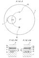
- a polishing apparatus has a turntable 1 constituting a polishing table, and a top ring 3 for holding a semiconductor wafer 2 and pressing the semiconductor wafer 2 against the turntable 1.
- the turntable 1 is coupled to a motor 7, and is rotatable about its own axis, as indicated by the arrow.
- a polishing cloth 4 is mounted on an upper surface of the turntable 1.
- the top ring 3 is coupled to a motor (not shown) and connected to a lifting/lowering cylinder (not shown). Therefore, the top ring 3 is vertically movable and rotatable about its own axis, as indicated by the arrows, and can press the semiconductor wafer 2 against the polishing cloth 4 under a desired pressure.
- the top ring 3 is connected to the lower end of a vertical top ring drive shaft 8, and supports on its lower surface an elastic pad 9 of polyurethane or the like.
- a cylindrical retainer ring 6 is provided around an outer circumferential edge of the top ring 3 for preventing the semiconductor wafer 2 from being dislodged from the top ring 3 while the semiconductor wafer 2 is being polished.
- a polishing liquid supply nozzle 5 is disposed above the turntable 1 for supplying a polishing liquid Q to the polishing cloth 4 on the turntable 1.
- the turntable 1 houses therein an eddy-current sensor 10 which is electrically connected to a controller 12 by a wire 14 extending through the turntable 1, a turntable support shaft la, and a rotary connector or slip ring 11 mounted on a lower end of the turntable support shaft la.
- the controller 12 is connected to a display unit 13.
- FIG. 2 shows the turntable 1 in plan.
- the eddy-current sensor 10 is positioned so as to pass through the center C w of the semiconductor wafer 2 held by the top ring 3 while the semiconductor wafer 2 is being polished, when the turntable 1 rotates about its own axis C T . While the eddy-current sensor 10 passes along an arcuate path beneath the semiconductor wafer 2, the eddy-current sensor 10 continuously detects the thickness of a conductive layer such as a copper layer on the semiconductor wafer 2.
- FIGS. 3A and 3B show the eddy-current sensor 10 which is mounted in the turntable 1.
- FIG. 3A shows the eddy-current sensor 10 mounted in the turntable 1 with the polishing cloth 4 attached thereto
- FIG. 3B shows the eddy-current sensor 10 mounted on the turntable 1 with a fixed abrasive plate 15 attached thereto. If the polishing cloth 4 is mounted on the turntable 1 as shown in FIG. 3A, then the eddy-current sensor 10 is mounted in the turntable 1. If the fixed abrasive plate 15 is mounted on the turntable 1 as shown in FIG. 3B, then the eddy-current sensor 10 is mounted on the turntable 1 and provided in the fixed abrasive plate 15.
- the upper surface i.e. the polishing surface of the polishing cloth 4 or the fixed abrasive plate 15 (the polished surface of the semiconductor wafer 2) may be spaced from the upper surface of the eddy-current sensor 10 by a distance L of 1.3 mm or more.
- the semiconductor wafer 2 comprises an oxide film 2a of SiO 2 , and a conductive layer 2b of copper or aluminum provided on the oxide film 2a.
- the polishing cloth 4 comprises a nonwoven fabric such as Politex manufactured by Rodel Products Corporation, or polyurethane foam such as IC1000.
- the fixed abrasive plate 15 comprises a disk of fine abrasive particles of, for example, CeO 2 having a particle size of several ⁇ m or less and bonded together by a binder of synthetic resin.
- the polishing apparatus shown in FIG. 2 operates as follows: The semiconductor wafer 2 is held on the lower surface of the top ring 3, and pressed by the lifting/lowering cylinder against the polishing cloth 4 on the turntable 1 which is rotating.
- the polishing liquid supply nozzle 5 supplies the polishing liquid Q to the polishing cloth 4 on the turntable 1, and the supplied polishing liquid Q is retained on the polishing cloth 4.
- the semiconductor wafer 2 is polished in the presence of the polishing liquid Q between the lower surface of the semiconductor wafer 2 and the polishing cloth 4. While the semiconductor wafer 2 is being thus polished, the eddy-current sensor 10 passes directly beneath the surface, being polished, of the semiconductor wafer 2 each time the turntable 1 makes one revolution.
- the eddy-current sensor 10 Since the eddy-current sensor 10 is positioned on an arcuate path extending through the center C w of the semiconductor wafer 2, the eddy-current sensor 10 is capable of continuously detecting the thickness of the conductive layer 2b on the semiconductor wafer 2 as the eddy-current sensor 10 moves along the arcuate path beneath the semiconductor wafer 2. In order to shorten the interval between detecting intervals, one or more eddy-current sensors 10 may be added as indicated by the imaginary lines in FIG. 2, so that at least two sensors are provided in the turntable 1.
- the eddy-current sensor has a coil which is supplied with a high-frequency current.
- a high-frequency current is supplied to the coil of the eddy-current sensor, an eddy current is generated in the conductive layer on the semiconductor wafer. Since the generated eddy current varies depending on the thickness of the conductive layer, the combined impedance of the eddy-current sensor and the conductive layer is monitored to detect an end point of the CMP process.
- the combined impedance Z of the eddy-current sensor and the conductive layer is represented by the inductive and capacitive elements L, C of the eddy-current sensor, and the resistive element R of the conductive layer which is connected parallel to the inductive and capacitive elements L, C.
- the combined impedance Z also varies.
- the resonance frequency also varies, and a rate of change of the resonance frequency is monitored to determine an end point of the CMP process.
- Z j ⁇ ⁇ ⁇ L 1 - ⁇ 2 ⁇ LC + j ⁇ ⁇ ⁇ L R
- Z combined impedance
- j square root of -1 (imaginary number)
- L inductance
- f resonance frequency
- C electrostatic capacitance
- R resistance of the conductive layer
- ⁇ 2 ⁇ f.
- FIGS. 4A and 4B are graphs showing changes in the resonance frequency of a detected signal that is produced by the eddy-current sensor 10 and processed by the controller 12 while the semiconductor wafer 2 is being polished.
- the horizontal axis represents polishing time
- the vertical axis represents the resonance frequency (Hz).
- FIG. 4A shows changes in the resonance frequency when the eddy-current sensor 10 passes a plurality of times directly below the semiconductor wafer 2
- FIG. 4B shows, at an enlarged scale, an encircled portion A in FIG. 4A.
- the result shown in FIGS. 4A and 4B is obtained when the conductive layer on the semiconductor wafer 2 is a copper film.
- the value produced by processing the detected signal from the eddy-current sensor 10 is progressively reduced.
- This processing of the detected signal is performed by the controller 12.
- the resonance frequency obtained by processing the detected signal from the eddy-current sensor 10 is progressively reduced.
- the resonance frequency decreases from an initial value of 6800 Hz. Therefore, if the value of the resonance frequency, at the time when the conductive layer is removed except for the conductive layer in the interconnection grooves, has been examined, then an end point of the CMP process can be detected by monitoring the value of the resonance frequency.
- the value of the resonance frequency at the time when the conductive layer is removed except for the conductive layer in the interconnection grooves is 6620 Hz. If a certain frequency before reaching the end point of the CMP process is established as a threshold, then it is possible to polish the semiconductor wafer 2 with the fixed abrasive plate 15 (see FIG. 3B) at a higher polishing rate, then polish the semiconductor wafer 2 with the polishing cloth 4 (see FIG. 3A) at a lower polishing rate after the threshold is reached, and finish the CMP process when the end point thereof is reached.
- the eddy-current sensor has different sensitivity for measuring the thickness of the conductive layer depending on the frequency of the high-frequency current supplied to the sensor coil. For example, when the high-frequency current having a frequency of 20 MHz is supplied to the sensor coil, the eddy-current sensor can measure the thickness of the conductive layer over a wide range of thickness from 0 to 10000 ⁇ , and when the high-frequency current having a frequency of 160 MHz is supplied to the sensor coil, the eddy-current sensor is sensitive to the thickness of the conductive layer in a relatively narrow range of thickness from 0 to 1000 ⁇ .
- the eddy-current sensor may be changed depending on the polishing process.
- a change in the resonance frequency within the polished surface of the semiconductor wafer 2 can be detected. Specifically, since a change in the resonance frequency corresponds to a change in the thickness of the conductive layer and the eddy-current sensor 10 is positioned so as to pass through the center C w of the semiconductor wafer 2, the polishing uniformity of the semiconductor wafer 2 in a substantially diametrical direction thereof can be detected by monitoring the detected signal from the eddy-current sensor 10.
- polishing conditions including the pressing force applied to the top ring 3 to press the semiconductor layer 2 and the distribution of pressures applied to the upper surface of the semiconductor wafer 2 can be changed to improve the polishing uniformity within the polished surface of the semiconductor wafer 2.
- FIG. 5 is a graph showing changes in the resonance frequency of a detected signal that is produced by the eddy-current sensor 10 and processed by the controller 12 while a plurality of semiconductor wafers are being polished by a single polishing cloth.
- the horizontal axis represents polishing time
- the vertical axis represents the resonance frequency (Hz).
- the polishing cloth is worn by a thickness of 0.7 mm after the polishing cloth has polished a plurality of semiconductor wafers and has been dressed a plurality of times.
- the resonance frequency obtained by processing the detected signal from the eddy-current sensor 10 each time a polishing cycle starts is higher when the polishing cloth has been repeatedly used than when the polishing cloth is used for the first time. Specifically, the resonance frequency increases from 6800 Hz when the polishing cloth is used for the first time to 6900 Hz when the polishing cloth has been repeatedly used. Since the rate of abrasion of the polishing cloth can be determined by monitoring the resonance frequency each time a polishing cycle starts, the timing to replace the polishing cloth can accurately be determined.
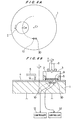
- FIGS. 6A and 6B show a polishing apparatus according to the present invention.
- FIG. 6A is a plan view of a turntable in the polishing apparatus
- FIG. 6B is a vertical cross-sectional view of the polishing apparatus.
- the polishing apparatus shown in FIGS. 6A and 6B is different from the polishing apparatus shown in FIGS. 1 and 2 in that an optical sensor 30 is mounted in the turntable 1 adjacent to the eddy-current sensor 10 and connected to a controller 32.
- the optical sensor 30 comprises a light-emitting element and a light-detecting element.
- the light-emitting element applies light to the surface, being polished, of the semiconductor wafer 2, and the light-detecting element detects reflected light from the surface, being polished, of the semiconductor wafer 2.
- the light-emitting element comprises a laser beam source or an LED.
- the thickness of the conductive layer of copper, aluminum or the like is reduced to a certain smaller value, a portion of the light applied from the light-emitting element to the surface, being polished, of the semiconductor wafer 2 passes through the conductive layer and is reflected from the surface of the oxide film under the conductive layer. Therefore, the light-detecting element detects both the light reflected by the conductive layer and the light reflected by the oxide film. A detected signal from the light-detecting element is processed by the controller 32 to detect the thickness of the conductive layer remaining on the oxide film more accurately than the eddy-current sensor 10.
- the thickness of the conductive layer is monitored by the controller 12 which processes the signal from the eddy-current sensor 10.
- the controller 32 which processes the signal from the optical sensor 30. Therefore, by using the optical sensor 30 which is of a higher sensitivity to the thickness of the conductive layer (film), it is possible to accurately detect the time when the conductive layer is removed except for the conductive layer in the interconnection grooves, thereby determining an end point of the CMP process.
- both the eddy-current sensor 10 and the optical sensor 30 can be used until an end point of the CMP process is reached.
- the controllers 12 and 32 process the respective signals from the eddy-current sensor 10 and the optical sensor 30 to detect the time when the conductive layer is removed except for the conductive layer in the interconnection grooves, thereby determining an end of the CMP process.
- the conductive layer is made of copper or aluminum.
- the conductive layer may be made of chromium, tungsten, titanium, or the like.
- an eddy-current sensor and an optical sensor are mounted in a polishing table which supports a polishing cloth or a fixed abrasive plate thereon, it is possible to obtain a real-time continuous measured value that represents the thickness of a conductive layer made of copper, aluminum, or the like on a surface of a semiconductor substrate which is being polished by the polishing apparatus.
Landscapes
- Engineering & Computer Science (AREA)
- Mechanical Engineering (AREA)
- Mechanical Treatment Of Semiconductor (AREA)
- Finish Polishing, Edge Sharpening, And Grinding By Specific Grinding Devices (AREA)
Claims (5)
- Poliervorrichtung, die Folgendes aufweist:einen drehbaren Poliertisch (1) mit einer Polieroberfläche;einen Oberring (3) zum Halten eines Substrats (2) mit einer Mitte (Cw) und zum Pressen einer Oberfläche des Substrats (2) gegen die Polieroberfläche zum Polieren der Oberfläche des Substrats,mindestens einen Sensor (10) angeordnet unterhalb der erwähnten Polieroberfläche des Poliertischs (1) zur Messung der Dicke einer auf der Oberfläche des Substrats gebildeten leitenden Schicht, und wobei der Sensor einen Wirbelstromsensor (10) aufweist und wobei der Wirbelstromsensor (10) dazu verwendet wird, den Polierprozess zu überwachen und zwar durch Überwachung der kombinierten Impedanz des Wirbelstromsensors (10) und der leitenden Schicht, und wobei ferner mindestens ein optischer Sensor (30) im Poliertisch (1) zum Messen der Dicke der leitenden Schicht angebracht ist.
- Poliervorrichtung nach Anspruch 1, wobei der Wirbelstromsensor (10) im Poliertisch (1) angeordnet ist.
- Poliervorrichtung nach Anspruch 1, wobei die Polieroberfläche ein Poliertuch (4) aufweist.
- Poliervorrichtung nach Anspruch 1, wobei die Polieroberfläche eine befestigte Abriebplatte aufweist.
- Poliervorrichtung nach Anspruch 4, wobei der Wirbelstromsensor (10) in der befestigten Abriebplatte vorgesehen ist.
Applications Claiming Priority (2)
| Application Number | Priority Date | Filing Date | Title |
|---|---|---|---|
| JP2000008393 | 2000-01-17 | ||
| JP2000008393 | 2000-01-17 |
Publications (3)
| Publication Number | Publication Date |
|---|---|
| EP1116552A2 EP1116552A2 (de) | 2001-07-18 |
| EP1116552A3 EP1116552A3 (de) | 2004-01-02 |
| EP1116552B1 true EP1116552B1 (de) | 2007-04-18 |
Family
ID=18536670
Family Applications (1)
| Application Number | Title | Priority Date | Filing Date |
|---|---|---|---|
| EP01100187A Expired - Lifetime EP1116552B1 (de) | 2000-01-17 | 2001-01-17 | Poliermaschine mit Dickemessvorrichtung |
Country Status (5)
| Country | Link |
|---|---|
| US (3) | US6558229B2 (de) |
| EP (1) | EP1116552B1 (de) |
| KR (1) | KR100718737B1 (de) |
| DE (1) | DE60127884T2 (de) |
| TW (1) | TW471993B (de) |
Cited By (1)
| Publication number | Priority date | Publication date | Assignee | Title |
|---|---|---|---|---|
| US8337278B2 (en) | 2007-09-24 | 2012-12-25 | Applied Materials, Inc. | Wafer edge characterization by successive radius measurements |
Families Citing this family (68)
| Publication number | Priority date | Publication date | Assignee | Title |
|---|---|---|---|---|
| KR100718737B1 (ko) * | 2000-01-17 | 2007-05-15 | 가부시키가이샤 에바라 세이사꾸쇼 | 폴리싱 장치 |
| US6924641B1 (en) * | 2000-05-19 | 2005-08-02 | Applied Materials, Inc. | Method and apparatus for monitoring a metal layer during chemical mechanical polishing |
| US8485862B2 (en) * | 2000-05-19 | 2013-07-16 | Applied Materials, Inc. | Polishing pad for endpoint detection and related methods |
| US20020023715A1 (en) * | 2000-05-26 | 2002-02-28 | Norio Kimura | Substrate polishing apparatus and substrate polishing mehod |
| JP3916375B2 (ja) * | 2000-06-02 | 2007-05-16 | 株式会社荏原製作所 | ポリッシング方法および装置 |
| US6878038B2 (en) * | 2000-07-10 | 2005-04-12 | Applied Materials Inc. | Combined eddy current sensing and optical monitoring for chemical mechanical polishing |
| US6602724B2 (en) | 2000-07-27 | 2003-08-05 | Applied Materials, Inc. | Chemical mechanical polishing of a metal layer with polishing rate monitoring |
| TW541425B (en) * | 2000-10-20 | 2003-07-11 | Ebara Corp | Frequency measuring device, polishing device using the same and eddy current sensor |
| US6608495B2 (en) | 2001-03-19 | 2003-08-19 | Applied Materials, Inc. | Eddy-optic sensor for object inspection |
| US6966816B2 (en) | 2001-05-02 | 2005-11-22 | Applied Materials, Inc. | Integrated endpoint detection system with optical and eddy current monitoring |
| JP4131632B2 (ja) * | 2001-06-15 | 2008-08-13 | 株式会社荏原製作所 | ポリッシング装置及び研磨パッド |
| US6811466B1 (en) * | 2001-12-28 | 2004-11-02 | Applied Materials, Inc. | System and method for in-line metal profile measurement |
| US7001242B2 (en) | 2002-02-06 | 2006-02-21 | Applied Materials, Inc. | Method and apparatus of eddy current monitoring for chemical mechanical polishing |
| JP2005517290A (ja) * | 2002-02-06 | 2005-06-09 | アプライド マテリアルズ インコーポレイテッド | 渦電流モニタリングシステムを備えた化学機械的研磨の為の方法及び装置 |
| US7131889B1 (en) * | 2002-03-04 | 2006-11-07 | Micron Technology, Inc. | Method for planarizing microelectronic workpieces |
| ITFI20020077A1 (it) | 2002-05-10 | 2003-11-10 | Galileo Vacuum Systems S R L | Dispositivo per la determinazione dello spessore di uno strato conduttivo |
| US6929531B2 (en) * | 2002-09-19 | 2005-08-16 | Lam Research Corporation | System and method for metal residue detection and mapping within a multi-step sequence |
| IL153894A (en) | 2003-01-12 | 2010-05-31 | Nova Measuring Instr Ltd | Method and system for measuring the thickness of thin conductive layers |
| US7016795B2 (en) * | 2003-02-04 | 2006-03-21 | Applied Materials Inc. | Signal improvement in eddy current sensing |
| US6945845B2 (en) * | 2003-03-04 | 2005-09-20 | Applied Materials, Inc. | Chemical mechanical polishing apparatus with non-conductive elements |
| US7008296B2 (en) * | 2003-06-18 | 2006-03-07 | Applied Materials, Inc. | Data processing for monitoring chemical mechanical polishing |
| JP2005015885A (ja) * | 2003-06-27 | 2005-01-20 | Ebara Corp | 基板処理方法及び装置 |
| US7470288B2 (en) * | 2003-07-11 | 2008-12-30 | Depuy Products, Inc. | Telemetric tibial tray |
| WO2005007025A2 (en) * | 2003-07-11 | 2005-01-27 | Depuy Products, Inc. | In vivo joint implant cycle counter |
| JP4777243B2 (ja) * | 2003-07-11 | 2011-09-21 | デピュイ・プロダクツ・インコーポレイテッド | 体内での関節空間測定装置および測定方法 |
| US7218232B2 (en) * | 2003-07-11 | 2007-05-15 | Depuy Products, Inc. | Orthopaedic components with data storage element |
| US7112960B2 (en) | 2003-07-31 | 2006-09-26 | Applied Materials, Inc. | Eddy current system for in-situ profile measurement |
| US7025658B2 (en) * | 2003-08-18 | 2006-04-11 | Applied Materials, Inc. | Platen and head rotation rates for monitoring chemical mechanical polishing |
| US7153185B1 (en) | 2003-08-18 | 2006-12-26 | Applied Materials, Inc. | Substrate edge detection |
| US7299151B2 (en) * | 2004-02-04 | 2007-11-20 | Hewlett-Packard Development Company, L.P. | Microdevice processing systems and methods |
| US20050211667A1 (en) * | 2004-03-26 | 2005-09-29 | Lam Research Corporation | Method and apparatus for measurement of thin films and residues on semiconductor substrates |
| US7052364B2 (en) * | 2004-06-14 | 2006-05-30 | Cabot Microelectronics Corporation | Real time polishing process monitoring |
| EP1758711B1 (de) * | 2004-06-21 | 2013-08-07 | Ebara Corporation | Poliervorrichtung und polierverfahren |
| TWI275451B (en) * | 2005-01-11 | 2007-03-11 | Asia Ic Mic Process Inc | Measurement of thickness profile and elastic modulus profile of polishing pad |
| US20060226123A1 (en) * | 2005-04-07 | 2006-10-12 | Applied Materials, Inc. | Profile control using selective heating |
| JP2009129970A (ja) * | 2007-11-20 | 2009-06-11 | Ebara Corp | 研磨装置及び研磨方法 |
| TWI450792B (zh) * | 2008-08-05 | 2014-09-01 | Ebara Corp | 研磨方法及裝置 |
| US20100041316A1 (en) * | 2008-08-14 | 2010-02-18 | Yulin Wang | Method for an improved chemical mechanical polishing system |
| JP5611214B2 (ja) | 2008-10-16 | 2014-10-22 | アプライド マテリアルズ インコーポレイテッドApplied Materials,Incorporated | 渦電流利得の補償 |
| JP5615831B2 (ja) | 2008-11-14 | 2014-10-29 | アプライド マテリアルズ インコーポレイテッドApplied Materials,Incorporated | 縁部分解能強化渦電流センサ |
| US20110124269A1 (en) * | 2009-07-16 | 2011-05-26 | Mitsuo Tada | Eddy current sensor and polishing method and apparatus |
| JP5407693B2 (ja) * | 2009-09-17 | 2014-02-05 | 旭硝子株式会社 | ガラス基板の製造方法、研磨方法及び研磨装置、並びにガラス基板 |
| KR101526039B1 (ko) * | 2009-09-22 | 2015-06-04 | 아뎀, 엘엘씨 | 공진형 임피던스 센서, 임피던스 감지 시스템 및 물체의 화학적 및 물리적 특성을 측정하는 방법 |
| US8377825B2 (en) * | 2009-10-30 | 2013-02-19 | Corning Incorporated | Semiconductor wafer re-use using chemical mechanical polishing |
| US20110189856A1 (en) * | 2010-01-29 | 2011-08-04 | Kun Xu | High Sensitivity Real Time Profile Control Eddy Current Monitoring System |
| JP5980476B2 (ja) * | 2010-12-27 | 2016-08-31 | 株式会社荏原製作所 | ポリッシング装置およびポリッシング方法 |
| US20120276817A1 (en) * | 2011-04-27 | 2012-11-01 | Iravani Hassan G | Eddy current monitoring of metal residue or metal pillars |
| US9528814B2 (en) | 2011-05-19 | 2016-12-27 | NeoVision, LLC | Apparatus and method of using impedance resonance sensor for thickness measurement |
| US9418904B2 (en) | 2011-11-14 | 2016-08-16 | Taiwan Semiconductor Manufacturing Co., Ltd. | Localized CMP to improve wafer planarization |
| US9465089B2 (en) | 2011-12-01 | 2016-10-11 | Neovision Llc | NMR spectroscopy device based on resonance type impedance (IR) sensor and method of NMR spectra acquisition |
| US8952708B2 (en) | 2011-12-02 | 2015-02-10 | Neovision Llc | Impedance resonance sensor for real time monitoring of different processes and methods of using same |
| US10065288B2 (en) | 2012-02-14 | 2018-09-04 | Taiwan Semiconductor Manufacturing Co., Ltd. | Chemical mechanical polishing (CMP) platform for local profile control |
| JP6033751B2 (ja) * | 2013-10-07 | 2016-11-30 | 株式会社荏原製作所 | 研磨方法 |
| US9676075B2 (en) | 2015-06-12 | 2017-06-13 | Globalfoundries Inc. | Methods and structures for achieving target resistance post CMP using in-situ resistance measurements |
| WO2018080764A1 (en) | 2016-10-28 | 2018-05-03 | Applied Materials, Inc. | Core configuration with alternating posts for in-situ electromagnetic induction monitoring system |
| TWI816620B (zh) | 2017-04-21 | 2023-09-21 | 美商應用材料股份有限公司 | 使用神經網路來監測的拋光裝置 |
| US10898986B2 (en) | 2017-09-15 | 2021-01-26 | Applied Materials, Inc. | Chattering correction for accurate sensor position determination on wafer |
| EP3691830A4 (de) * | 2017-10-04 | 2021-11-17 | Saint-Gobain Abrasives, Inc. | Schleifartikel und verfahren zur herstellung davon |
| TWI845444B (zh) | 2018-04-03 | 2024-06-11 | 美商應用材料股份有限公司 | 針對墊子厚度使用機器學習及補償的拋光裝置、拋光系統、方法及電腦儲存媒體 |
| TWI828706B (zh) | 2018-06-20 | 2024-01-11 | 美商應用材料股份有限公司 | 用於原位電磁感應監控的基板摻雜補償的方法、電腦程式產品及研磨系統 |
| CN111886686B (zh) | 2018-09-26 | 2024-08-02 | 应用材料公司 | 针对原位电磁感应监测的边缘重建中的基板掺杂的补偿 |
| EP3948702A4 (de) | 2019-03-29 | 2023-07-26 | Saint-Gobain Abrasives, Inc. | Lösungen für leistungsschleifen |
| WO2020206382A1 (en) | 2019-04-03 | 2020-10-08 | Saint-Gobain Abrasives, Inc. | Abrasive article, abrasive system and method for using and forming same |
| WO2021231427A1 (en) | 2020-05-14 | 2021-11-18 | Applied Materials, Inc. | Technique for training neural network for use in in-situ monitoring during polishing and polishing system |
| KR102732531B1 (ko) | 2020-06-24 | 2024-11-21 | 어플라이드 머티어리얼스, 인코포레이티드 | 연마 패드 마모 보상을 이용한 기판 층 두께의 결정 |
| WO2022010687A1 (en) * | 2020-07-08 | 2022-01-13 | Applied Materials, Inc. | Multi-toothed, magnetically controlled retaining ring |
| US11794302B2 (en) | 2020-12-15 | 2023-10-24 | Applied Materials, Inc. | Compensation for slurry composition in in-situ electromagnetic inductive monitoring |
| CN115741448A (zh) * | 2022-12-15 | 2023-03-07 | 安徽富乐德长江半导体材料股份有限公司 | 一种晶圆研磨厚度控制装置及系统 |
Family Cites Families (30)
| Publication number | Priority date | Publication date | Assignee | Title |
|---|---|---|---|---|
| US4793895A (en) * | 1988-01-25 | 1988-12-27 | Ibm Corporation | In situ conductivity monitoring technique for chemical/mechanical planarization endpoint detection |
| US5081421A (en) * | 1990-05-01 | 1992-01-14 | At&T Bell Laboratories | In situ monitoring technique and apparatus for chemical/mechanical planarization endpoint detection |
| US5213655A (en) * | 1990-05-16 | 1993-05-25 | International Business Machines Corporation | Device and method for detecting an end point in polishing operation |
| US5240552A (en) * | 1991-12-11 | 1993-08-31 | Micron Technology, Inc. | Chemical mechanical planarization (CMP) of a semiconductor wafer using acoustical waves for in-situ end point detection |
| US5265378A (en) * | 1992-07-10 | 1993-11-30 | Lsi Logic Corporation | Detecting the endpoint of chem-mech polishing and resulting semiconductor device |
| US6614529B1 (en) * | 1992-12-28 | 2003-09-02 | Applied Materials, Inc. | In-situ real-time monitoring technique and apparatus for endpoint detection of thin films during chemical/mechanical polishing planarization |
| US5433651A (en) * | 1993-12-22 | 1995-07-18 | International Business Machines Corporation | In-situ endpoint detection and process monitoring method and apparatus for chemical-mechanical polishing |
| JP3313505B2 (ja) * | 1994-04-14 | 2002-08-12 | 株式会社日立製作所 | 研磨加工法 |
| US5893796A (en) * | 1995-03-28 | 1999-04-13 | Applied Materials, Inc. | Forming a transparent window in a polishing pad for a chemical mechanical polishing apparatus |
| US5964643A (en) * | 1995-03-28 | 1999-10-12 | Applied Materials, Inc. | Apparatus and method for in-situ monitoring of chemical mechanical polishing operations |
| US5838447A (en) * | 1995-07-20 | 1998-11-17 | Ebara Corporation | Polishing apparatus including thickness or flatness detector |
| JPH1034529A (ja) * | 1996-07-18 | 1998-02-10 | Speedfam Co Ltd | 自動定寸装置 |
| US6146248A (en) * | 1997-05-28 | 2000-11-14 | Lam Research Corporation | Method and apparatus for in-situ end-point detection and optimization of a chemical-mechanical polishing process using a linear polisher |
| JPH11114813A (ja) * | 1997-10-07 | 1999-04-27 | Speedfam Co Ltd | 研磨システム及びその制御方法 |
| US6068539A (en) * | 1998-03-10 | 2000-05-30 | Lam Research Corporation | Wafer polishing device with movable window |
| US6248000B1 (en) * | 1998-03-24 | 2001-06-19 | Nikon Research Corporation Of America | Polishing pad thinning to optically access a semiconductor wafer surface |
| US6132289A (en) * | 1998-03-31 | 2000-10-17 | Lam Research Corporation | Apparatus and method for film thickness measurement integrated into a wafer load/unload unit |
| US5897426A (en) * | 1998-04-24 | 1999-04-27 | Applied Materials, Inc. | Chemical mechanical polishing with multiple polishing pads |
| JPH11325840A (ja) * | 1998-05-19 | 1999-11-26 | Dainippon Screen Mfg Co Ltd | メタル残膜判定方法およびメタル残膜判定装置 |
| US6159073A (en) | 1998-11-02 | 2000-12-12 | Applied Materials, Inc. | Method and apparatus for measuring substrate layer thickness during chemical mechanical polishing |
| US6204922B1 (en) * | 1998-12-11 | 2001-03-20 | Filmetrics, Inc. | Rapid and accurate thin film measurement of individual layers in a multi-layered or patterned sample |
| US6172756B1 (en) * | 1998-12-11 | 2001-01-09 | Filmetrics, Inc. | Rapid and accurate end point detection in a noisy environment |
| US6247998B1 (en) * | 1999-01-25 | 2001-06-19 | Applied Materials, Inc. | Method and apparatus for determining substrate layer thickness during chemical mechanical polishing |
| US6190234B1 (en) * | 1999-01-25 | 2001-02-20 | Applied Materials, Inc. | Endpoint detection with light beams of different wavelengths |
| US6213845B1 (en) * | 1999-04-26 | 2001-04-10 | Micron Technology, Inc. | Apparatus for in-situ optical endpointing on web-format planarizing machines in mechanical or chemical-mechanical planarization of microelectronic-device substrate assemblies and methods for making and using same |
| US6234870B1 (en) * | 1999-08-24 | 2001-05-22 | International Business Machines Corporation | Serial intelligent electro-chemical-mechanical wafer processor |
| US6433541B1 (en) | 1999-12-23 | 2002-08-13 | Kla-Tencor Corporation | In-situ metalization monitoring using eddy current measurements during the process for removing the film |
| EP1244907A1 (de) | 1999-12-23 | 2002-10-02 | KLA-Tencor Corporation | Vor-ort-überwachung für metallisationsprozesse unter verwendung von wirbelstrommessungen und optischen messungen |
| KR100718737B1 (ko) * | 2000-01-17 | 2007-05-15 | 가부시키가이샤 에바라 세이사꾸쇼 | 폴리싱 장치 |
| US7001242B2 (en) * | 2002-02-06 | 2006-02-21 | Applied Materials, Inc. | Method and apparatus of eddy current monitoring for chemical mechanical polishing |
-
2001
- 2001-01-16 KR KR1020010002419A patent/KR100718737B1/ko not_active Expired - Lifetime
- 2001-01-17 EP EP01100187A patent/EP1116552B1/de not_active Expired - Lifetime
- 2001-01-17 TW TW090100998A patent/TW471993B/zh not_active IP Right Cessation
- 2001-01-17 DE DE60127884T patent/DE60127884T2/de not_active Expired - Fee Related
- 2001-01-17 US US09/760,823 patent/US6558229B2/en not_active Expired - Lifetime
-
2003
- 2003-03-17 US US10/388,508 patent/US6764381B2/en not_active Expired - Lifetime
-
2004
- 2004-06-10 US US10/864,322 patent/US6984164B2/en not_active Expired - Lifetime
Cited By (1)
| Publication number | Priority date | Publication date | Assignee | Title |
|---|---|---|---|---|
| US8337278B2 (en) | 2007-09-24 | 2012-12-25 | Applied Materials, Inc. | Wafer edge characterization by successive radius measurements |
Also Published As
| Publication number | Publication date |
|---|---|
| US6764381B2 (en) | 2004-07-20 |
| EP1116552A2 (de) | 2001-07-18 |
| KR100718737B1 (ko) | 2007-05-15 |
| KR20010076286A (ko) | 2001-08-11 |
| US6984164B2 (en) | 2006-01-10 |
| DE60127884T2 (de) | 2008-01-17 |
| EP1116552A3 (de) | 2004-01-02 |
| DE60127884D1 (de) | 2007-05-31 |
| US20010008827A1 (en) | 2001-07-19 |
| TW471993B (en) | 2002-01-11 |
| US20030171071A1 (en) | 2003-09-11 |
| US6558229B2 (en) | 2003-05-06 |
| US20040224613A1 (en) | 2004-11-11 |
Similar Documents
| Publication | Publication Date | Title |
|---|---|---|
| EP1116552B1 (de) | Poliermaschine mit Dickemessvorrichtung | |
| US6663469B2 (en) | Polishing method and apparatus | |
| EP0455455B1 (de) | In-Situ-Kontrolltechnik und Gerät zum Bestimmen des Endes eines chemisch-mechanischen Planiervorganges | |
| US6319420B1 (en) | Method and apparatus for electrically endpointing a chemical-mechanical planarization process | |
| US5705435A (en) | Chemical-mechanical polishing (CMP) apparatus | |
| EP0325753B1 (de) | System zum Kontrollieren der Leitfähigkeit eines Halbleiterplättchens während des Schleifens | |
| US7314401B2 (en) | Methods and systems for conditioning planarizing pads used in planarizing substrates | |
| US6515493B1 (en) | Method and apparatus for in-situ endpoint detection using electrical sensors | |
| US20050173259A1 (en) | Endpoint system for electro-chemical mechanical polishing | |
| CN113231955B (zh) | 一种涡电流传感器的测厚校准方法、装置及研磨系统 | |
| US20050118839A1 (en) | Chemical mechanical polish process control method using thermal imaging of polishing pad | |
| KR20050057506A (ko) | 멀티-스텝 시퀀스에서의 금속 잔류물 검출 및 매핑용시스템 및 방법 | |
| EP0987744B1 (de) | Verfahren zur Optimierung von Metall-CMP-Prozessen | |
| KR102944366B1 (ko) | 연마에서 진동을 검출하기 위한 와전류 모니터링 | |
| JP3907414B2 (ja) | ポリッシング装置 | |
| KR102598487B1 (ko) | 웨이퍼 상의 정확한 센서 위치 결정을 위한 채터링 보정 | |
| JP2001198813A (ja) | 研磨装置及びその研磨方法 | |
| KR20250018544A (ko) | 음향 신호들을 이용한 기판 배향 결정 | |
| JPH10202508A (ja) | 研磨方法 | |
| US20250062163A1 (en) | Acoustic monitoring for process reliability during polishing | |
| JPH10144634A (ja) | 化学/機械的ポリシング装置及び方法 | |
| KR19990025212A (ko) | 웨이퍼 연마 방법 |
Legal Events
| Date | Code | Title | Description |
|---|---|---|---|
| PUAI | Public reference made under article 153(3) epc to a published international application that has entered the european phase |
Free format text: ORIGINAL CODE: 0009012 |
|
| AK | Designated contracting states |
Kind code of ref document: A2 Designated state(s): AT BE CH CY DE DK ES FI FR GB GR IE IT LI LU MC NL PT SE TR |
|
| AX | Request for extension of the european patent |
Free format text: AL;LT;LV;MK;RO;SI |
|
| PUAL | Search report despatched |
Free format text: ORIGINAL CODE: 0009013 |
|
| RIC1 | Information provided on ipc code assigned before grant |
Ipc: 7B 24B 49/10 B Ipc: 7H 01L 21/306 - Ipc: 7B 24B 37/04 A Ipc: 7B 24B 7/22 B Ipc: 7B 24B 49/04 B |
|
| AK | Designated contracting states |
Kind code of ref document: A3 Designated state(s): AT BE CH CY DE DK ES FI FR GB GR IE IT LI LU MC NL PT SE TR |
|
| AX | Request for extension of the european patent |
Extension state: AL LT LV MK RO SI |
|
| 17P | Request for examination filed |
Effective date: 20040628 |
|
| AKX | Designation fees paid |
Designated state(s): DE FR |
|
| 17Q | First examination report despatched |
Effective date: 20041119 |
|
| GRAP | Despatch of communication of intention to grant a patent |
Free format text: ORIGINAL CODE: EPIDOSNIGR1 |
|
| GRAS | Grant fee paid |
Free format text: ORIGINAL CODE: EPIDOSNIGR3 |
|
| GRAA | (expected) grant |
Free format text: ORIGINAL CODE: 0009210 |
|
| AK | Designated contracting states |
Kind code of ref document: B1 Designated state(s): DE FR |
|
| REF | Corresponds to: |
Ref document number: 60127884 Country of ref document: DE Date of ref document: 20070531 Kind code of ref document: P |
|
| ET | Fr: translation filed | ||
| PLBE | No opposition filed within time limit |
Free format text: ORIGINAL CODE: 0009261 |
|
| STAA | Information on the status of an ep patent application or granted ep patent |
Free format text: STATUS: NO OPPOSITION FILED WITHIN TIME LIMIT |
|
| 26N | No opposition filed |
Effective date: 20080121 |
|
| PGFP | Annual fee paid to national office [announced via postgrant information from national office to epo] |
Ref country code: DE Payment date: 20090115 Year of fee payment: 9 |
|
| PGFP | Annual fee paid to national office [announced via postgrant information from national office to epo] |
Ref country code: FR Payment date: 20090113 Year of fee payment: 9 |
|
| REG | Reference to a national code |
Ref country code: FR Ref legal event code: ST Effective date: 20100930 |
|
| PG25 | Lapsed in a contracting state [announced via postgrant information from national office to epo] |
Ref country code: FR Free format text: LAPSE BECAUSE OF NON-PAYMENT OF DUE FEES Effective date: 20100201 |
|
| PG25 | Lapsed in a contracting state [announced via postgrant information from national office to epo] |
Ref country code: DE Free format text: LAPSE BECAUSE OF NON-PAYMENT OF DUE FEES Effective date: 20100803 |