EP1114471B1 - Elektrisch stabilisierter dünnschicht-hochtemperatursupraleiter sowie verfahren zur herstellung eines solchen supraleiters - Google Patents
Elektrisch stabilisierter dünnschicht-hochtemperatursupraleiter sowie verfahren zur herstellung eines solchen supraleiters Download PDFInfo
- Publication number
- EP1114471B1 EP1114471B1 EP99932598A EP99932598A EP1114471B1 EP 1114471 B1 EP1114471 B1 EP 1114471B1 EP 99932598 A EP99932598 A EP 99932598A EP 99932598 A EP99932598 A EP 99932598A EP 1114471 B1 EP1114471 B1 EP 1114471B1
- Authority
- EP
- European Patent Office
- Prior art keywords
- layer
- substrate
- area
- openings
- superconductive
- Prior art date
- Legal status (The legal status is an assumption and is not a legal conclusion. Google has not performed a legal analysis and makes no representation as to the accuracy of the status listed.)
- Expired - Lifetime
Links
Images


Classifications
-
- H—ELECTRICITY
- H10—SEMICONDUCTOR DEVICES; ELECTRIC SOLID-STATE DEVICES NOT OTHERWISE PROVIDED FOR
- H10N—ELECTRIC SOLID-STATE DEVICES NOT OTHERWISE PROVIDED FOR
- H10N60/00—Superconducting devices
- H10N60/20—Permanent superconducting devices
- H10N60/203—Permanent superconducting devices comprising high-Tc ceramic materials
-
- H—ELECTRICITY
- H10—SEMICONDUCTOR DEVICES; ELECTRIC SOLID-STATE DEVICES NOT OTHERWISE PROVIDED FOR
- H10N—ELECTRIC SOLID-STATE DEVICES NOT OTHERWISE PROVIDED FOR
- H10N60/00—Superconducting devices
- H10N60/01—Manufacture or treatment
- H10N60/0268—Manufacture or treatment of devices comprising copper oxide
- H10N60/0661—Processes performed after copper oxide formation, e.g. patterning
-
- H—ELECTRICITY
- H10—SEMICONDUCTOR DEVICES; ELECTRIC SOLID-STATE DEVICES NOT OTHERWISE PROVIDED FOR
- H10N—ELECTRIC SOLID-STATE DEVICES NOT OTHERWISE PROVIDED FOR
- H10N60/00—Superconducting devices
- H10N60/30—Devices switchable between superconducting and normal states
Definitions
- the present invention relates to the field of technical application of high temperature superconductors (HTS). It concerns an electrically stabilized Thin-film high-temperature superconductor, comprising a superconducting Layer which is applied to a flat metallic substrate.
- HTS high temperature superconductors
- thin layer HTS is known from the article by K. Hasegawa et al., In-plane Aligned YBCO Thin Film Tape Fabricated by Pulsed Laser Deposition, International Symposium on Superconductivity (ISS '96), Sapporo, Oct. 21-24 (1996), p. 745-748, known.
- HTS high temperature superconductors
- FCL fault Current Limiter
- the bypass is intended to homogenize the distribution of stress by acting as an alternative High current path works when the HTS quivers. In this way, the Formation of "hot spots" are avoided.
- the minimum requirements for one such bypass (1) is a good electrical contact to the HTS and (2) a sufficient thermal capacity to limit the temperature rise.
- a method has been described, such as a high quality thin layer of large length Y-123 (YBCO) a typical metallic substrate (e.g., Hastelloy) by PLD (pulsed laser Deposition) can be applied.
- a separation layer from e.g. Yttrium-stabilized zirconia (YSZ) between the substrate and the HTS provided to the oxidation of the substrate and to prevent the chemical reaction between both layers. It exists therefore no electrical contact between the HTS and the underlying Substrate, which would generally be well suited as an electrical bypass.
- a HTS of the type mentioned characterized in that the superconducting layer is distributed over the surface of the substrate by means of a planar conductive layer applied on the side of the superconducting layer facing away from the substrate Substrate is in electrical contact. Through the distributed over the surface contact between HTS layer and underlying metallic substrate over the area distributed many bypass routes created for the stream, at any time prevent the formation of "hot spots" anywhere on the element can.
- a first preferred embodiment is characterized from that in the superconducting layer and in the underlying Separating layer distributed over the surface contacting openings are arranged, which expose the underlying substrate, that the conductive layer in the region of the contacting openings is guided in contact with the exposed substrate, and that the contacting openings by removing the superconducting layer or the Separation layer are generated.
- the number and distribution of the contact openings can be optimized by conventional masked etching methods that "hot spots" are reliably prevented by the bypassing substrate without that available for the current transport cross-section is unnecessarily reduced.
- a second preferred embodiment is characterized that the contacting openings by covering or shadowing the Application of the superconducting layer or the separating layer are generated. In this Case may involve additional masking and etching steps in the generation the contact openings are dispensed with.
- a first preferred embodiment of the process according to the invention assumes that in a first Step on the metallic substrate over the entire surface of an electrically insulating separation layer is applied in a second step to the electrically insulating Separating layer over the entire surface of the superconducting layer is applied, that in a third step, preferably by a masked etching process, at various Make the surface contact holes in the two applied Layers are generated, through which contacting openings the substrate of freely accessible above, and that in a fourth step over the entire surface of a conductive layer is applied, which contacts the superconducting layer surface and connects through the contacting openings with the exposed substrate.
- a second embodiment of the inventive method is characterized in that a metallic substrate, which is arranged with distributed over the surface pits is provided, in a first step by a directed application of a first Flat surface an electrically insulating separation layer on the substrate is applied, wherein the first direction is chosen so that by shading the bottoms of the pits remain partially uncovered and form contact openings, that in a second step by a directed application from the first Toward the electrically insulating separation layer, the superconducting layer is applied is, and that applied in a third step over the entire surface of a conductive layer which contacts the superconducting layer surface and through the Contact openings on the bottoms of the pits with the exposed substrate combines.
- FIG. 3 The preferred embodiment of FIG. 3 is based on a metallic substrate 31, on the surface of which a separation layer 33 (eg of YSZ or CeO or Y 2 O 3 ) and the actual superconducting layer 32 (eg of YBCO) with the known, in The methods described in the publications mentioned are applied (FIG. 3A).
- a mask layer 34 made of a suitable photoresist or the like is subsequently applied to this layer sequence (FIG. 3B) and subsequently structured by opening mask openings 35 in the mask layer 34 uniformly distributed over the surface (FIG. 3C).
- the outside of the contacting openings 36, the superconducting layer 32nd contacted over the entire surface, and within the contact openings 37 electrically conductive connects with the substrate 31 It goes without saying that the size the contact openings 36 must be chosen so that a sufficient Contacting the substrate 31 is possible. On the other hand, the number and Distribution of the contacting holes 36 are chosen so that for each area the superconducting layer 32 has a sufficient bypass function by the selectively contacted substrate 31 is ensured.
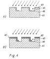
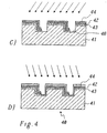
- a selectively contacted substrate is also in the embodiment according to Fig. 4 used.
- a metallic substrate 41 in which on the surface to be coated evenly distributed depressions in Form of pits 45 arranged with preferably vertical side walls are ( Figure 4A).
- an electrically insulating separating layer 43 is applied flatly. The first direction is chosen so that shading by the side walls the bottoms of the pits 45 remain partially uncovered and contact openings 46 form ( Figure 4A).
- a directed application is made from the First direction of the electrically insulating separation layer 43 is a superconducting Layer 42 applied.
- a conductive layer 44 is applied over the entire surface, which is the superconducting Layer 42 contacted flat and through the contact openings 46 on the floors the pits 45 electrically connected to the substrate 41 exposed there.
- a first conductive layer 44 ' which covers the superconducting layer 42 and the contact holes 46 substantially free ( Figure 4C).
- the contacting openings 36, 46 or the pits 45 are preferably formed in the form of trenches parallel to the direction of current flow. In According to the arrangements according to FIG. 3 and FIG. 4, the current therefore flows perpendicularly to shown sectional plane through the high-temperature superconductor.
- the invention results in an electrically stabilized thin-film high-temperature superconductor, for electrical stabilization on the metallic Substrate and the selection of different materials for the substrate allows.
Landscapes
- Engineering & Computer Science (AREA)
- Chemical & Material Sciences (AREA)
- Ceramic Engineering (AREA)
- Manufacturing & Machinery (AREA)
- Superconductor Devices And Manufacturing Methods Thereof (AREA)
- Superconductors And Manufacturing Methods Therefor (AREA)
Applications Claiming Priority (3)
| Application Number | Priority Date | Filing Date | Title |
|---|---|---|---|
| DE19836860 | 1998-08-14 | ||
| DE19836860A DE19836860A1 (de) | 1998-08-14 | 1998-08-14 | Elektrisch stabilisierter Dünnschicht-Hochtemperatursupraleiter sowie Verfahren zur Herstellung eines solchen Verfahrens |
| PCT/CH1999/000359 WO2000010208A1 (de) | 1998-08-14 | 1999-08-02 | Elektrisch stabilisierter dünnschicht-hochtemperatursupraleiter sowie verfahren zur herstellung eines solchen supraleiters |
Publications (2)
| Publication Number | Publication Date |
|---|---|
| EP1114471A1 EP1114471A1 (de) | 2001-07-11 |
| EP1114471B1 true EP1114471B1 (de) | 2005-05-04 |
Family
ID=7877522
Family Applications (1)
| Application Number | Title | Priority Date | Filing Date |
|---|---|---|---|
| EP99932598A Expired - Lifetime EP1114471B1 (de) | 1998-08-14 | 1999-08-02 | Elektrisch stabilisierter dünnschicht-hochtemperatursupraleiter sowie verfahren zur herstellung eines solchen supraleiters |
Country Status (7)
| Country | Link |
|---|---|
| US (1) | US6552415B1 (enExample) |
| EP (1) | EP1114471B1 (enExample) |
| JP (1) | JP4917205B2 (enExample) |
| AU (1) | AU4893899A (enExample) |
| DE (2) | DE19836860A1 (enExample) |
| DK (1) | DK1114471T3 (enExample) |
| WO (1) | WO2000010208A1 (enExample) |
Cited By (1)
| Publication number | Priority date | Publication date | Assignee | Title |
|---|---|---|---|---|
| EP2991126A1 (de) | 2014-08-25 | 2016-03-02 | Theva Dünnschichttechnik GmbH | Verfahren und Vorrichtung zum Herstellen eines Hochtemperatur-Supraleiters |
Families Citing this family (18)
| Publication number | Priority date | Publication date | Assignee | Title |
|---|---|---|---|---|
| DE19957981A1 (de) * | 1999-12-02 | 2001-06-07 | Abb Research Ltd | Hochtemperatursupraleiteranordnung und Verfahren zu deren Herstellung |
| DE10225935C5 (de) * | 2002-06-11 | 2011-10-06 | THEVA DüNNSCHICHTTECHNIK GMBH | Vorrichtung zum Leiten von Strom |
| DE10226391A1 (de) * | 2002-06-13 | 2004-01-08 | Siemens Ag | Resistiver Strombegrenzer wenigstens einer supraleitenden Leiterbahn |
| EP1383178B1 (en) * | 2002-07-15 | 2006-11-02 | Abb Research Ltd. | Superconducting fault current limiter |
| US7496390B2 (en) * | 2004-08-20 | 2009-02-24 | American Superconductor Corporation | Low ac loss filamentary coated superconductors |
| US7463915B2 (en) * | 2004-08-20 | 2008-12-09 | American Superconductor Corporation | Stacked filamentary coated superconductors |
| US7582328B2 (en) * | 2004-08-20 | 2009-09-01 | American Superconductor Corporation | Dropwise deposition of a patterned oxide superconductor |
| DE102004048648B4 (de) * | 2004-10-04 | 2006-08-10 | Siemens Ag | Vorrichtung zur Strombegrenzung vom resistiven Typ mit bandfömigem Hoch-Tc-Supraleiter |
| DE102004048647B4 (de) * | 2004-10-04 | 2006-08-10 | Siemens Ag | Resistive Strombegrenzereinrichtung mit bandförmiger Hoch-Tc-Supraleiterbahn |
| DE102004048646B4 (de) | 2004-10-04 | 2006-08-10 | Siemens Ag | Supraleitende Strombegrenzereinrichtung vom resistiven Typ mit bandförmiger Hoch-Tc-Supraleiterbahn |
| DE102004048644B4 (de) * | 2004-10-04 | 2006-08-10 | Siemens Ag | Vorrichtung zur resistiven Strombegrenzung mit bandförmiger Hoch-Tc -Supraleiterbahn |
| EP1830419B1 (de) | 2006-03-02 | 2009-07-01 | Theva Dünnschichttechnik GmbH | Resistiver Strombegrenzer |
| DE102006032702B3 (de) | 2006-07-14 | 2007-10-04 | Siemens Ag | Resistive supraleitende Strombegrenzeinrichtung mit bifilarer Spulenwicklung aus HTS-Bandleitern und Windungsabstandshalter |
| US7627356B2 (en) * | 2006-07-14 | 2009-12-01 | Superpower, Inc. | Multifilament AC tolerant conductor with striated stabilizer and devices incorporating the same |
| EP2284918A1 (en) * | 2009-08-13 | 2011-02-16 | Nexans | High temperature superconductor, in particular improved coated conductor |
| JP5597516B2 (ja) * | 2010-10-22 | 2014-10-01 | 株式会社フジクラ | 超電導線材の製造方法 |
| US9029296B2 (en) * | 2012-02-02 | 2015-05-12 | Polyvalor, Limited Partnership | Increased normal zone propagation velocity in superconducting segments |
| DE102016217671A1 (de) | 2016-09-15 | 2018-03-15 | Siemens Aktiengesellschaft | Supraleitender Strombegrenzer |
Family Cites Families (20)
| Publication number | Priority date | Publication date | Assignee | Title |
|---|---|---|---|---|
| JPS6474770A (en) * | 1987-09-17 | 1989-03-20 | Fujitsu Ltd | Structure of contact between superconductive film and normal conductive film |
| AU610260B2 (en) | 1987-10-16 | 1991-05-16 | Furukawa Electric Co. Ltd., The | Oxide superconductor shaped body and method of manufacturing the same |
| JPH01171249A (ja) * | 1987-12-25 | 1989-07-06 | Matsushita Electric Ind Co Ltd | 半導体装置の製造方法 |
| JPH01186657A (ja) * | 1988-01-14 | 1989-07-26 | Matsushita Electric Ind Co Ltd | 半導体装置の製造方法 |
| EP0339801B1 (en) | 1988-03-31 | 1993-01-27 | Mitsui Kinzoku Kogyo Kabushiki Kaisha | Superconductive ceramics laminates and method for production thereof |
| JPH043477A (ja) | 1990-04-19 | 1992-01-08 | Furukawa Electric Co Ltd:The | セラミックス超電導限流器 |
| JP2968557B2 (ja) | 1990-05-14 | 1999-10-25 | 株式会社フジクラ | 酸化物超電導導体用基材 |
| CA2056309C (en) | 1990-11-29 | 1998-06-23 | Hideki Shimizu | Oxide superconductor magnetic shielding material and method of manufacturing the same |
| JPH05226706A (ja) | 1992-02-17 | 1993-09-03 | Mitsubishi Electric Corp | 限流導体 |
| JP3331610B2 (ja) | 1992-02-25 | 2002-10-07 | 三菱電機株式会社 | 超電導素子 |
| JPH05251758A (ja) | 1992-03-04 | 1993-09-28 | Mitsubishi Electric Corp | 酸化物超電導限流導体の製造方法 |
| US6051846A (en) * | 1993-04-01 | 2000-04-18 | The United States Of America As Represented By The Secretary Of The Navy | Monolithic integrated high-Tc superconductor-semiconductor structure |
| US5593918A (en) * | 1994-04-22 | 1997-01-14 | Lsi Logic Corporation | Techniques for forming superconductive lines |
| JPH0883932A (ja) | 1994-09-09 | 1996-03-26 | Sumitomo Electric Ind Ltd | 限流素子 |
| DE4434819C5 (de) * | 1994-09-29 | 2004-05-27 | Abb Research Ltd. | Vorrichtung zur Strombegrenzung |
| DE19520205A1 (de) * | 1995-06-01 | 1996-12-05 | Siemens Ag | Resistive Strombegrenzungseinrichtung unter Verwendung von Hoch-T¶c¶Supraleitermaterial |
| JP2616744B2 (ja) * | 1995-06-09 | 1997-06-04 | 日本電気株式会社 | 超伝導層間のコンタクト構造及びその製造方法 |
| JPH09172206A (ja) | 1995-12-18 | 1997-06-30 | Furukawa Electric Co Ltd:The | 超電導限流器 |
| KR100199095B1 (ko) * | 1995-12-27 | 1999-06-15 | 구본준 | 반도체 메모리 셀의 캐패시터 구조 및 그 제조방법 |
| DE19634424C2 (de) * | 1996-08-26 | 1998-07-02 | Abb Research Ltd | Verfahren zur Herstellung eines Strombegrenzers mit einem Hochtemperatursupraleiter |
-
1998
- 1998-08-14 DE DE19836860A patent/DE19836860A1/de not_active Withdrawn
-
1999
- 1999-08-02 AU AU48938/99A patent/AU4893899A/en not_active Abandoned
- 1999-08-02 WO PCT/CH1999/000359 patent/WO2000010208A1/de not_active Ceased
- 1999-08-02 EP EP99932598A patent/EP1114471B1/de not_active Expired - Lifetime
- 1999-08-02 DK DK99932598T patent/DK1114471T3/da active
- 1999-08-02 JP JP2000565572A patent/JP4917205B2/ja not_active Expired - Fee Related
- 1999-08-02 US US09/762,790 patent/US6552415B1/en not_active Expired - Fee Related
- 1999-08-02 DE DE59912022T patent/DE59912022D1/de not_active Expired - Lifetime
Cited By (1)
| Publication number | Priority date | Publication date | Assignee | Title |
|---|---|---|---|---|
| EP2991126A1 (de) | 2014-08-25 | 2016-03-02 | Theva Dünnschichttechnik GmbH | Verfahren und Vorrichtung zum Herstellen eines Hochtemperatur-Supraleiters |
Also Published As
| Publication number | Publication date |
|---|---|
| JP2002522927A (ja) | 2002-07-23 |
| WO2000010208A1 (de) | 2000-02-24 |
| DE59912022D1 (de) | 2005-06-09 |
| AU4893899A (en) | 2000-03-06 |
| DK1114471T3 (da) | 2005-08-29 |
| US6552415B1 (en) | 2003-04-22 |
| DE19836860A1 (de) | 2000-02-17 |
| EP1114471A1 (de) | 2001-07-11 |
| JP4917205B2 (ja) | 2012-04-18 |
Similar Documents
| Publication | Publication Date | Title |
|---|---|---|
| EP1114471B1 (de) | Elektrisch stabilisierter dünnschicht-hochtemperatursupraleiter sowie verfahren zur herstellung eines solchen supraleiters | |
| EP1042820B1 (de) | SUPRALEITERAUFBAU MIT HOCH-T c?-SUPRALEITERMATERIAL, VERFAHREN ZUR HERSTELLUNG DES AUFBAUS SOWIE STROMBEGRENZEREINRICHTUNG MIT EINEM SOLCHEN AUFBAU | |
| DE69026301T2 (de) | Supraleitende Einrichtung und deren Herstellungsverfahren | |
| DE69610368T2 (de) | Ferroelektrische Kapazität für integrierte Halbleiterschaltung und Verfahren zur Herstellung | |
| DE68901980T2 (de) | Korngrenzen-uebergangseinrichtungen unter verwendung von hochtemperatur-supraleitern. | |
| EP1797599A1 (de) | Supraleitende strombegrenzereinrichtung vom resistiven typ mit bandförmiger hoch-tc-supraleiterbahn | |
| DE2919114A1 (de) | Photovoltaische zellen in feldanordnung und verfahren zur herstellung derselben | |
| EP2717341B1 (de) | Supraleiterstruktur mit verketteten Bandstücken, die jeweils von unmittelbar aufeinanderfolgenden, weiteren Bandstücken überlappt werden | |
| DE2719731A1 (de) | Mehrschichtschaltung | |
| DE69119190T2 (de) | Supraleitende Einrichtung mit extrem dünnen supraleitenden Kanal aus oxydischem supraleitendem Material und Methode zu deren Herstellung | |
| DE69403104T2 (de) | Verfahren zum Erzeugen einer strukturierten oxydsupraleitenden Dünnschicht | |
| DE69503614T2 (de) | Supraleitender übergang | |
| EP1105924B1 (de) | Resistiver kurzschlussstrombegrenzer mit einer leiterbahnstruktur aus hochtemperatur-supraleitermaterial sowie verfahren zur herstellung des strombegrenzers | |
| EP0503448A2 (de) | Verfahren zur Herstellung eines supraleitenden Strombegrenzers sowie ein entsprechend hergestellter Strombegrenzer | |
| DE19957981A1 (de) | Hochtemperatursupraleiteranordnung und Verfahren zu deren Herstellung | |
| DE69118106T2 (de) | Aus extrem dünnem supraleitendem Oxydfilm gebildete supraleitende Einrichtung mit extrem kurzem Kanal und Verfahren zu dessen Herstellung | |
| DE69123415T2 (de) | Supraleitendes Bauelement mit verringerter Dicke der supraleitenden Oxydschicht und dessen Herstellungsverfahren | |
| DE10225935C5 (de) | Vorrichtung zum Leiten von Strom | |
| DE4442688C1 (de) | Verfahren zur Herstellung eines Hochtemperatursupraleitungs- Feldeffekttransistors mit einer dicken supraleitenden Kanalschicht | |
| WO2004006345A2 (de) | Bifilare bandleiterstruktur eines hochtemperatursupraleiters zur strombegrenzung | |
| EP0946997B1 (de) | Schichtenfolge sowie eine solche enthaltendes bauelement | |
| DE19832273C1 (de) | Resistiver Strombegrenzer mit Hoch-T¶c¶-Supraleitermaterial sowie Verfahren zur Herstellung des Strombegrenzers | |
| DE4004908A1 (de) | Oxidkeramische streifenleiter auf metallischen baendern | |
| EP0591312B1 (de) | Strukturierte leiterbahnen und verfahren zur herstellung derselben | |
| WO2000052767A1 (de) | Dünnschicht-hochtemperatursupraleiteranordnung |
Legal Events
| Date | Code | Title | Description |
|---|---|---|---|
| PUAI | Public reference made under article 153(3) epc to a published international application that has entered the european phase |
Free format text: ORIGINAL CODE: 0009012 |
|
| 17P | Request for examination filed |
Effective date: 20010122 |
|
| AK | Designated contracting states |
Kind code of ref document: A1 Designated state(s): AT BE CH CY DE DK ES FI FR GB GR IE IT LI LU MC NL PT SE |
|
| AX | Request for extension of the european patent |
Free format text: AL;LT;LV;MK;RO;SI |
|
| RBV | Designated contracting states (corrected) |
Designated state(s): CH DE DK FR GB LI |
|
| GRAP | Despatch of communication of intention to grant a patent |
Free format text: ORIGINAL CODE: EPIDOSNIGR1 |
|
| RIN1 | Information on inventor provided before grant (corrected) |
Inventor name: CHEN, MAKAN Inventor name: PAUL, WILLI |
|
| RIC1 | Information provided on ipc code assigned before grant |
Ipc: 7H 01L 39/16 B Ipc: 7H 01L 39/24 A |
|
| GRAS | Grant fee paid |
Free format text: ORIGINAL CODE: EPIDOSNIGR3 |
|
| GRAA | (expected) grant |
Free format text: ORIGINAL CODE: 0009210 |
|
| AK | Designated contracting states |
Kind code of ref document: B1 Designated state(s): CH DE DK FR GB LI |
|
| REG | Reference to a national code |
Ref country code: GB Ref legal event code: FG4D Free format text: NOT ENGLISH |
|
| REG | Reference to a national code |
Ref country code: CH Ref legal event code: EP |
|
| REG | Reference to a national code |
Ref country code: IE Ref legal event code: FG4D Free format text: LANGUAGE OF EP DOCUMENT: GERMAN |
|
| REF | Corresponds to: |
Ref document number: 59912022 Country of ref document: DE Date of ref document: 20050609 Kind code of ref document: P |
|
| REG | Reference to a national code |
Ref country code: DK Ref legal event code: T3 |
|
| PG25 | Lapsed in a contracting state [announced via postgrant information from national office to epo] |
Ref country code: LI Free format text: LAPSE BECAUSE OF NON-PAYMENT OF DUE FEES Effective date: 20050831 Ref country code: CH Free format text: LAPSE BECAUSE OF NON-PAYMENT OF DUE FEES Effective date: 20050831 |
|
| GBT | Gb: translation of ep patent filed (gb section 77(6)(a)/1977) |
Effective date: 20050822 |
|
| PLBE | No opposition filed within time limit |
Free format text: ORIGINAL CODE: 0009261 |
|
| STAA | Information on the status of an ep patent application or granted ep patent |
Free format text: STATUS: NO OPPOSITION FILED WITHIN TIME LIMIT |
|
| ET | Fr: translation filed | ||
| REG | Reference to a national code |
Ref country code: CH Ref legal event code: PL |
|
| 26N | No opposition filed |
Effective date: 20060207 |
|
| PGFP | Annual fee paid to national office [announced via postgrant information from national office to epo] |
Ref country code: DK Payment date: 20110822 Year of fee payment: 13 |
|
| REG | Reference to a national code |
Ref country code: DK Ref legal event code: EBP |
|
| PG25 | Lapsed in a contracting state [announced via postgrant information from national office to epo] |
Ref country code: DK Free format text: LAPSE BECAUSE OF NON-PAYMENT OF DUE FEES Effective date: 20120831 |
|
| PGFP | Annual fee paid to national office [announced via postgrant information from national office to epo] |
Ref country code: DE Payment date: 20140821 Year of fee payment: 16 |
|
| PGFP | Annual fee paid to national office [announced via postgrant information from national office to epo] |
Ref country code: GB Payment date: 20140820 Year of fee payment: 16 Ref country code: FR Payment date: 20140821 Year of fee payment: 16 |
|
| REG | Reference to a national code |
Ref country code: DE Ref legal event code: R119 Ref document number: 59912022 Country of ref document: DE |
|
| GBPC | Gb: european patent ceased through non-payment of renewal fee |
Effective date: 20150802 |
|
| REG | Reference to a national code |
Ref country code: FR Ref legal event code: ST Effective date: 20160429 |
|
| PG25 | Lapsed in a contracting state [announced via postgrant information from national office to epo] |
Ref country code: DE Free format text: LAPSE BECAUSE OF NON-PAYMENT OF DUE FEES Effective date: 20160301 Ref country code: GB Free format text: LAPSE BECAUSE OF NON-PAYMENT OF DUE FEES Effective date: 20150802 |
|
| PG25 | Lapsed in a contracting state [announced via postgrant information from national office to epo] |
Ref country code: FR Free format text: LAPSE BECAUSE OF NON-PAYMENT OF DUE FEES Effective date: 20150831 |