EP1109223A1 - Semiconductor device and method for fabricating the same - Google Patents
Semiconductor device and method for fabricating the same Download PDFInfo
- Publication number
- EP1109223A1 EP1109223A1 EP00125794A EP00125794A EP1109223A1 EP 1109223 A1 EP1109223 A1 EP 1109223A1 EP 00125794 A EP00125794 A EP 00125794A EP 00125794 A EP00125794 A EP 00125794A EP 1109223 A1 EP1109223 A1 EP 1109223A1
- Authority
- EP
- European Patent Office
- Prior art keywords
- film
- metal
- insulating film
- upper electrode
- contact layer
- Prior art date
- Legal status (The legal status is an assumption and is not a legal conclusion. Google has not performed a legal analysis and makes no representation as to the accuracy of the status listed.)
- Withdrawn
Links
Images


Classifications
-
- H—ELECTRICITY
- H10—SEMICONDUCTOR DEVICES; ELECTRIC SOLID-STATE DEVICES NOT OTHERWISE PROVIDED FOR
- H10D—INORGANIC ELECTRIC SEMICONDUCTOR DEVICES
- H10D84/00—Integrated devices formed in or on semiconductor substrates that comprise only semiconducting layers, e.g. on Si wafers or on GaAs-on-Si wafers
- H10D84/80—Integrated devices formed in or on semiconductor substrates that comprise only semiconducting layers, e.g. on Si wafers or on GaAs-on-Si wafers characterised by the integration of at least one component covered by groups H10D12/00 or H10D30/00, e.g. integration of IGFETs
-
- H—ELECTRICITY
- H10—SEMICONDUCTOR DEVICES; ELECTRIC SOLID-STATE DEVICES NOT OTHERWISE PROVIDED FOR
- H10D—INORGANIC ELECTRIC SEMICONDUCTOR DEVICES
- H10D1/00—Resistors, capacitors or inductors
- H10D1/60—Capacitors
- H10D1/68—Capacitors having no potential barriers
- H10D1/682—Capacitors having no potential barriers having dielectrics comprising perovskite structures
-
- H—ELECTRICITY
- H10—SEMICONDUCTOR DEVICES; ELECTRIC SOLID-STATE DEVICES NOT OTHERWISE PROVIDED FOR
- H10D—INORGANIC ELECTRIC SEMICONDUCTOR DEVICES
- H10D1/00—Resistors, capacitors or inductors
- H10D1/60—Capacitors
- H10D1/68—Capacitors having no potential barriers
- H10D1/692—Electrodes
-
- H—ELECTRICITY
- H10—SEMICONDUCTOR DEVICES; ELECTRIC SOLID-STATE DEVICES NOT OTHERWISE PROVIDED FOR
- H10D—INORGANIC ELECTRIC SEMICONDUCTOR DEVICES
- H10D1/00—Resistors, capacitors or inductors
- H10D1/60—Capacitors
- H10D1/68—Capacitors having no potential barriers
- H10D1/692—Electrodes
- H10D1/696—Electrodes comprising multiple layers, e.g. comprising a barrier layer and a metal layer
Definitions
- the present invention relates to a semiconductor device including a capacitor that has a capacitive insulating film formed out of a ferroelectric film, and also relates to a method for fabricating the device.
- DRAMs dynamic RAMs
- a ferroelectric film exhibiting spontaneous polarization has also been researched and developed vigorously to implement a nonvolatile RAM that can operate with a lower voltage applied and that can also perform high-speed write and read operations.
- the most important problem to be solved in implementing a semiconductor device with a capacitor including a ferroelectric capacitive insulating film is increasing the number of DRAMs integrated on a chip without degrading the characteristic of the capacitor.
- a contact layer is needed between the Pt or Ir upper electrode and the insulating film of silicon dioxide or nitride.
- a titanium film which has often been used in semiconductor device processing, is used as a contact layer.
- FIG. 5 illustrates a cross-sectional structure of the principal portion of a known semiconductor device.
- a lower electrode 11 a capacitive insulating film 12 , an upper electrode 13 and a contact layer 14 are formed in this order on the semiconductor substrate 10 .
- Each of the lower and upper electrodes 11 and 13 is made of a Pt film
- the capacitive insulating film 12 is formed out of a ferroelectric film
- the contact layer 14 is made of a Ti film.
- the lower electrode 11 is connected to a first metal interconnect 17A , which is formed on a part of the insulating film 15 and filled in a first contact hole 16A .
- the upper electrode 13 is connected to a second metal interconnect 17B , which is formed on another part of the insulting film 15 and filled in a second contact hole 16B .
- Each of the first and second metal interconnects 17A and 17B is made up of a lower titanium nitride film and an upper aluminum film. Also, a passivation film 18 of silicon nitride is deposited over all the members described above.
- first Pt film 11 A, ferroelectric film 12A , second Pt film 13A and Ti film 14A are deposited in this order over a semiconductor substrate 10 .
- the Ti and second Pt films 14A and 13A are patterned to form a contact layer 14 out of the Ti film 14A and an upper electrode 13 out of the second Pt film 13A , respectively, as shown in FIG. 6B .
- ferroelectric and first Pt films 12A and 11 A are patterned, thereby forming a capacitive insulating film 12 out of the ferroelectric film 12A and a lower electrode 11 out of the first Pt film 11A , respectively, as shown in FIG. 6C .
- an opening 12a is formed in a region of the capacitive insulating film 12 in which a first contact hole 16A will be defined.
- an insulating film 15 is deposited over the entire surface of the semiconductor substrate 10 .
- the first and second contact holes 16A and 16B are opened through the insulating film 15 to partially expose the lower and upper electrodes 11 and 13 , respectively.
- the next step is depositing a multilayer structure consisting of a lower titanium nitride film and an upper aluminum film over the insulating film 15 in such a manner that the first and second contact holes 16A and 16B are filled in by the multilayer structure. Then, the multilayer structure is patterned to form the first metal interconnect 17A connected to the lower electrode 11 and the second metal interconnect 17B connected to the upper electrode 13 , respectively, as shown in FIG. 6E .
- a passivation film 18 of silicon nitride is deposited over the entire surface of the semiconductor substrate 10 .
- the known semiconductor device as shown in FIG. 6F is obtained.
- electrode pads connected to the first and second metal interconnects 17A and 17B are formed. As a result, a series of process steps of fabricating the known semiconductor device is completed.
- annealing is usually performed to repair the damage caused by the patterning of the capacitive insulating film 12 .
- the contact layer 14 will expand, while the upper electrode 13 will shrink. Therefore, a void might be formed in the upper electrode 13 because stress is applied to the upper electrode 13 .
- a first object of the present invention is to suppress the degradation in polarization properties of a ferroelectric film for a capacitive insulating film.
- a second object of the present invention is to prevent a void from being formed in an upper electrode.
- an inventive semiconductor device includes: a lower electrode formed on a substrate; a capacitive insulating film formed out of a ferroelectric film on the lower electrode; an upper electrode formed on the capacitive insulating film; a contact layer formed on the upper electrode; an insulating film formed to cover the lower electrode, the capacitive insulating film, the upper electrode and the contact layer; a contact hole passing through the insulating film and the contact layer to reach the upper electrode; and a metal interconnect, which is defined on a part of the insulating film, filled in the contact hole and connected to the upper electrode.
- the contact layer is a single-layer film or a multilayer structure.
- the single-layer film is made of a metal oxide or a metal nitride.
- the multilayer structure is made up of metal oxide and metal nitride films.
- the contact layer exists between the upper electrode and the insulating film except the region where the contact hole is opened.
- the contact layer is either a single-layer film made of a metal oxide or a metal nitride or a multilayer structure made up of metal oxide and metal nitride films. Therefore, the insulating film is unlikely to peel off the contact layer and metal atoms in the contact layer are unlikely to diffuse into the upper electrode even if annealing is performed in a subsequent process step. In that case, it is hard for the metal atoms in the contact layer to reach the ferroelectric capacitive insulating film. Thus, the degradation in polarization properties of the ferroelectric film can be avoided, and the electric characteristic of the capacitor does not deteriorate.
- the upper electrode preferably contains Pt or Ir
- the metal oxide film is preferably made of an oxide of Ti or an oxide of Ta
- the metal nitride film is preferably made of a nitride of Ti or a nitride of Ta.
- the upper electrode contains Pt or Ir
- the upper electrode is made of column-like crystals, and is likely to allow the metal atoms to diffuse easily.
- an oxide of Ti or Ta or a nitride of Ti or Ta is -unlikely to diffuse into the upper electrode. Therefore, the degradation in the polarization properties of the ferroelectric film can substantially be suppressed in such an embodiment.
- an inventive method for fabricating a semiconductor device includes the steps of: a) depositing a first metal film, a ferroelectric film, a second metal film and a single-layer film or a multilayer structure in this order on a substrate, the single-layer film being made of a metal oxide or a metal nitride, the multilayer structure being made up of metal oxide and metal nitride films; b) patterning the single-layer film or the multilayer structure to form a contact layer; c) patterning the second metal film to form an upper electrode; d) patterning the ferroelectric film to form a capacitive insulating film; e) patterning the first metal film to form a lower electrode; f) depositing an insulating film covering the lower electrode, the capacitive insulating film, the upper electrode and the contact layer; g) opening a contact hole that passes through the insulating film and the contact layer to reach the upper electrode; and h) defining a metal interconnect, which is filled in
- the contact layer exists between the upper electrode and the insulating film except the region where the contact hole will be opened.
- the contact layer is either a single-layer film made of a metal oxide or a metal nitride or a multilayer structure made up of metal oxide and metal nitride films. Therefore, the insulating film is unlikely to peel off the contact layer, and metal atoms in the contact layer are unlikely to diffuse into the upper electrode even if annealing is performed in a subsequent process step. In that case, it is hard for the metal atoms in the contact layer to reach the ferroelectric capacitive insulating film. Thus, the degradation in polarization properties of the ferroelectric film can be avoided, and the electric characteristic of the capacitor does not deteriorate.
- the single-layer film or the multilayer structure is preferably deposited in the step a) by a sputtering process using a target of a metal oxide or a metal nitride or by a reactive sputtering process performed within an ambient containing oxygen gas or nitrogen gas.
- the inventive method for fabricating a semiconductor device preferably further includes the step of annealing the second metal film at a temperature between 300°C and 800°C.
- the contact layer is deposited on the capacitor after the second metal film, which will form the upper electrode, has been shrunk. Therefore, the upper electrode will not be shrunk anymore even if annealing is performed in a subsequent semiconductor process step. As a result, stress applied to the upper electrode is lighter than usual, and a void is unlikely to be formed in the upper electrode.
- the second metal film, which will form the upper electrode is most likely to be shrunk because annealing is performed at 300°C or more, and formation of a hillock in the first and second metal films can be prevented because the anneal temperature is 800°C or less.
- FIG. 1A is a cross-sectional view of a semiconductor device according to an embodiment of the present invention
- FIG. 1B is a plan view of the device.
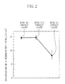
- FIG. 2 is a graph illustrating the polarization of a ferroelectric film, which was measured to evaluate the device according to the embodiment.
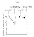
- FIG. 3 is a graph illustrating the polarization of a ferroelectric film, which was measured to evaluate a first method for fabricating the device according to the embodiment.
- FIG. 4 is a graph illustrating a relationship between the anneal temperature and the face-to-face distance of Pt (222) planes, which was analyzed to test the anneal temperatures by a second method for fabricating the device according to the embodiment.
- FIG. 5 is a cross-sectional view of a known semiconductor device.
- FIGS. 6A through 6F are cross-sectional views illustrating respective process steps of fabricating the known device.
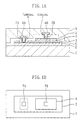
- FIG. 1A illustrates a cross-sectional structure of the device of this embodiment.
- a capacitor, formed on a semiconductor substrate 1 consists of: lower and upper electrodes 2 and 4 , each of which is made of a Pt film; and a capacitive insulating film 3 of a ferroelectric like SrBi 2 Ta 2 O 9 .
- a contact layer 5 made of TiN is formed on the upper electrode 4 .
- an insulating film 6 of silicon dioxide or nitride covers the lower and upper electrodes 2 and 4 , capacitive insulating film 3 and contact layer 5 .
- the lower electrode 2 is connected to a first metal interconnect 8A , which is formed on a part of the insulating film 6 and filled in a first contact hole 7A .
- the upper electrode 4 is connected to a second metal interconnect 8B , which is formed on another part of the insulating film 6 and filled in a second contact hole 7B .
- Each of the first and second metal interconnects 8A and 8B is made up of a lower titanium nitride film and an upper aluminum film. Also, a passivation film 9 made of silicon nitride is deposited over all the members described above.
- the contact layer 5 of TiN is formed on the upper electrode 4 . Therefore, almost none of the metal atoms in the contact layer 5 diffuses through the upper electrode 4 to reach the capacitive insulating film 3 , even if annealing is performed in a subsequent process step. Accordingly, electrical characteristic of the capacitor does not deteriorate because the polarization properties of the ferroelectric capacitive insulating film 3 do not degrade.
- the contact layer 5 does not exist inside the second contact hole 7B , which connects the second metal interconnect 8B to the upper electrode 4 . This is because the contact layer 5 is supposed to exist only partially between the upper electrode 4 and the insulating film 6 to such an extent that the insulating film 6 will not peel off the upper electrode 4 in a subsequent process step. Therefore, the contact layer 5 does not have to exist inside the second contact hole 7B .
- the TiN contact layer 5 is used in this embodiment.
- single-layer film made of a metal nitride like TaN, single-layer film made of a metal oxide such as TiO x , or multilayer structure made up of metal nitride and metal oxide films may also be used. This is because the metal atoms in the contact layer 5 will not diffuse either with any of these films even if annealing is performed in a subsequent process step.
- Ta behaves like Ti when diffusing.
- the first and known methods differ just in the composition of a contact layer and in the method of depositing the contact layer. Therefore, only the difference in the method of depositing the contact layer will be described.
- the first method is characterized in that the contact layer 5 is deposited by a sputtering process using a target of a metal nitride like TiN or a metal oxide such as TiO x .
- the contact layer 5 may be either a single-layer film made of a metal nitride or a metal oxide or a multilayer structure made up of metal oxide and metal nitride films.
- metal atoms e.g., Ti atoms
- the polarization properties of the capacitive insulating film 3 might degrade.
- a metal nitride or oxide film is deposited by a sputtering process using a target of a metal nitride or oxide, almost none of the metal atoms will diffuse into the upper electrode 4 . Therefore, the degradation in polarization of the capacitive insulating film 3 is much more likely to be suppressed.
- the polarization of the ferroelectric film with the TiN or TiO x contact layer deposited by the sputtering process was almost the same as that of the ferroelectric film with no contact layer shown in FIG. 2 .
- the polarization of the ferroelectric film with the contact layer formed by nitriding or oxidizing the Ti film is smaller than that of the ferroelectric film with the TiN or TiO x contact layer deposited by the sputtering process.
- the decrease of the polarization where the contact layer is formed by oxidizing the Ti film is smaller than that of the polarization where the contact layer is formed by nitriding the Ti film. This is because O atoms rapidly bond to Ti atoms to form Tio x when oxidation is performed, whereas N atoms do not bond rapidly to Ti atoms when nitriding is performed.
- a sputtering process is performed using a target of a metal nitride like TiN or a metal oxide such as TiO x to deposit a metal nitride or oxide film.
- sputtering may also be performed using a target of a metal nitride like TaN or a metal oxide such as TaO x to deposit another metal nitride or oxide film.
- a sputtering process is performed using a target of a metal nitride or oxide according to the first method.
- a reactive sputtering process may also be performed to deposit another metal nitride or oxide film within a N 2 or O 2 gas ambient using a target of a metal such as Ti or Ta.
- first metal film of Pt for example, ferroelectric film and second metal film of Pt, for instance, are formed in this order on the semiconductor substrate 1. Then, the second metal film, ferroelectric film and first metal film are patterned sequentially to form upper electrode, capacitive insulating film and lower electrode, respectively.
- annealing is performed at a temperature between 300°C and 800°C to relax the internal stress of the upper and lower electrodes and to shrink these electrodes.
- a contact layer of a metal nitride like TiN or a metal oxide such as TiO x is deposited on the upper electrode and patterned. Thereafter, an insulating film, contact holes and metal interconnects are formed as in the known process.
- the contact layer is deposited on the capacitor after the upper electrode of the capacitor has been shrunk by annealing the capacitor. Therefore, the upper electrode will not be shrunk anymore even if annealing is performed in a subsequent semiconductor process step. As a result, a void is unlikely to be formed in the upper electrode because stress applied to the upper electrode is lighter than usual.
- annealing is performed at a temperature between 300°C and 800°C after the capacitor, which is made up of the upper and lower electrodes and the capacitive insulating film, has been formed.
- the second metal film, which will form the upper electrode may be annealed at a temperature between 300°C and 800°C. In such an alternative embodiment, the same effects can also be obtained.
- the anneal temperature is preferably between 300°C and 800°C.
- FIG. 4 illustrates a relationship between the anneal temperature (°C) and the face-to-face distance (nm) between (222) Pt crystal planes. It can be seen from FIG. 4 that the higher the anneal temperature, the shorter the face-to-face distance and that the face-to-face distance decreased by about 3. 0 ⁇ 10 -4 nm when annealing was performed at about 300°C. It can also be seen from FIG. 4 that the decrease of the face-to-face distance converged when the anneal temperature was 600°C or more. Thus, it can be seen that the higher the anneal temperature, the shorter the interstitial distance of the Pt crystals and a Pt film for the upper and lower electrodes shrinks.
- the anneal temperature is preferably between 300°C and 800°C.
Landscapes
- Semiconductor Memories (AREA)
- Semiconductor Integrated Circuits (AREA)
- Ceramic Capacitors (AREA)
- Physical Deposition Of Substances That Are Components Of Semiconductor Devices (AREA)
Abstract

Description
- The present invention relates to a semiconductor device including a capacitor that has a capacitive insulating film formed out of a ferroelectric film, and also relates to a method for fabricating the device.
- In recent years, performance of consumer electronic units is being more and more enhanced, because microcomputers, for example, are now able to operate at much higher speeds with much lower power consumed. To cope with the performance enhancement, semiconductor elements in a semiconductor device have been miniaturized rapidly. Thus, unwanted radiation, i.e., electromagnetic noise generated from the electronic units, is a serious problem.
- To reduce the unwanted radiation, a technique of building a capacitor with large capacitance, in which a ferroelectric film with a high dielectric constant is used as a capacitive insulating film, in a semiconductor integrated circuit device, for example, is attracting much attention.
- Also, the number of dynamic RAMs (DRAMs) integrated on a chip goes on increasing. In response, a technique of using high-dielectric-constant materials instead of silicon oxides or silicon nitrides, which have been used widely, is now researched broadly.
- Further, a ferroelectric film exhibiting spontaneous polarization has also been researched and developed vigorously to implement a nonvolatile RAM that can operate with a lower voltage applied and that can also perform high-speed write and read operations.
- The most important problem to be solved in implementing a semiconductor device with a capacitor including a ferroelectric capacitive insulating film is increasing the number of DRAMs integrated on a chip without degrading the characteristic of the capacitor.
- In particular, to use noble metals (e.g., Pt, Ir and the like) as electrode materials for a ferroelectric capacitor is a brand-new technique developed over the past few years. Therefore, there are still many problems left to successfully apply this technique to semiconductor device processing for a capacitor including a ferroelectric capacitive insulating film. For example, adhesiveness of the electrode materials like Pt and Ir to an insulating film such as a silicon dioxide or silicon nitride film is not satisfactory. Therefore, the insulating film might peel off if annealing is performed at a high temperature. Also, depending on the type of the undercoat film, the insulating film might peel off right after the insulating film has been deposited. In view of these problems, a contact layer is needed between the Pt or Ir upper electrode and the insulating film of silicon dioxide or nitride. In the prior art, a titanium film, which has often been used in semiconductor device processing, is used as a contact layer.
- Hereinafter, a known semiconductor device and a method for fabricating the device will be described with reference to the accompanying drawings.
- FIG. 5 illustrates a cross-sectional structure of the principal portion of a known semiconductor device. As shown in FIG. 5, a
lower electrode 11, a capacitiveinsulating film 12, anupper electrode 13 and acontact layer 14 are formed in this order on thesemiconductor substrate 10. Each of the lower andupper electrodes insulating film 12 is formed out of a ferroelectric film, and thecontact layer 14 is made of a Ti film. And aninsulating film 15 made of silicon dioxide or silicon nitride, for example, is deposited over the lower andupper electrodes insulating film 12 andcontact layer 14. - The
lower electrode 11 is connected to afirst metal interconnect 17A, which is formed on a part of theinsulating film 15 and filled in afirst contact hole 16A. And theupper electrode 13 is connected to asecond metal interconnect 17B, which is formed on another part of theinsulting film 15 and filled in asecond contact hole 16B. Each of the first andsecond metal interconnects passivation film 18 of silicon nitride is deposited over all the members described above. - Hereinafter, a method for fabricating the known semiconductor device will be described with reference to FIGS. 6A through 6F.
- First, as shown in FIG. 6A,
first Pt film 11A,ferroelectric film 12A,second Pt film 13A andTi film 14A are deposited in this order over asemiconductor substrate 10. Then, the Ti andsecond Pt films contact layer 14 out of theTi film 14A and anupper electrode 13 out of thesecond Pt film 13A, respectively, as shown in FIG. 6B. - Next, the ferroelectric and
first Pt films insulating film 12 out of theferroelectric film 12A and alower electrode 11 out of thefirst Pt film 11A, respectively, as shown in FIG. 6C. - Subsequently, as shown in FIG. 6D, an opening 12a is formed in a region of the capacitive
insulating film 12 in which afirst contact hole 16A will be defined. Then, aninsulating film 15 is deposited over the entire surface of thesemiconductor substrate 10. Next, the first andsecond contact holes insulating film 15 to partially expose the lower andupper electrodes - The next step is depositing a multilayer structure consisting of a lower titanium nitride film and an upper aluminum film over the
insulating film 15 in such a manner that the first andsecond contact holes first metal interconnect 17A connected to thelower electrode 11 and thesecond metal interconnect 17B connected to theupper electrode 13, respectively, as shown in FIG. 6E. - Next, a
passivation film 18 of silicon nitride is deposited over the entire surface of thesemiconductor substrate 10. In this manner, the known semiconductor device as shown in FIG. 6F is obtained. Although not shown in the drawings, after making openings in thepassivation film 18, electrode pads connected to the first andsecond metal interconnects - After the
contact layer 14,upper electrode 13, capacitiveinsulating film 12 andlower electrode 11 are formed by patterning, annealing is usually performed to repair the damage caused by the patterning of the capacitiveinsulating film 12. - However, as a result of the annealing, Ti atoms that make up the
contact layer 14 might diffuse through column-like crystals of Pt in theupper electrode 13 to reach the ferroelectric capacitiveinsulating film 12. In that case, the polarization properties of the ferroelectric capacitiveinsulating film 12 might degrade and electrical characteristic of the capacitor including the capacitiveinsulating film 12 might deteriorate. - In addition, as a result of the annealing, the
contact layer 14 will expand, while theupper electrode 13 will shrink. Therefore, a void might be formed in theupper electrode 13 because stress is applied to theupper electrode 13. - A first object of the present invention is to suppress the degradation in polarization properties of a ferroelectric film for a capacitive insulating film.
- A second object of the present invention is to prevent a void from being formed in an upper electrode.
- To achieve the first object, an inventive semiconductor device includes: a lower electrode formed on a substrate; a capacitive insulating film formed out of a ferroelectric film on the lower electrode; an upper electrode formed on the capacitive insulating film; a contact layer formed on the upper electrode; an insulating film formed to cover the lower electrode, the capacitive insulating film, the upper electrode and the contact layer; a contact hole passing through the insulating film and the contact layer to reach the upper electrode; and a metal interconnect, which is defined on a part of the insulating film, filled in the contact hole and connected to the upper electrode. In the device, the contact layer is a single-layer film or a multilayer structure. The single-layer film is made of a metal oxide or a metal nitride. And the multilayer structure is made up of metal oxide and metal nitride films.
- In the inventive device, the contact layer exists between the upper electrode and the insulating film except the region where the contact hole is opened. And the contact layer is either a single-layer film made of a metal oxide or a metal nitride or a multilayer structure made up of metal oxide and metal nitride films. Therefore, the insulating film is unlikely to peel off the contact layer and metal atoms in the contact layer are unlikely to diffuse into the upper electrode even if annealing is performed in a subsequent process step. In that case, it is hard for the metal atoms in the contact layer to reach the ferroelectric capacitive insulating film. Thus, the degradation in polarization properties of the ferroelectric film can be avoided, and the electric characteristic of the capacitor does not deteriorate.
- In one embodiment of the present invention, the upper electrode preferably contains Pt or Ir, the metal oxide film is preferably made of an oxide of Ti or an oxide of Ta, and the metal nitride film is preferably made of a nitride of Ti or a nitride of Ta.
- In general, if the upper electrode contains Pt or Ir, the upper electrode is made of column-like crystals, and is likely to allow the metal atoms to diffuse easily. However, an oxide of Ti or Ta or a nitride of Ti or Ta is -unlikely to diffuse into the upper electrode. Therefore, the degradation in the polarization properties of the ferroelectric film can substantially be suppressed in such an embodiment.
- To achieve the first object, an inventive method for fabricating a semiconductor device includes the steps of: a) depositing a first metal film, a ferroelectric film, a second metal film and a single-layer film or a multilayer structure in this order on a substrate, the single-layer film being made of a metal oxide or a metal nitride, the multilayer structure being made up of metal oxide and metal nitride films; b) patterning the single-layer film or the multilayer structure to form a contact layer; c) patterning the second metal film to form an upper electrode; d) patterning the ferroelectric film to form a capacitive insulating film; e) patterning the first metal film to form a lower electrode; f) depositing an insulating film covering the lower electrode, the capacitive insulating film, the upper electrode and the contact layer; g) opening a contact hole that passes through the insulating film and the contact layer to reach the upper electrode; and h) defining a metal interconnect, which is filled in the contact hole and connected to the upper electrode, on a part of the insulating film.
- According to the inventive method, the contact layer exists between the upper electrode and the insulating film except the region where the contact hole will be opened. And the contact layer is either a single-layer film made of a metal oxide or a metal nitride or a multilayer structure made up of metal oxide and metal nitride films. Therefore, the insulating film is unlikely to peel off the contact layer, and metal atoms in the contact layer are unlikely to diffuse into the upper electrode even if annealing is performed in a subsequent process step. In that case, it is hard for the metal atoms in the contact layer to reach the ferroelectric capacitive insulating film. Thus, the degradation in polarization properties of the ferroelectric film can be avoided, and the electric characteristic of the capacitor does not deteriorate.
- In one embodiment of the present invention, the single-layer film or the multilayer structure is preferably deposited in the step a) by a sputtering process using a target of a metal oxide or a metal nitride or by a reactive sputtering process performed within an ambient containing oxygen gas or nitrogen gas.
- In this manner, it is possible to prevent the metal atoms in the contact layer from diffusing into the upper electrode before bonding to oxygen atoms or nitrogen atoms. Therefore, the degradation in polarization properties of the ferroelectric capacitive insulating film is much more likely to be suppressed.
- To achieve the second object, the inventive method for fabricating a semiconductor device preferably further includes the step of annealing the second metal film at a temperature between 300°C and 800°C.
- In this manner, the contact layer is deposited on the capacitor after the second metal film, which will form the upper electrode, has been shrunk. Therefore, the upper electrode will not be shrunk anymore even if annealing is performed in a subsequent semiconductor process step. As a result, stress applied to the upper electrode is lighter than usual, and a void is unlikely to be formed in the upper electrode. In this case, the second metal film, which will form the upper electrode, is most likely to be shrunk because annealing is performed at 300°C or more, and formation of a hillock in the first and second metal films can be prevented because the anneal temperature is 800°C or less.
- FIG. 1A is a cross-sectional view of a semiconductor device according to an embodiment of the present invention, and FIG. 1B is a plan view of the device.
- FIG. 2 is a graph illustrating the polarization of a ferroelectric film, which was measured to evaluate the device according to the embodiment.
- FIG. 3 is a graph illustrating the polarization of a ferroelectric film, which was measured to evaluate a first method for fabricating the device according to the embodiment.
- FIG. 4 is a graph illustrating a relationship between the anneal temperature and the face-to-face distance of Pt (222) planes, which was analyzed to test the anneal temperatures by a second method for fabricating the device according to the embodiment.
- FIG. 5 is a cross-sectional view of a known semiconductor device.
- FIGS. 6A through 6F are cross-sectional views illustrating respective process steps of fabricating the known device.
- Hereinafter, a semiconductor device according to a preferred embodiment of the present invention will be described with reference to the accompanying drawings.
- FIG. 1A illustrates a cross-sectional structure of the device of this embodiment. A capacitor, formed on a
semiconductor substrate 1, consists of: lower andupper electrodes film 3 of a ferroelectric like SrBi2Ta2O9. - A
contact layer 5 made of TiN is formed on theupper electrode 4. And an insulating film 6 of silicon dioxide or nitride covers the lower andupper electrodes film 3 andcontact layer 5. - The
lower electrode 2 is connected to afirst metal interconnect 8A, which is formed on a part of the insulating film 6 and filled in afirst contact hole 7A. And theupper electrode 4 is connected to asecond metal interconnect 8B, which is formed on another part of the insulating film 6 and filled in asecond contact hole 7B. Each of the first andsecond metal interconnects passivation film 9 made of silicon nitride is deposited over all the members described above. - According to this embodiment, the
contact layer 5 of TiN is formed on theupper electrode 4. Therefore, almost none of the metal atoms in thecontact layer 5 diffuses through theupper electrode 4 to reach the capacitive insulatingfilm 3, even if annealing is performed in a subsequent process step. Accordingly, electrical characteristic of the capacitor does not deteriorate because the polarization properties of the ferroelectric capacitive insulatingfilm 3 do not degrade. - In this embodiment, the
contact layer 5 does not exist inside thesecond contact hole 7B, which connects thesecond metal interconnect 8B to theupper electrode 4. This is because thecontact layer 5 is supposed to exist only partially between theupper electrode 4 and the insulating film 6 to such an extent that the insulating film 6 will not peel off theupper electrode 4 in a subsequent process step. Therefore, thecontact layer 5 does not have to exist inside thesecond contact hole 7B. - We measured the polarization of the ferroelectric film to evaluate the effects of this embodiment. The results of the measurement will be described with reference to the drawings. We used capacitor with no contact layer, capacitor with a contact layer of TiN, and capacitor with a contact layer of Ti as samples for the measurement. None of these capacitors had the insulating film 6, first and
second contact holes second metal interconnects passivation film 9. We measured the polarization of the ferroelectric film at the terminalsA and B shown in FIG. 1A. - The polarization of the capacitor with the TiN contact layer and that of the capacitor with no contact layer, which was hardly affected by diffused Ti atoms, were at almost the same levels as shown in FIG. 2. Specifically, the polarization of these capacitors measured 14 µC/cm2 or more, and a variation of 1.5 µC/cm2 or less was observed. In contrast, the capacitor with the Ti contact layer showed a polarization of about 8 µC/cm2 and a variation of 3µC/cm2.
- We ascertained from those results that it is possible to prevent the metal atoms in the
contact layer 5 from diffusing and thereby suppress the degradation in polarization of the ferroelectric capacitive insulatingfilm 3 by using the capacitor of this embodiment, even if annealing is performed in a subsequent process step of a semiconductor process. - It should be noted that the
TiN contact layer 5 is used in this embodiment. Alternatively, single-layer film made of a metal nitride like TaN, single-layer film made of a metal oxide such as TiOx, or multilayer structure made up of metal nitride and metal oxide films may also be used. This is because the metal atoms in thecontact layer 5 will not diffuse either with any of these films even if annealing is performed in a subsequent process step. It should also be noted that Ta behaves like Ti when diffusing. - Hereinafter, a first method for fabricating the device according to the embodiment will be described. The first and known methods differ just in the composition of a contact layer and in the method of depositing the contact layer. Therefore, only the difference in the method of depositing the contact layer will be described.
- The first method is characterized in that the
contact layer 5 is deposited by a sputtering process using a target of a metal nitride like TiN or a metal oxide such as TiOx. Thecontact layer 5 may be either a single-layer film made of a metal nitride or a metal oxide or a multilayer structure made up of metal oxide and metal nitride films. - Hereinafter, it will be described what is the difference between depositing a metal nitride or oxide film by a sputtering process using a target of a metal nitride or oxide and depositing a metal film like a Ti film and then nitriding or oxidizing the film.
- If a metal film is nitrided or oxidized to form a metal nitride or oxide film, metal atoms (e.g., Ti atoms) in the metal film might diffuse into the
upper electrode 4 before bonding to nitrogen or oxygen atoms. Therefore, the polarization properties of the capacitive insulatingfilm 3 might degrade. In contrast, if a metal nitride or oxide film is deposited by a sputtering process using a target of a metal nitride or oxide, almost none of the metal atoms will diffuse into theupper electrode 4. Therefore, the degradation in polarization of the capacitive insulatingfilm 3 is much more likely to be suppressed. - We measured the polarization of a ferroelectric film to evaluate the first method. The results of the measurement will be described with reference to FIG. 3. We used four capacitors as samples for the measurement. Specifically, we used a capacitor with a contact layer of TiN deposited by a sputtering process and a capacitor with a contact layer of TiN formed by nitriding a Ti film. We also used a capacitor with a contact layer of TiOx deposited by a sputtering process and a capacitor with a contact layer of TiOx formed by oxidizing a Ti film.
- As shown in FIG. 3, the polarization of the ferroelectric film with the TiN or TiOx contact layer deposited by the sputtering process was almost the same as that of the ferroelectric film with no contact layer shown in FIG. 2. However, the polarization of the ferroelectric film with the contact layer formed by nitriding or oxidizing the Ti film is smaller than that of the ferroelectric film with the TiN or TiOx contact layer deposited by the sputtering process. Further, the decrease of the polarization where the contact layer is formed by oxidizing the Ti film is smaller than that of the polarization where the contact layer is formed by nitriding the Ti film. This is because O atoms rapidly bond to Ti atoms to form Tiox when oxidation is performed, whereas N atoms do not bond rapidly to Ti atoms when nitriding is performed.
- According to the first method, a sputtering process is performed using a target of a metal nitride like TiN or a metal oxide such as TiOx to deposit a metal nitride or oxide film. Alternatively, sputtering may also be performed using a target of a metal nitride like TaN or a metal oxide such as TaOx to deposit another metal nitride or oxide film.
- In addition, a sputtering process is performed using a target of a metal nitride or oxide according to the first method. Alternatively, a reactive sputtering process may also be performed to deposit another metal nitride or oxide film within a N2 or O2 gas ambient using a target of a metal such as Ti or Ta.
- Hereinafter, a second method for fabricating the device according to the embodiment will be described.
- First, first metal film of Pt, for example, ferroelectric film and second metal film of Pt, for instance, are formed in this order on the
semiconductor substrate 1. Then, the second metal film, ferroelectric film and first metal film are patterned sequentially to form upper electrode, capacitive insulating film and lower electrode, respectively. - Next, annealing is performed at a temperature between 300°C and 800°C to relax the internal stress of the upper and lower electrodes and to shrink these electrodes. Then, a contact layer of a metal nitride like TiN or a metal oxide such as TiOx is deposited on the upper electrode and patterned. Thereafter, an insulating film, contact holes and metal interconnects are formed as in the known process.
- According to the second method, the contact layer is deposited on the capacitor after the upper electrode of the capacitor has been shrunk by annealing the capacitor. Therefore, the upper electrode will not be shrunk anymore even if annealing is performed in a subsequent semiconductor process step. As a result, a void is unlikely to be formed in the upper electrode because stress applied to the upper electrode is lighter than usual.
- According to the second method, annealing is performed at a temperature between 300°C and 800°C after the capacitor, which is made up of the upper and lower electrodes and the capacitive insulating film, has been formed. Alternatively, the second metal film, which will form the upper electrode, may be annealed at a temperature between 300°C and 800°C. In such an alternative embodiment, the same effects can also be obtained.
- Hereinafter, it will be described why the anneal temperature is preferably between 300°C and 800°C.
- FIG. 4 illustrates a relationship between the anneal temperature (°C) and the face-to-face distance (nm) between (222) Pt crystal planes. It can be seen from FIG. 4 that the higher the anneal temperature, the shorter the face-to-face distance and that the face-to-face distance decreased by about 3. 0×10-4nm when annealing was performed at about 300°C. It can also be seen from FIG. 4 that the decrease of the face-to-face distance converged when the anneal temperature was 600°C or more. Thus, it can be seen that the higher the anneal temperature, the shorter the interstitial distance of the Pt crystals and a Pt film for the upper and lower electrodes shrinks.
- Furthermore, we analyzed a relationship between the anneal temperature and the formation of a void, and we found that the formation of a void can be suppressed if the anneal temperature is 300°C or more. We also found that a hillock will be formed if annealing is performed at a relatively high temperature of 800°C or more.
- For these reasons, the anneal temperature is preferably between 300°C and 800°C.
Claims (5)
- A semiconductor device comprising:wherein the contact layer is a single-layer film or a multilayer structure, the single-layer film being made of a metal oxide or a metal nitride, the multilayer structure being made up of metal oxide and metal nitride films.a lower electrode formed on a substrate;a capacitive insulating film formed out of a ferroelectric film on the lower electrode;an upper electrode formed on the capacitive insulating film;a contact layer formed on the upper electrode;an insulating film formed to cover the lower electrode, the capacitive insulating film, the upper electrode and the contact layer;a contact hole passing through the insulating film and the contact layer to reach the upper electrode; anda metal interconnect, which is defined on a part of the insulating film, filled in the contact hole and connected to the upper electrode,
- The device of Claim 1, wherein the upper electrode contains Pt or Ir, and
wherein the metal oxide film is made of an oxide of Ti or an oxide of Ta, while the metal nitride film is made of a nitride of Ti or a nitride of Ta. - A method for fabricating a semiconductor device, comprising the steps of:a) depositing a first metal film, a ferroelectric film, a second metal film and a single-layer film or a multilayer structure in this order on a substrate, the single-layer film being made of a metal oxide or a metal nitride, the multilayer structure being made up of metal oxide and metal nitride films;b) patterning the single-layer film or the multilayer structure to form a contact layer;c) patterning the second metal film to form an upper electrode;d) patterning the ferroelectric film to form a capacitive insulating film;e) patterning the first metal film to form a lower electrode;f) depositing an insulating film covering the lower electrode, the capacitive insulating film, the upper electrode and the contact layer;g) opening a contact hole that passes through the insulating film and the contact layer to reach the upper electrode; andh) defining a metal interconnect, which is filled in the contact hole and connected to the upper electrode, on a part of the insulating film.
- The device of Claim 3, wherein in the step a), the single-layer film or the multilayer structure is deposited by a sputtering process using a target of a metal oxide or a metal nitride or by a reactive sputtering process performed within an ambient containing oxygen gas or nitrogen gas.
- The method of Claim 3, further comprising the step of annealing the second metal film at a temperature between 300°C and 800°C.
Applications Claiming Priority (2)
| Application Number | Priority Date | Filing Date | Title |
|---|---|---|---|
| JP35310499A JP3276351B2 (en) | 1999-12-13 | 1999-12-13 | Method for manufacturing semiconductor device |
| JP35310499 | 1999-12-13 |
Publications (1)
| Publication Number | Publication Date |
|---|---|
| EP1109223A1 true EP1109223A1 (en) | 2001-06-20 |
Family
ID=18428601
Family Applications (1)
| Application Number | Title | Priority Date | Filing Date |
|---|---|---|---|
| EP00125794A Withdrawn EP1109223A1 (en) | 1999-12-13 | 2000-11-24 | Semiconductor device and method for fabricating the same |
Country Status (5)
| Country | Link |
|---|---|
| US (1) | US6960800B2 (en) |
| EP (1) | EP1109223A1 (en) |
| JP (1) | JP3276351B2 (en) |
| KR (1) | KR100658259B1 (en) |
| TW (1) | TW476077B (en) |
Cited By (1)
| Publication number | Priority date | Publication date | Assignee | Title |
|---|---|---|---|---|
| WO2004021414A3 (en) * | 2002-08-12 | 2004-07-29 | Infineon Technologies Ag | Integrated circuit arrangements, in particular capacitor arrangements and corresponding production method |
Families Citing this family (9)
| Publication number | Priority date | Publication date | Assignee | Title |
|---|---|---|---|---|
| TW460748B (en) * | 1998-05-26 | 2001-10-21 | Matsushita Electronics Corp | Capacitor and method for fabricating the same |
| JP2003100887A (en) * | 2001-09-26 | 2003-04-04 | Nec Corp | Semiconductor device |
| KR100449250B1 (en) * | 2002-01-07 | 2004-09-18 | 주식회사 하이닉스반도체 | Method for forming bit line of semiconductor device |
| JP2008016490A (en) * | 2006-07-03 | 2008-01-24 | Nec Electronics Corp | Semiconductor device |
| JP5098422B2 (en) * | 2007-04-27 | 2012-12-12 | 株式会社村田製作所 | Thin film electronic components |
| JP2009010114A (en) * | 2007-06-27 | 2009-01-15 | Murata Mfg Co Ltd | Dielectric thin film capacitor |
| WO2018198330A1 (en) * | 2017-04-28 | 2018-11-01 | ゼンテルジャパン株式会社 | Capacitor device and manufacturing method therefor |
| US12317521B2 (en) | 2017-04-28 | 2025-05-27 | AP Memory Technology Corp. | Capacitor device and manufacturing method therefor |
| CN115943470B (en) * | 2020-06-29 | 2025-11-14 | Tdk株式会社 | Thin-film capacitors and electronic circuit boards incorporating them |
Citations (3)
| Publication number | Priority date | Publication date | Assignee | Title |
|---|---|---|---|---|
| US5475248A (en) * | 1990-09-28 | 1995-12-12 | Ramtron International Corporation | Semiconductor device with a conductive reaction-preventing film |
| EP0766319A2 (en) * | 1995-09-29 | 1997-04-02 | Sony Corporation | Capacitor having ferroelectric film for nonvolatile memory cell, and method of manufacturing the same |
| EP0933783A2 (en) * | 1998-01-29 | 1999-08-04 | Sharp Kabushiki Kaisha | Nonvolatile semiconductor storage device using ferroelectric films and its fabricating method. |
Family Cites Families (9)
| Publication number | Priority date | Publication date | Assignee | Title |
|---|---|---|---|---|
| JPH09246082A (en) | 1996-03-13 | 1997-09-19 | Matsushita Electron Corp | Capacitance element and method of manufacturing |
| JPH09280947A (en) | 1996-04-11 | 1997-10-31 | Matsushita Electric Ind Co Ltd | Ferroelectric element |
| JPH11145410A (en) | 1997-11-13 | 1999-05-28 | Toshiba Corp | Semiconductor device and manufacturing method thereof |
| JP3212930B2 (en) * | 1997-11-26 | 2001-09-25 | 日本電気株式会社 | Capacity and manufacturing method thereof |
| JPH11307733A (en) | 1998-04-17 | 1999-11-05 | Nec Corp | Manufacturing method of ferroelectric integrated circuit |
| KR100279297B1 (en) * | 1998-06-20 | 2001-02-01 | 윤종용 | Semiconductor device and manufacturing method thereof |
| KR100292819B1 (en) * | 1998-07-07 | 2001-09-17 | 윤종용 | Capacitor and manufacturing method thereof |
| US6586790B2 (en) * | 1998-07-24 | 2003-07-01 | Kabushiki Kaisha Toshiba | Semiconductor device and method for manufacturing the same |
| JP2000138350A (en) * | 1998-10-30 | 2000-05-16 | Sharp Corp | Method for manufacturing semiconductor memory device |
-
1999
- 1999-12-13 JP JP35310499A patent/JP3276351B2/en not_active Expired - Fee Related
-
2000
- 2000-10-20 TW TW089122111A patent/TW476077B/en not_active IP Right Cessation
- 2000-10-27 KR KR1020000063548A patent/KR100658259B1/en not_active Expired - Fee Related
- 2000-11-24 EP EP00125794A patent/EP1109223A1/en not_active Withdrawn
- 2000-12-12 US US09/734,176 patent/US6960800B2/en not_active Expired - Fee Related
Patent Citations (3)
| Publication number | Priority date | Publication date | Assignee | Title |
|---|---|---|---|---|
| US5475248A (en) * | 1990-09-28 | 1995-12-12 | Ramtron International Corporation | Semiconductor device with a conductive reaction-preventing film |
| EP0766319A2 (en) * | 1995-09-29 | 1997-04-02 | Sony Corporation | Capacitor having ferroelectric film for nonvolatile memory cell, and method of manufacturing the same |
| EP0933783A2 (en) * | 1998-01-29 | 1999-08-04 | Sharp Kabushiki Kaisha | Nonvolatile semiconductor storage device using ferroelectric films and its fabricating method. |
Cited By (1)
| Publication number | Priority date | Publication date | Assignee | Title |
|---|---|---|---|---|
| WO2004021414A3 (en) * | 2002-08-12 | 2004-07-29 | Infineon Technologies Ag | Integrated circuit arrangements, in particular capacitor arrangements and corresponding production method |
Also Published As
| Publication number | Publication date |
|---|---|
| JP2001168290A (en) | 2001-06-22 |
| JP3276351B2 (en) | 2002-04-22 |
| KR20010067373A (en) | 2001-07-12 |
| US6960800B2 (en) | 2005-11-01 |
| US20020030243A1 (en) | 2002-03-14 |
| KR100658259B1 (en) | 2006-12-14 |
| TW476077B (en) | 2002-02-11 |
Similar Documents
| Publication | Publication Date | Title |
|---|---|---|
| US5396095A (en) | Method of manufacturing a semiconductor device comprising a capacitor with a ferroelectric dielectric, and semiconductor device comprising such a capacitor | |
| US5929475A (en) | Capacitor for integrated circuit and its fabrication method | |
| JP3252835B2 (en) | Semiconductor device and manufacturing method thereof | |
| US6723637B2 (en) | Semiconductor device and method for fabricating the same | |
| US6265260B1 (en) | Method for making an integrated circuit capacitor including tantalum pentoxide | |
| US6166424A (en) | Capacitance structure for preventing degradation of the insulating film | |
| US6426306B1 (en) | Barrier layer fabrication methods | |
| US5742472A (en) | Stacked capacitors for integrated circuit devices and related methods | |
| JP2917916B2 (en) | Semiconductor integrated circuit using ferroelectric and method of manufacturing the same | |
| US6960800B2 (en) | Semiconductor device and method for fabricating the same | |
| KR100391987B1 (en) | semiconductor devices having ferroelectric material capacitor and method of making the same | |
| US20040089891A1 (en) | Semiconductor device including electrode or the like having opening closed and method of manufacturing the same | |
| JP2846310B1 (en) | Semiconductor device and manufacturing method thereof | |
| JPH0837282A (en) | Capacitive device, semiconductor device and manufacture thereof | |
| US6818500B2 (en) | Method of making a memory cell capacitor with Ta2O5 dielectric | |
| JPH0992795A (en) | Capacitance element, manufacturing method thereof, and semiconductor device | |
| US20030132472A1 (en) | Semiconductor device with a ferroelectric memory provided on a semiconductor substrate | |
| JP2907767B2 (en) | Method for manufacturing semiconductor device | |
| US6232131B1 (en) | Method for manufacturing semiconductor device with ferroelectric capacitors including multiple annealing steps | |
| US6238932B1 (en) | Method for fabricating reliable multilayer bottom electrode for ferroelectric capacitors | |
| US20040197984A1 (en) | Adhesion layer for Pt on SiO2 | |
| JPH04349657A (en) | Semiconductor device | |
| US6839220B1 (en) | Multi-layer barrier allowing recovery anneal for ferroelectric capacitors | |
| US6355516B1 (en) | Method of manufacturing a capacitor with a bi-layer Ta2O5 capacitor dielectric in a semiconductor device including performing a plasma treatment on the first Ta2O5 layer |
Legal Events
| Date | Code | Title | Description |
|---|---|---|---|
| PUAI | Public reference made under article 153(3) epc to a published international application that has entered the european phase |
Free format text: ORIGINAL CODE: 0009012 |
|
| AK | Designated contracting states |
Kind code of ref document: A1 Designated state(s): DE FR GB |
|
| AX | Request for extension of the european patent |
Free format text: AL;LT;LV;MK;RO;SI |
|
| RAP1 | Party data changed (applicant data changed or rights of an application transferred) |
Owner name: MATSUSHITA ELECTRIC INDUSTRIAL CO., LTD. |
|
| 17P | Request for examination filed |
Effective date: 20010806 |
|
| AKX | Designation fees paid |
Free format text: DE FR GB |
|
| RAP1 | Party data changed (applicant data changed or rights of an application transferred) |
Owner name: PANASONIC CORPORATION |
|
| STAA | Information on the status of an ep patent application or granted ep patent |
Free format text: STATUS: THE APPLICATION IS DEEMED TO BE WITHDRAWN |
|
| 18D | Application deemed to be withdrawn |
Effective date: 20100601 |