EP1108552B1 - Thermokopf, thermokopfeinheit und herstellungsverfahren dafür - Google Patents
Thermokopf, thermokopfeinheit und herstellungsverfahren dafür Download PDFInfo
- Publication number
- EP1108552B1 EP1108552B1 EP99937006A EP99937006A EP1108552B1 EP 1108552 B1 EP1108552 B1 EP 1108552B1 EP 99937006 A EP99937006 A EP 99937006A EP 99937006 A EP99937006 A EP 99937006A EP 1108552 B1 EP1108552 B1 EP 1108552B1
- Authority
- EP
- European Patent Office
- Prior art keywords
- wiring substrate
- thermal head
- chip
- head
- head chip
- Prior art date
- Legal status (The legal status is an assumption and is not a legal conclusion. Google has not performed a legal analysis and makes no representation as to the accuracy of the status listed.)
- Expired - Lifetime
Links
Images


Classifications
-
- B—PERFORMING OPERATIONS; TRANSPORTING
- B41—PRINTING; LINING MACHINES; TYPEWRITERS; STAMPS
- B41J—TYPEWRITERS; SELECTIVE PRINTING MECHANISMS, i.e. MECHANISMS PRINTING OTHERWISE THAN FROM A FORME; CORRECTION OF TYPOGRAPHICAL ERRORS
- B41J2/00—Typewriters or selective printing mechanisms characterised by the printing or marking process for which they are designed
- B41J2/315—Typewriters or selective printing mechanisms characterised by the printing or marking process for which they are designed characterised by selective application of heat to a heat sensitive printing or impression-transfer material
- B41J2/32—Typewriters or selective printing mechanisms characterised by the printing or marking process for which they are designed characterised by selective application of heat to a heat sensitive printing or impression-transfer material using thermal heads
- B41J2/335—Structure of thermal heads
- B41J2/33505—Constructional details
- B41J2/3351—Electrode layers
-
- B—PERFORMING OPERATIONS; TRANSPORTING
- B41—PRINTING; LINING MACHINES; TYPEWRITERS; STAMPS
- B41J—TYPEWRITERS; SELECTIVE PRINTING MECHANISMS, i.e. MECHANISMS PRINTING OTHERWISE THAN FROM A FORME; CORRECTION OF TYPOGRAPHICAL ERRORS
- B41J2/00—Typewriters or selective printing mechanisms characterised by the printing or marking process for which they are designed
- B41J2/315—Typewriters or selective printing mechanisms characterised by the printing or marking process for which they are designed characterised by selective application of heat to a heat sensitive printing or impression-transfer material
- B41J2/32—Typewriters or selective printing mechanisms characterised by the printing or marking process for which they are designed characterised by selective application of heat to a heat sensitive printing or impression-transfer material using thermal heads
- B41J2/335—Structure of thermal heads
- B41J2/33575—Processes for assembling process heads
-
- B—PERFORMING OPERATIONS; TRANSPORTING
- B41—PRINTING; LINING MACHINES; TYPEWRITERS; STAMPS
- B41J—TYPEWRITERS; SELECTIVE PRINTING MECHANISMS, i.e. MECHANISMS PRINTING OTHERWISE THAN FROM A FORME; CORRECTION OF TYPOGRAPHICAL ERRORS
- B41J2/00—Typewriters or selective printing mechanisms characterised by the printing or marking process for which they are designed
- B41J2/315—Typewriters or selective printing mechanisms characterised by the printing or marking process for which they are designed characterised by selective application of heat to a heat sensitive printing or impression-transfer material
- B41J2/32—Typewriters or selective printing mechanisms characterised by the printing or marking process for which they are designed characterised by selective application of heat to a heat sensitive printing or impression-transfer material using thermal heads
- B41J2/335—Structure of thermal heads
- B41J2/3359—Manufacturing processes
-
- B—PERFORMING OPERATIONS; TRANSPORTING
- B41—PRINTING; LINING MACHINES; TYPEWRITERS; STAMPS
- B41J—TYPEWRITERS; SELECTIVE PRINTING MECHANISMS, i.e. MECHANISMS PRINTING OTHERWISE THAN FROM A FORME; CORRECTION OF TYPOGRAPHICAL ERRORS
- B41J2/00—Typewriters or selective printing mechanisms characterised by the printing or marking process for which they are designed
- B41J2/315—Typewriters or selective printing mechanisms characterised by the printing or marking process for which they are designed characterised by selective application of heat to a heat sensitive printing or impression-transfer material
- B41J2/32—Typewriters or selective printing mechanisms characterised by the printing or marking process for which they are designed characterised by selective application of heat to a heat sensitive printing or impression-transfer material using thermal heads
- B41J2/345—Typewriters or selective printing mechanisms characterised by the printing or marking process for which they are designed characterised by selective application of heat to a heat sensitive printing or impression-transfer material using thermal heads characterised by the arrangement of resistors or conductors
Definitions
- the present invention relates to a thermal head and a thermal head unit, which are used, for instance, in a miniature portable recording apparatus, a facsimile machine, a printer for tickets and receipts, etc, and also relates to a method of manufacturing the thermal head and the thermal head unit.
- a thermal head includes a head chip in which heating elements arrayed in a row and electrodes connected to these elements are provided on a ceramic substrate, and an IC chip serving as a driver for outputting print signals to selectively generate heat from desired heating elements at desired timings.
- Fig. 19 shows an example of a thermal head unit in which the thermal head of this type is mounted onto a heat radiating plate to form a unit.
- the thermal head unit includes a thermal head 101, and a heat radiating plate 102 made of aluminum or the like.
- the thermal head 101 is designed such that an electrode 104 and a heating element 105 are formed on a ceramic substrate 103, and an IC chip 106 is further mounted thereon.
- the electrode 104, a separately provided external terminal 107 for inputting external signals therein, and the IC chip 106 are connected together through bonding wires 108.
- the IC chip 106 and the bonding wires 108 are molded with sealing resin 109.
- a relatively large ceramic substrate 103 is used, and the electrodes 104, the heating elements 105 and the like are formed as thin or thick films on the substrate 103. For this reason, the board obtained by one board forming process is low in number, and thus the productivity is low.
- a composite substrate using a ceramic substrate reduced in size that is, as shown in Fig. 20, in place of the ceramic substrate 103, a ceramic circuit board 103A and a wiring substrate 103B such as a glass fabric based epoxy resin substrate (hereafter referred to as GE substrate when applicable) are used. In this case, the external terminal 107 is provided on the wiring substrate 103B.
- a ceramic circuit board 103A and a wiring substrate 103B such as a glass fabric based epoxy resin substrate (hereafter referred to as GE substrate when applicable) are used.
- the external terminal 107 is provided on the wiring substrate 103B.
- European Patent Publication No. 0513660 discloses a thermal printing head comprising a ceramic base board and a ceramic head board.
- the upper surface of the head board is formed with a thin glaze layer.
- the upper surface of the glaze layer is formed with a heating resistor line, common electrode and individual electrodes in conduction with the heat resisting line.
- the upper surface of the base board also directly carries drive ICs and a wiring conductor pattern for connecting the drive ICs to input terminals.
- the drive ICs are electrically connected to the wiring conductor pattern and the individual electrode through raised metallic wires.
- the array of drive ICs together with the wires are entirely enclosed in a resinous package.
- Japanese Utility Model 5009941 discloses a thermal print head comprising an alumina substrate in which an exoergic resistor and an electric conduction pattern are formed A printed wired board is pasted onto the substrate. A drive IC is carried in the printed wire board. The drive IC is connected to the electric conduction pattern and the printed wired board by wiring bonding. The drive IC is protected by a resin.
- an object of the present invention is to provide a thermal head unit and a method of manufacturing the same, which can improve the productivity of a board forming process while improving the handling ability of a mounting process, thereby remarkably reducing the cost.
- a thermal head unit comprising a thermal head mounted to a support member.
- the thermal head comprises a head chip having one surface on which heating elements and electrodes connected to the heating elements are provided, a wiring substrate joined to the other surface of the head chip and a semiconductor integrated circuit connected to the electrodes, the semiconductor integrated circuit being mounted to the wiring substrate, and wherein one end portion of the head chip, which serves as a heating element forming portion, is protruded from the wiring substrate.
- the support member is formed with an upper step portion to which the heating element forming portion is joined, and a step difference portion.
- the head unit is characterized in that the step difference portion is recessed more deeply from the upper step portion than a thickness of the wiring substrate, and an adhesive agent layer is provided in a clearance that is formed between the step difference portion and the wiring substrate when the heating element forming portion of the head chip is joined to the upper step portion.
- a thermal head unit according to the first aspect of the invention is characterised in that an adhesive layer is provided for joining the heating element forming portion of the head chip to the upper step portion.
- a thermal head unit according to any one of the first to second aspect of the invention is characterized in that an adhesive layer is provided for joining the heating element forming portion of the head chip to the upper step portion, and the adhesive agent layer is thicker than the adhesive layer.
- a thermal head unit according to any one of the first to third H aspects of the invention is further characterized in that at least one recessed groove is provided to a bottom portion of the step difference portion.
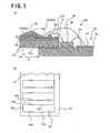
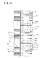
- Fig. 1 is a sectional schematic view and a major portion plane view of a thermal head according to an embodiment of the present invention.
- a thermal head 10 includes a head chip 20 formed with a plurality of thin film layers, and a wiring substrate 30 onto which the head chip 20 is stuck and joined.
- the head chip 20 is arranged such that the various thin film layers are formed on a ceramic substrate 21.
- An under coat layer 23 and a grace layer 22 made of a glass group material having a function of a thermally insulative layer are formed on the ceramic substrate 21.
- the grace layer 22 has a protruded rib 22a having a semicircular shape in section, which is located at a predetermined distance from one end of the ceramic substrate 21.
- heating elements 24 Formed on the area confronted with this protruded rib 22a are heating elements 24 intermittently arranged at predetermined intervals in the longitudinal direction thereof.
- Electrode 25, made of a metal such as an aluminum, are formed to contact end portions (left and right end portions in the drawing) of the respective heating elements 24 of the ceramic substrate 21. Further, a protective layer 28 is formed on the heating elements 24.
- each of the heating elements 24 is made up of a pair of heating elements 24a and 24b, and electrodes 25a and 25b are connected to respective end portions of the heating elements 24a and 24b.
- the electrode 25a serves as a segment electrode, and the end portion thereof is connected to a terminal portion 26 made, for instance, of a gold thin film layer.
- the electrode 25b serves as a common electrode, which is connected to a common electrode 27 that is located on an end portion of the substrate opposite from the heating elements 24. Further, the other end portions of the heating element 25a and 25b are connected to each other through a U-shaped electrode 25c.
- the wiring substrate 30 is arranged such that IC chips 32 and external terminals 33 are provided on a substrate 31 such as a GE substrate.
- the IC chip 32 serves as a driver for outputting drive signals to selectively generate heat from the desired heating elements 24.
- the IC chip 32 is provided for each of predetermined physical blocks of the heating elements 24.
- the external terminal 33 serves to input external signals into the respective IC chips 32.
- the IC chips 32 are connected to the terminal portions 26 and the external terminals 33 through bonding wires 34, respectively.
- the IC chips 32 and the bonding wires 34 are molded with sealing resin 35.
- the thermal head 10 described above is arranged such that the head chip 20 and the wiring substrate 30 serving as a support substrate for the head chip 20 are partially overlapped and jointed to each other so that the IC chip 32 is mounted on the wiring substrate 30. Accordingly, the width (in the right and left direction in the drawing) of the head chip 20 can be remarkably reduced, and therefore the number of the head chips 20 obtained during the board forming process can be increased to improve the productivity. Further, since the head chip 20 and the wiring substrate 30 can be handled in a state that they are joined to each other, the handling ability during the IC chip 32 mounting process is not be lowered.
- the handling ability can be further remarkably increased if the IC chip 32 mounting process and the wire bonding are carried out such that a plurality of head chips 20 are joined onto a wiring substrate forming plate from which a plurality of wiring substrates 30 can be dividingly obtained.
- the present invention will be described in further detail by taking an example of a manufacturing process for the thermal head 10 described above.
- the operation of a board forming process is basically not different from that in the background art, and therefore will not be described in detail. Note that since the head chip 20 is made small in size, the number of the head chip 20 obtained by one process can be remarkably increased, and thus the productivity can be improved largely.
- Fig. 2 is a plane view showing an initial stage of the mounting process
- Fig. 3 is a sectional view schematically showing substantially all of the mounting process.
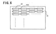
- a plurality of the head chips 20 are joined to a wiring substrate forming plate 41.
- the wiring substrate forming plate 41 is formed with elongated holes 42 corresponding to locations where the respective head chips 20 are to be joined.
- the elongated hole 42 is larger in length than the length of the head chip 20, and smaller in width than a protruded length (shown by H in Fig. 1 (a)) by which the head chip 20 is protruded from the wiring substrate 30.
- the end of the head chip 20 in the heating element side is disposed to extend along the width direction of the elongated hole 42, and the peripheral edge portion of the elongated hole 42 in the leading end side of the head chip 20 are not joined to the head chip 20. That is, in Fig.
- the elongated hole 42 and the head chip 20 are not joined to each other at a boundary 43a between the left side peripheral edge portion of the elongated hole 42 and the head chip 20, and are jointed to each other at a boundary 43b between the right side peripheral edge portion thereof and the head chip 20. Accordingly, when the wiring substrate forming plate 41 are divided into the wiring substrates 30 using the elongated holes 42, an inner peripheral surface 42a of the elongated hole 42 in one side of the width direction forms one end surface of the wiring substrate 30, and an inner peripheral surface 42b of an adjacent elongated hole 42 in the other side thereof forms the other surface of the wiring substrate 30.
- the head chips 20 can be held stably, thereby remarkably improving the handling ability during the mounting process as well as readily forming a structure in which one end portion of the head chip 20 is protruded from the wiring substrate 30.
- means for joining the head chip 20 to the wiring substrate forming plate 41 is not specifically limited, but, for example, can be employed such that a tacky agent or an adhesive agent is applied by screen printing, potting, or the like onto predetermined locations of the wiring substrate forming plate 41, and then the head chips 20 are respectively stacked thereon.
- a method of attaching a double coated tape manually or mechanically may be adopted.
- a tacky agent is preferably used, which can exhibit fixing force immediately.
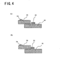
- the IC chips 32 are subsequently mounted along the head chips 20 as shown in Fig. 3(b).
- the mounting positions for the IC chips 32 are not specifically limited. As shown in Fig. 4(a), the IC chips 32 may be mounted separately from the head chips 20, and as shown in Figs. 4(b), the IC chips 32 may be mounted to closely contact the head chips 20. In the case of Fig. 4 (a), the IC chips 32 can be mounted easily, whereas in the case of Fig. 4(b), the bonding wires 34 described above can be shortened, and the entire thermal head can be made compact.
- the IC chips 32 and respective terminals are connected together through the bonding wires 34 .
- the IC chip 32 and the bonding wire 34 are molded with the sealing resin 35.
- the wiring substrate forming plate 41 is cut at predetermined locations (along broken lines 44a and 44b in Fig. 2) to form the thermal heads 10.
- the wire bonding, sealing, and cutting steps can be executed using a well known technique.
- a cutting method a method using a rotary blade, a method using a depressingly cutting, a punching method using a die set, a cutting using a router, a cutting using a laser processing, a cutting using a water jet or the like can be used.
- the mounting process as described above is high in productivity and reduces the cost remarkably since the mounting process can be executed in a state that miniature head chips 20 are joined onto the wiring substrate forming plate 41.
- the head chip 20 can be held stably using the elongated holes 42 as described above, and the cutting subsequent to the mounting can be conducted easily.
- the protruded amount H of the head chip 20 from the wiring substrate 30 of Fig. 1 is 20% or more, preferably 50% or more, of the width of the head chip 20, it is essential to hold the head chip to extend over the elongated holes as described above.
- the protruded amount exceeds 70%, there arises a problem in that the joining strength to the wiring substrate 30 is insufficient.
- the reverse side of the heating element forming portions of the head chip 20 is brought into direct contact with a heat radiating plate as described later, and accordingly, the head performance can be improved.
- a method of arraying the head chips onto the wiring substrate forming plate is also not limited, and a plate having no elongated hole may be used.
- the head chips 20 may be oriented in the same direction and arrayed into a matrix shape, or as shown in Fig. 5(b), the head chips 20 oriented in the perpendicular direction may be arrayed in a clearance between adjacent rows in which the head chips 20 are arrayed in the same direction.
- a method of forming the elongated holes is not particularly limited.
- a plurality of head chips 20 may be arrayed on the same one elongated hole 42A.
- the positioning when the head chips 20 are disposed can be made easy, and this method can cope with the head chips having different lengths.
- the thermal head 10 described above is used such that it is held on a support member that is made of a metal such as aluminum and that has a function of a heat radiating plate to form a thermal head unit.
- An example of the thermal head unit is shown in Fig. 7(a).
- a support member 50 includes an upper step portion 51 serving as a head chip supporting portion which is closely contacted with the reverse side of the end portion of the head chip 20 which is protruded from the wiring substrate 30 and which is provided with the heating elements 24 (hereafter, the end portion being referred to as the heating element forming portion when applicable), and a step difference portion 52 recessed more deeply than the thickness of the wiring substrate 30.
- the heating element forming portion i.e. the protruded portion of the head chip 20
- the heating element forming portion i.e. the protruded portion of the head chip 20
- a bottom portion of the step difference portion 52 is provided with an adhesive agent layer 54.
- the thermal head 10 is joined by the adhesive layer 53 using as a reference a contact between the reverse surface of the heating element forming portion of the head chip 20 and the upper step portion 51, and then the adhesive agent layer 54 is subjected to the hardening process (heat application, leaving under ambient temperature, irradiation of ultraviolet rays, etc.).
- the adhesive agent layer 54 is subjected to the hardening process (heat application, leaving under ambient temperature, irradiation of ultraviolet rays, etc.).
- the adhesive agent layer 54 an adhesive agent relatively soft when it is unhardened, and this makes it possible to easily realize a thermal head unit structure using, as a reference, a joining surface between the support member 50 and the head chip 20. That is, if, before the adhesive agent layer 54 on the step difference portion 52 is hardened, the heating element forming portion of the head chip 20 and the upper step portion 51 of the support member 50 are joined to each other, and the wiring substrate 30 is placed on the adhesive agent layer 54 within the step difference portion 52, and further if the adhesive agent layer 54 filled in a clearance between the wiring substrate 30 and the step difference portion 52 is a relatively soft material having a flowability or is in the form of a paste, then, even in the case where the clearance is not uniform, a joining surface between the head chip 20 and the upper step portion 51 is not adversely affected, and the joining surface between the head chip 20 and the upper step portion 51 serves as a reference surface.
- the warp of the wiring substrate 30 is absorbed by the adhesive agent layer 54 so that the heating element forming portion of the head chip 20 and the wiring substrate are closely fixed to the support member 50.
- the adhesive agent used as the adhesive agent layer 54 preferably has a flowability or a characteristic having a paste like or soft tacky property when it is unhardened. It is effective to provide the adhesive agent layer 54 thicker than the adhesive layer 53.
- the heating element forming portion i.e. the portion protruded from the wiring substrate 30
- the excess heat of the heating elements can not be escaped through the support member 50 to adversely affect the printing function. This adverse affect can be eliminated by adopting the support structure described above.
- the thermal head aimed at reducing the cost generally employs the GE substrate as the wiring substrate, and in this case also, by adopting the structure described above, it is possible to relieve the stress at the adhering boundary portion caused due to a difference in thermal expansion coefficient, to absorb the warp of the GE substrate due to the hardening process, and thus to provide the sufficient joining strength as well as to eliminate the difficult in assembly.
- the support member 50 described above is not specifically limited as far as it includes the step difference portion 52 having a depth T2 (T2 > T1) where the thickness of the wiring substrate 30 is denoted by T1.
- the step difference portion 52 is preferably in the form of a recessed portion for the purpose of preventing the flowing-out of the adhesive agent layer 54 and stably fixing connectingwirings between the circuit formed on the wiring substrate 30 and an unillustrated external driver circuit, but, for example, may be formed as a step difference portion 52A in the form of an L-shape in section as shown in Fig. 7(b).
- a groove 55 may be provided to the bottom portion of the step difference portion 52 to form a relief portion for the adhesive agent layer 54, thereby further preventing the adhesive agent layer 54 from flowing out to the surface of the support member 50.
- the groove portion 55 is not limited in number, shape, etc, and as shown in Fig. 8 (a) one groove 55 may be provided, and alternatively, two or more grooves 55 may be provided. Further, the groove 55 may be rectangular in section, or otherwise may be semicircular in section.
- the adhesive layer 53 for joining the head chip 20 to the upper step portion 51 of the support member 50 is not limited as far as it can securely establish a closely contacting state for releasing the excess heat of the heating element forming portion, and a double coated tape, a tacky agent, or an adhesive agent can be used to form the adhesive layer 53.
- a method of providing the adhesive agent layer 54 to the bottom portionof the step difference portion 52 is not specifically limited.
- a printing using a metal mask having a durability and which is effective with respect to a step difference is preferable, but an injection method using a dispenser may be adopted.
- Another material such as a sheet-like tacky agent may be used as far as it can absorbs the warp of the GE substrate and the difference in thermal expansion coefficient.
- a method of mounting the thermal head 10 to the support member 50 is not specifically limited.
- the support member 50 is set onto a jig, and the thermal head 10 is placed on the support member 50 to match with each other while using the heating element forming portion of the head chip 20 as a reference. It is also applicable to respectively add positioning marks to the support member 50 and the thermal head 10, to execute recognition and positioning using the positioning marks and to thereby place the thermal head onto the support member 50.
- the heating element forming portion of the head chip 20 and the wiring substrate 30 are simultaneously depressed onto the support member 50 to be securely contacted therewith, the hardening process for hardening the adhesive agent layer 54 is executed.
- an adhesive agent can be allowed to flow into a clearance between the wiring substrate 30 and the step difference portion 52 of the support member 50, and then the process for hardening the adhesive agent can be executed to closely contacting and fixing the thermal head 10 onto the support member 50.
- each of the IC chips 32 can be located at a relatively lower position in comparison to the structure of the background art. Therefore, the height of the sealing resin 35 can be reduced.
- This provides an advantage in that, when the head is actually mounted to a thermal printer or the like, it is possible to readily secure a conveying space for a printed sheet. That is, as shown in Fig. 9, a clearance between a platen roller 57 disposed opposite to the heating elements 24 and the sealing resin 35 can be enlarged to avoid the interference between the printed sheet 58 and the sealing resin 35.
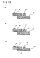
- the IC chip 32 having a height smaller than a thickness of the head chip 20, but the invention should not be limited thereto, and the similar effect can be obtained if the height of the IC chip 32 is substantially as large as the thickness of the head chip 20.
- the IC chip 32A having a height substantially as large as the thickness of the head chip 20 may be used, and as shown in Fig. 10(b), a base portion 36 may be provided below the IC chip 32 so that the height of the IC chip 32 is as large as the thickness of the head chip 20, and further, as shown in Fig. 10(c), using a wiring substrate 30A having a step difference portion 37 relatively thinner in a joining portion to the head chip 20, the height of the IC chip 32 may be as large as the thickness of the head chip 20. If the thickness of the head chip 20 is set to be substantially the same as the height of the IC chip 32 as described above, the wire bonding process can be facilitated.
- the joining state between the head chip 20 and the wiring substrate 30 is not specifically limited. As shown in Fig. 11(a), even in the case where the head chip 20 is protruded from the wiring substrate 30 as in the embodiments described above, the portion where the heating elements are provided may not be protruded entirely, and as shown in Fig. 11(b), the end face of the head chip 20 may be flush with the end face of the wiring substrate 30, and further as shown in Fig. 11(c), the end face of the head chip 20 may be located inwardly of the end face of the wiring substrate 30. Either of these cases is disadvantageous in view of releasing the head of the heating element forming portion, but advantageous in that the mounting is stable, and the head is made as compact as possible.
- the case where the end face of the head chip 20 is retracted from the end face of the wiring substrate 30 as shown in Fig. 11(c) is advantageous in that the end portion of the head chip 20 is prevented from being damaged due to contact or the like.
- the wiring substrate forming plate 41 onto which the head chips 20 are mounted may not be formed with the elongated holes 42 as mentioned above, but it is preferable to form the elongated holes 42 for the purpose of facilitating the cutting process.
- a positional relationship between the elongated hole 42 and the head chip 20 when the head chip 20 is mounted is not specifically limited. As shown in Fig. 12 (a), the end face of the head chip 20 may be confronted with the interior of the elongated hole 42, as shown in Fig. 12 (b), the end face of the head chip 20 may be flush with the inner peripheral surface of the elongated hole 42, and further as shown in Fig. 12(c), the end face of the head chip 20 may be separated from the elongated hole 42. In this case, the head chip 20 can be stably mounted, and the mounting without mutual inclination can be readily realized.
- the common electrode 27 is connected, for example, at both end portions thereof through common electrode wirings provided on the wiring substrate 30 to external terminals and then grounded.
- the electric resistance possessed by the common electrode 27 causes variation in the value of current flowing through the respective heating elements 24. That is, the value of current flowing through the heating element 24 connected to a central portion remote from the grounded portion of the common electrode 27 is small to make the generated heat amount small, thereby causing variation in print density.
- the thermal head according to the present embodiment uses the common electrode 27 the width of which is suppressed to the minimal level in order to make the width of the ceramic substrate 21 the smallest, as well as improving the connection of the common electrode 27 to the external terminals in order to eliminate the variations in print density among the respective heating elements 24.
- Fig. 13 (a) is a sectional view of a wiring connecting portion between the common electrode 27 of the head chip 20 and the common electrode wirings of the wiring substrate 30, and Fig. 13(b) is a plane view thereof.
- the wiring substrate 30 is provided with the common electrode wirings 61 so that the common electrode wirings 61 extend to the area between the adjacent IC chips 32, and these common electrode wirings 61 and the common electrode 27 provided to the end portion of the ceramic substrate 21 are connected through the bonding wires 63, respectively.
- Each of the common electrode wirings 61 is grounded through an unillustrated external terminal. That is, in the present embodiment, the common electrode 27 is connected to the common electrode wiring 61 at each of physical blocks defined by the respective IC chips 32.
- connection between the common electrode 27 and the common electrode wiring 61 of the wiring substrate 30 is provided at each of the physical blocks defined by the respective IC chips 32, it is possible to reduce the variation in print density caused due to the electric resistance of the common electrode 27. That is, it is possible to reduce the variation in the value of current flowing through the heating elements, to thereby make uniform the quantity of the heat generated from the heating elements.
- the number of the common electrode wirings 61 can be determined based on the electric resistance of the common electrode 27, the voltage applied during printing, the number of the heating elements connected to the IC chip 32, the electric resistance of the heating element, or the like.
- each of the common electrode wirings 32 may be provided for two of the IC chips 32, or a multiple, i.e. three or more, IC chips 32.
- the plural connections between the common electrode 27 of the ceramic substrate 21 and the common electrode wirings 61 of the wiring substrate 30 are provided within each physical block. That is, in the present embodiment, as shown in Fig. 15, further provided are a common electrode wiring 61A on the surface of substantially the central portion of the IC chip 32, and a common electrode wiring 61B associated therewith, and bonding wires 63A and 63B respectively connecting the common electrode 27 to the common electrode wiring 61A and the common electrode wiring 61A to the common electrode wiring 61B. Other arrangements are the same as those of the embodiments described above. In addition to the connection between the common electrode 27 and the IC chip 32, the connection is provided at the substantially longitudinal central portion of the IC chip 32 between the common electrode 27 and the common electrode wiring 61A. This makes it possible to further suppress the non-uniformity of the value of current flowing through the heating elements, thereby further reducing variation in print density.
- the number of common electrode connections provided within eachphysicalblock, the location of each connection, and a connecting manner are not specifically limited. The same effect can be obtained if a plurality of connections are provided within each physical block.
- connection within each physical block may be carried out using a common electrode wiring 61C provided below the IC chip 32 and a bonding wire 63C in place of using the common electrode wiring 61A provided on the surface of the IC chip 32.
- a bonding wire 63C in place of using the common electrode wiring 61A provided on the surface of the IC chip 32.
- a common electrode wiring 61D provided opposite from the common electrode 27 with respect to the IC chip 32 may be connected to the common electrode 27 through a bonding wire 63D extending across the IC chip 32. This case is advantageous in that a processing for providing the common electrode wiring on the IC chip 32 or the like is unnecessary.
- connection between the common electrode and the common electrode wiring is carried out using the wire bonding, but of course, the present invention is not limited thereto.
- the connection is not specifically limited as far as it can establish the electrical connection.
- Figs. 18 (a) and 18 (b) are a sectional view and a plane view of a wiring connecting portion between the head chip and the wiring substrate in a thermal head according to another embodiment.
- the height of the head chip 20 is substantially the same as the height of the wiring substrate 30, and a semiconductor integrated circuit 32B of a flip tip type are mounted onto and across the head chip 20 and the wiring substrate 30.
- the terminal portion 62 on the segment electrode 25a connected to the heating element is connected to the external terminal 33A through a pad 71 and a bump 72 provided on the lower surface of the IC chip 32B.
- the IC chip 32B is provided with pads 73 short-circuited to each other for common electrode wirings, and these pads 73 are respectively connected through bumps 74 to the common electrode 27 and the common electrode wiring 61E on the wiring substrate 30.
- the use of the IC chip 32B of the flip tip type in this manner can dispense with the connection by the wire bonding.
- wire bonding may be used for connection between the common electrode and the common electrode wiring within the IC chip of the flip tip type.
- the common electrode of the head chip is connected to the external terminal at plural locations in the direction in which the heating elements are arrayed, it is possible to reduce the print variation while suppressing the configuration of the thermal head to be small.
- the present invention it is possible to make the head chip compact in size, enhance the productivity of the board forming process, improve the handling ability during the mounting process, and remarkably reduce the cost.
Landscapes
- Engineering & Computer Science (AREA)
- Manufacturing & Machinery (AREA)
- Electronic Switches (AREA)
Claims (6)
- Thermökopfeinheit, umfassend einen Thermokopf (10), der an einem Stützelement (50) montiert ist, wobei der Thermokopf (10) einen Kopfchip (20) umfasst, mit einer Oberfläche, auf der Heizelemente (24) und Elektroden (25), die an die Heizelemente (24) angeschlossen sind, bereitgestellt sind, sowie ein Verdrahtungssubstrat (30), das mit der anderen Oberfläche des Kopfchips (20) verbunden ist, und eine integrierte Halbleiterschaltung (32), die an die Elektroden (25) angeschlossen ist, wobei die integrierte Halbleiterschaltung (32) an dem Verdrahtungssubstrat (30) montiert ist, und wobei ein Endabschnitt des Kopfchips (20), der als Heizelementbildungsabschnitt dient, von dem Verdrahtungssubstrat (30) vorragt, wobei das Stützelement (50) mit einem oberen Stufenabschnitt (51), mit dem der Heizelementbildungsabschnitt verbunden ist, und einem Stufendifferenzabschnitt (52) gebildet ist, wobei die Thermokopfeinheit dadurch gekennzeichnet ist, dass der Stufendifferenzabschnitt (52) zu dem oberen Stufenabschnitt eine tiefere Aussparung als eine Dicke des Verdrahtungssubstrats (30) hat, und eine Haftmittelschicht (54) in einem Zwischenraum bereitgestellt ist, der zwischen dem Stufendifferenzabschnitt (52) und dem Verdrahtungssubstrat (30) gebildet ist, wenn der Heizelementbildungsabschnitt des Kopfchips mit dem oberen Stufenabschnitt (51) verbunden wird.
- Thermokopfeinheit nach Anspruch 1, dadurch gekennzeichnet, dass eine Haftschicht (53) zum Verbinden des Heizelementbildungsabschnitts des Kopfchips (20) mit dem oberen Stufenabschnitt (51) bereitgestellt ist.
- Thermokopfeinheit nach Anspruch 1 oder 2, dadurch gekennzeichnet, dass eine Haftschicht (53) zum Verbinden des Heizelementbildungsabschnitts des Kopfchips (20) mit dem oberen Stufenabschnitt (51) bereitgestellt ist, und die Haftmittelschicht (54) dicker als die Haftschicht (53) ist.
- Thermokopfeinheit nach einem der Ansprüche 1 bis 3, des Weiteren dadurch gekennzeichnet, dass mindestens eine vertiefte Nut (55) an einem Boderiabschnitt des Stufendifferenzabschnitts (52) bereitgestellt ist.
- Verfahren zur Herstellung einer Thermokopfeinheit, die so konstruiert ist, dass ein Thermokopf (10) an einem Stützelement (50) gehalten wird, wobei der Thermokopf (10) einen Kopfchip (20) umfasst, mit einer oberfläche, auf der Heizelemente (24) und Elektroden (25), die an die Heizelemente (24) angeschlossen sind, bereitgestellt sind, sowie ein Verdrahtungssubstrat (30), das mit der anderen Oberfläche des Kopfchips in einem Zustand (20) verbunden ist, dass ein Endabschnitt des Kopfchips (20), der als Heizelementbildungsabschnitt dient, von dem Verdrahtungssubstrat vorragt, und auf dem eine integrierte Halbleiterschaltung (32) montiert ist, die an die Elektroden (25) angeschlossen ist, wobei das Herstellungsverfahren für die Thermokopfeinheit dadurch gekennzeichnet ist, dass es Folgendes umfasst:einen Schritt zum Aufbringen einer Haftmittelschicht (54) an einem Stufendifferenzabschnitt (52) des Stützelements (50), wobei das Stützelement (50) einen oberen Stufenabschnitt (51) aufweist, der mit dem Heizelementbildungsabsclinitt verbunden ist, und der Stufendifferenzabschnitt (52) zu dem oberen Stufenabschnitt eine tiefere Aussparung als eine Dicke (T1) des Verdrahtungssubstrats (30) hat;einen Schritt zum Anordnen des Verdrahtungssubstrats (30) auf der Haftmittelschicht (54), die an dem Stufendifferenzabschnitt (52) bereitgestellt ist, unter Verwendung einer Verbindung des Heizelementbildungsabschnitts mit dem oberen Stufenabschnitt (51) als Referenz, vor dem Härten der Haftmittelschicht (54); undeinen Schritt zum anschließenden Härten der Haftmittelschicht (54).
- Verfahren zur Herstellung einer Thermokopfeinheit, die so konstruiert ist, dass ein Thermokopf (10) an einem Stützelement (50) gehalten wird, wobei der Thermokopf (10) einen Kopfchip (20) umfasst, mit einer Oberfläche, auf der Heizelemente (24) und Elektroden (25), die an die Heizelemente (24) angeschlossen sind, bereitgestellt sind, sowie ein Verdrahtungssubstrat (30), das mit der anderen Oberfläche des Kopfchips in einem Zustand (20) verbunden ist, dass ein Endabschnitt des Kopfchips (20); der als Heizelementbildungsabschnitt dient, von dem Verdrahtungssubstrat vorragt, und auf dem eine integrierte Halbleiterschaltung (32) montiert ist, die an die Elektroden (25) angeschlossen ist, wobei das Herstellungsverfahren für die Thermokopfeinheit dadurch gekennzeichnet ist, dass es Folgendes umfasst:einen Schritt zum Bereitstellen eines Stützelements (50) mit einem oberen Stufenabschnitt (51), der mit dem Heizelementbildüngsabschnitt verbunden ist, und einem Stufendifferenzabschnitt (52), der zu dem oberen Stufenabschnitt eine tiefere Aussparung als eine Dicke (T1) des Verdrahtungssubstrats (30) hat, und zum Befestigen des Verdrahtungssubstrats (30) an dem Stufendifferenzabschnitt (52) unter Verwendung einer Verbindung des Heizelementbildungsabschnitts mit dem oberen Stufenabschnitt (51) als Referenz, während das Verdrahtungssubstrat (30) an dem Stufendifferenzabschnitt (52) mit einem Zwischenraum dazwischen angeordnet wird;einen Schritt zum Aufbringen eines Haftmittels (54) in dem Zwischenraum; undeinen Schritt zum anschließenden Härten der Haftmittelschicht (54).
Priority Applications (1)
| Application Number | Priority Date | Filing Date | Title |
|---|---|---|---|
| EP05076703A EP1602494B1 (de) | 1998-08-11 | 1999-08-09 | Verfahren zur Herstellung eines Thermokopfes |
Applications Claiming Priority (5)
| Application Number | Priority Date | Filing Date | Title |
|---|---|---|---|
| JP22710498 | 1998-08-11 | ||
| JP22710498 | 1998-08-11 | ||
| JP23460298 | 1998-08-20 | ||
| JP23460298 | 1998-08-20 | ||
| PCT/JP1999/004319 WO2000009341A1 (en) | 1998-08-11 | 1999-08-09 | Thermal head, thermal head unit, and method of manufacture thereof |
Related Child Applications (1)
| Application Number | Title | Priority Date | Filing Date |
|---|---|---|---|
| EP05076703A Division EP1602494B1 (de) | 1998-08-11 | 1999-08-09 | Verfahren zur Herstellung eines Thermokopfes |
Publications (3)
| Publication Number | Publication Date |
|---|---|
| EP1108552A1 EP1108552A1 (de) | 2001-06-20 |
| EP1108552A4 EP1108552A4 (de) | 2001-10-17 |
| EP1108552B1 true EP1108552B1 (de) | 2006-04-19 |
Family
ID=26527511
Family Applications (2)
| Application Number | Title | Priority Date | Filing Date |
|---|---|---|---|
| EP05076703A Expired - Lifetime EP1602494B1 (de) | 1998-08-11 | 1999-08-09 | Verfahren zur Herstellung eines Thermokopfes |
| EP99937006A Expired - Lifetime EP1108552B1 (de) | 1998-08-11 | 1999-08-09 | Thermokopf, thermokopfeinheit und herstellungsverfahren dafür |
Family Applications Before (1)
| Application Number | Title | Priority Date | Filing Date |
|---|---|---|---|
| EP05076703A Expired - Lifetime EP1602494B1 (de) | 1998-08-11 | 1999-08-09 | Verfahren zur Herstellung eines Thermokopfes |
Country Status (8)
| Country | Link |
|---|---|
| US (1) | US6686945B1 (de) |
| EP (2) | EP1602494B1 (de) |
| JP (1) | JP3905311B2 (de) |
| KR (1) | KR100574810B1 (de) |
| CN (1) | CN1142858C (de) |
| DE (2) | DE69941017D1 (de) |
| HK (1) | HK1041852B (de) |
| WO (1) | WO2000009341A1 (de) |
Families Citing this family (7)
| Publication number | Priority date | Publication date | Assignee | Title |
|---|---|---|---|---|
| JP2002370396A (ja) * | 2001-06-13 | 2002-12-24 | Sii P & S Inc | サーマルヘッドユニット及びその製造方法 |
| JP4939184B2 (ja) * | 2005-12-15 | 2012-05-23 | キヤノン株式会社 | 液体吐出ヘッドの製造方法 |
| CN102470677B (zh) * | 2009-08-27 | 2014-10-15 | 京瓷株式会社 | 记录头及具有该记录头的记录装置 |
| JP5943414B2 (ja) * | 2011-12-01 | 2016-07-05 | セイコーインスツル株式会社 | サーマルヘッドの製造方法 |
| JP6352799B2 (ja) * | 2014-12-24 | 2018-07-04 | 京セラ株式会社 | サーマルヘッドおよびサーマルプリンタ |
| JP6059412B1 (ja) * | 2015-03-27 | 2017-01-11 | 京セラ株式会社 | サーマルヘッドおよびサーマルプリンタ |
| US9950511B2 (en) * | 2016-02-12 | 2018-04-24 | Stmicroelectronics, Inc. | Microfluidic assembly and methods of forming same |
Family Cites Families (9)
| Publication number | Priority date | Publication date | Assignee | Title |
|---|---|---|---|---|
| JPS60117152A (ja) * | 1983-11-30 | 1985-06-24 | Toshiba Corp | 検査装置 |
| JPS60117152U (ja) * | 1984-01-17 | 1985-08-08 | ロ−ム株式会社 | 熱印字ヘツド |
| JPS63179764A (ja) * | 1987-01-22 | 1988-07-23 | Konica Corp | 感熱記録ヘツド |
| JPS63251256A (ja) * | 1987-04-08 | 1988-10-18 | Tdk Corp | サ−マルヘツド |
| US5220354A (en) * | 1990-12-18 | 1993-06-15 | Graphtec Kabushiki Kaisha | Thermal printing head |
| JPH04338556A (ja) * | 1991-05-15 | 1992-11-25 | Rohm Co Ltd | サーマルプリントヘッド |
| JPH059941U (ja) * | 1991-07-18 | 1993-02-09 | アオイ電子株式会社 | サーマルプリントヘツド |
| JP3115453B2 (ja) * | 1992-12-28 | 2000-12-04 | 三菱電機株式会社 | サーマルヘッドおよび感熱記録装置 |
| FR2730666B1 (fr) * | 1995-02-22 | 1997-04-25 | Axiohm | Tete d'imprimante thermique a plaquette support etroite |
-
1999
- 1999-08-09 CN CNB998120022A patent/CN1142858C/zh not_active Expired - Fee Related
- 1999-08-09 EP EP05076703A patent/EP1602494B1/de not_active Expired - Lifetime
- 1999-08-09 US US09/762,558 patent/US6686945B1/en not_active Expired - Fee Related
- 1999-08-09 DE DE69941017T patent/DE69941017D1/de not_active Expired - Lifetime
- 1999-08-09 JP JP2000564820A patent/JP3905311B2/ja not_active Expired - Lifetime
- 1999-08-09 HK HK02103593.3A patent/HK1041852B/zh not_active IP Right Cessation
- 1999-08-09 WO PCT/JP1999/004319 patent/WO2000009341A1/ja not_active Ceased
- 1999-08-09 KR KR1020017001752A patent/KR100574810B1/ko not_active Expired - Fee Related
- 1999-08-09 EP EP99937006A patent/EP1108552B1/de not_active Expired - Lifetime
- 1999-08-09 DE DE69930946T patent/DE69930946T2/de not_active Expired - Lifetime
Also Published As
| Publication number | Publication date |
|---|---|
| CN1142858C (zh) | 2004-03-24 |
| DE69930946D1 (de) | 2006-05-24 |
| DE69941017D1 (de) | 2009-07-30 |
| HK1041852B (zh) | 2005-01-21 |
| KR100574810B1 (ko) | 2006-04-27 |
| KR20010074815A (ko) | 2001-08-09 |
| CN1323263A (zh) | 2001-11-21 |
| US6686945B1 (en) | 2004-02-03 |
| EP1108552A4 (de) | 2001-10-17 |
| HK1041852A1 (en) | 2002-07-26 |
| JP3905311B2 (ja) | 2007-04-18 |
| DE69930946T2 (de) | 2006-09-07 |
| EP1108552A1 (de) | 2001-06-20 |
| EP1602494A3 (de) | 2006-11-08 |
| WO2000009341A1 (en) | 2000-02-24 |
| EP1602494A2 (de) | 2005-12-07 |
| EP1602494B1 (de) | 2009-06-17 |
Similar Documents
| Publication | Publication Date | Title |
|---|---|---|
| US20070126798A1 (en) | Ink jet recording head and manufacturing method thereof | |
| EP1108552B1 (de) | Thermokopf, thermokopfeinheit und herstellungsverfahren dafür | |
| US7115975B2 (en) | Semiconductor device, process of producing semiconductor device, and ink jet recording head | |
| JP4549171B2 (ja) | 混成集積回路装置 | |
| US7789488B2 (en) | Flexible wiring board and liquid discharge head | |
| EP1582360B1 (de) | Thermokopf mit zwischen Kühlkörperplatte und Kopfsubstrat aufgetragenem Klebstof und Herstellungsverfahren dafür | |
| US5870128A (en) | Light-emitting device assembly having in-line light-emitting device arrays and manufacturing method therefor | |
| US6606109B1 (en) | Thermal head and thermal head unit | |
| US7159969B2 (en) | Composite ink jet printhead and relative manufacturing process | |
| US7571993B2 (en) | Ink-jet head | |
| JPS63179764A (ja) | 感熱記録ヘツド | |
| JPWO2000009341A1 (ja) | サーマルヘッド及びサーマルヘッドユニット並びにその製造方法 | |
| JPS6221559A (ja) | サ−マルヘツド | |
| JP4068647B2 (ja) | サーマルヘッドの製造方法 | |
| JPH05254164A (ja) | 高密度実装機能デバイス | |
| JP3362234B2 (ja) | 電子部品およびその製造方法 | |
| JPH0243059A (ja) | プリンタヘッドの電子部品保護構造 | |
| JPH0632932B2 (ja) | サーマルヘッドの製造方法 | |
| JP3017157B2 (ja) | サーマルプリントヘッドの構造 | |
| JPH01258961A (ja) | 集積回路装置の製造方法及び集積回路装置用基板 | |
| JP2023153472A (ja) | サーマルプリントヘッドの製造方法、およびサーマルプリントヘッド | |
| JPH11151814A (ja) | インクジェットヘッドおよびインクジェットヘッドの組立方法 | |
| JP2001160603A (ja) | 半導体装置およびその製造方法 | |
| JPS62156973A (ja) | 電子装置 | |
| JPH08290600A (ja) | サーマルヘッド |
Legal Events
| Date | Code | Title | Description |
|---|---|---|---|
| PUAI | Public reference made under article 153(3) epc to a published international application that has entered the european phase |
Free format text: ORIGINAL CODE: 0009012 |
|
| 17P | Request for examination filed |
Effective date: 20010219 |
|
| AK | Designated contracting states |
Kind code of ref document: A1 Designated state(s): AT BE CH CY DE DK ES FI FR GB GR IE IT LI LU MC NL PT SE |
|
| RIC1 | Information provided on ipc code assigned before grant |
Free format text: 7B 41J 2/345 A |
|
| A4 | Supplementary search report drawn up and despatched |
Effective date: 20010905 |
|
| AK | Designated contracting states |
Kind code of ref document: A4 Designated state(s): AT BE CH CY DE DK ES FI FR GB GR IE IT LI LU MC NL PT SE |
|
| RBV | Designated contracting states (corrected) |
Designated state(s): DE IT |
|
| 17Q | First examination report despatched |
Effective date: 20041203 |
|
| GRAP | Despatch of communication of intention to grant a patent |
Free format text: ORIGINAL CODE: EPIDOSNIGR1 |
|
| GRAS | Grant fee paid |
Free format text: ORIGINAL CODE: EPIDOSNIGR3 |
|
| GRAA | (expected) grant |
Free format text: ORIGINAL CODE: 0009210 |
|
| AK | Designated contracting states |
Kind code of ref document: B1 Designated state(s): DE IT |
|
| REF | Corresponds to: |
Ref document number: 69930946 Country of ref document: DE Date of ref document: 20060524 Kind code of ref document: P |
|
| PLBE | No opposition filed within time limit |
Free format text: ORIGINAL CODE: 0009261 |
|
| STAA | Information on the status of an ep patent application or granted ep patent |
Free format text: STATUS: NO OPPOSITION FILED WITHIN TIME LIMIT |
|
| 26N | No opposition filed |
Effective date: 20070122 |
|
| PGFP | Annual fee paid to national office [announced via postgrant information from national office to epo] |
Ref country code: DE Payment date: 20110803 Year of fee payment: 13 |
|
| PGFP | Annual fee paid to national office [announced via postgrant information from national office to epo] |
Ref country code: IT Payment date: 20110811 Year of fee payment: 13 |
|
| PG25 | Lapsed in a contracting state [announced via postgrant information from national office to epo] |
Ref country code: IT Free format text: LAPSE BECAUSE OF NON-PAYMENT OF DUE FEES Effective date: 20120809 |
|
| PG25 | Lapsed in a contracting state [announced via postgrant information from national office to epo] |
Ref country code: DE Free format text: LAPSE BECAUSE OF NON-PAYMENT OF DUE FEES Effective date: 20130301 |
|
| REG | Reference to a national code |
Ref country code: DE Ref legal event code: R119 Ref document number: 69930946 Country of ref document: DE Effective date: 20130301 |