EP1102234A2 - Active matrix type display apparatus and drive circuit thereof - Google Patents
Active matrix type display apparatus and drive circuit thereof Download PDFInfo
- Publication number
- EP1102234A2 EP1102234A2 EP00310214A EP00310214A EP1102234A2 EP 1102234 A2 EP1102234 A2 EP 1102234A2 EP 00310214 A EP00310214 A EP 00310214A EP 00310214 A EP00310214 A EP 00310214A EP 1102234 A2 EP1102234 A2 EP 1102234A2
- Authority
- EP
- European Patent Office
- Prior art keywords
- thin film
- drive
- field effect
- type field
- effect transistor
- Prior art date
- Legal status (The legal status is an assumption and is not a legal conclusion. Google has not performed a legal analysis and makes no representation as to the accuracy of the status listed.)
- Withdrawn
Links
Images

Classifications
-
- G—PHYSICS
- G09—EDUCATION; CRYPTOGRAPHY; DISPLAY; ADVERTISING; SEALS
- G09G—ARRANGEMENTS OR CIRCUITS FOR CONTROL OF INDICATING DEVICES USING STATIC MEANS TO PRESENT VARIABLE INFORMATION
- G09G3/00—Control arrangements or circuits, of interest only in connection with visual indicators other than cathode-ray tubes
- G09G3/20—Control arrangements or circuits, of interest only in connection with visual indicators other than cathode-ray tubes for presentation of an assembly of a number of characters, e.g. a page, by composing the assembly by combination of individual elements arranged in a matrix no fixed position being assigned to or needed to be assigned to the individual characters or partial characters
- G09G3/22—Control arrangements or circuits, of interest only in connection with visual indicators other than cathode-ray tubes for presentation of an assembly of a number of characters, e.g. a page, by composing the assembly by combination of individual elements arranged in a matrix no fixed position being assigned to or needed to be assigned to the individual characters or partial characters using controlled light sources
- G09G3/30—Control arrangements or circuits, of interest only in connection with visual indicators other than cathode-ray tubes for presentation of an assembly of a number of characters, e.g. a page, by composing the assembly by combination of individual elements arranged in a matrix no fixed position being assigned to or needed to be assigned to the individual characters or partial characters using controlled light sources using electroluminescent panels
-
- G—PHYSICS
- G09—EDUCATION; CRYPTOGRAPHY; DISPLAY; ADVERTISING; SEALS
- G09G—ARRANGEMENTS OR CIRCUITS FOR CONTROL OF INDICATING DEVICES USING STATIC MEANS TO PRESENT VARIABLE INFORMATION
- G09G3/00—Control arrangements or circuits, of interest only in connection with visual indicators other than cathode-ray tubes
- G09G3/20—Control arrangements or circuits, of interest only in connection with visual indicators other than cathode-ray tubes for presentation of an assembly of a number of characters, e.g. a page, by composing the assembly by combination of individual elements arranged in a matrix no fixed position being assigned to or needed to be assigned to the individual characters or partial characters
- G09G3/22—Control arrangements or circuits, of interest only in connection with visual indicators other than cathode-ray tubes for presentation of an assembly of a number of characters, e.g. a page, by composing the assembly by combination of individual elements arranged in a matrix no fixed position being assigned to or needed to be assigned to the individual characters or partial characters using controlled light sources
- G09G3/30—Control arrangements or circuits, of interest only in connection with visual indicators other than cathode-ray tubes for presentation of an assembly of a number of characters, e.g. a page, by composing the assembly by combination of individual elements arranged in a matrix no fixed position being assigned to or needed to be assigned to the individual characters or partial characters using controlled light sources using electroluminescent panels
- G09G3/32—Control arrangements or circuits, of interest only in connection with visual indicators other than cathode-ray tubes for presentation of an assembly of a number of characters, e.g. a page, by composing the assembly by combination of individual elements arranged in a matrix no fixed position being assigned to or needed to be assigned to the individual characters or partial characters using controlled light sources using electroluminescent panels semiconductive, e.g. using light-emitting diodes [LED]
- G09G3/3208—Control arrangements or circuits, of interest only in connection with visual indicators other than cathode-ray tubes for presentation of an assembly of a number of characters, e.g. a page, by composing the assembly by combination of individual elements arranged in a matrix no fixed position being assigned to or needed to be assigned to the individual characters or partial characters using controlled light sources using electroluminescent panels semiconductive, e.g. using light-emitting diodes [LED] organic, e.g. using organic light-emitting diodes [OLED]
- G09G3/3225—Control arrangements or circuits, of interest only in connection with visual indicators other than cathode-ray tubes for presentation of an assembly of a number of characters, e.g. a page, by composing the assembly by combination of individual elements arranged in a matrix no fixed position being assigned to or needed to be assigned to the individual characters or partial characters using controlled light sources using electroluminescent panels semiconductive, e.g. using light-emitting diodes [LED] organic, e.g. using organic light-emitting diodes [OLED] using an active matrix
- G09G3/3233—Control arrangements or circuits, of interest only in connection with visual indicators other than cathode-ray tubes for presentation of an assembly of a number of characters, e.g. a page, by composing the assembly by combination of individual elements arranged in a matrix no fixed position being assigned to or needed to be assigned to the individual characters or partial characters using controlled light sources using electroluminescent panels semiconductive, e.g. using light-emitting diodes [LED] organic, e.g. using organic light-emitting diodes [OLED] using an active matrix with pixel circuitry controlling the current through the light-emitting element
- G09G3/3241—Control arrangements or circuits, of interest only in connection with visual indicators other than cathode-ray tubes for presentation of an assembly of a number of characters, e.g. a page, by composing the assembly by combination of individual elements arranged in a matrix no fixed position being assigned to or needed to be assigned to the individual characters or partial characters using controlled light sources using electroluminescent panels semiconductive, e.g. using light-emitting diodes [LED] organic, e.g. using organic light-emitting diodes [OLED] using an active matrix with pixel circuitry controlling the current through the light-emitting element the current through the light-emitting element being set using a data current provided by the data driver, e.g. by using a two-transistor current mirror
-
- G—PHYSICS
- G09—EDUCATION; CRYPTOGRAPHY; DISPLAY; ADVERTISING; SEALS
- G09G—ARRANGEMENTS OR CIRCUITS FOR CONTROL OF INDICATING DEVICES USING STATIC MEANS TO PRESENT VARIABLE INFORMATION
- G09G2300/00—Aspects of the constitution of display devices
- G09G2300/08—Active matrix structure, i.e. with use of active elements, inclusive of non-linear two terminal elements, in the pixels together with light emitting or modulating elements
- G09G2300/0809—Several active elements per pixel in active matrix panels
- G09G2300/0842—Several active elements per pixel in active matrix panels forming a memory circuit, e.g. a dynamic memory with one capacitor
-
- G—PHYSICS
- G09—EDUCATION; CRYPTOGRAPHY; DISPLAY; ADVERTISING; SEALS
- G09G—ARRANGEMENTS OR CIRCUITS FOR CONTROL OF INDICATING DEVICES USING STATIC MEANS TO PRESENT VARIABLE INFORMATION
- G09G2310/00—Command of the display device
- G09G2310/02—Addressing, scanning or driving the display screen or processing steps related thereto
- G09G2310/0262—The addressing of the pixel, in a display other than an active matrix LCD, involving the control of two or more scan electrodes or two or more data electrodes, e.g. pixel voltage dependent on signals of two data electrodes
Definitions
- This invention relates to a display apparatus which employs a plurality of light emitting elements such as organic electro-luminescence elements that are controlled their intensity by currents flowing through each picture element.
- This invention is particularly relates to a display apparatus of so-called an active matrix type display apparatus in which amount of current supplied to each light emitting element is controlled with active elements such as insulated gate type field effect transistors equipped in each picture element.
- this invention further relates to a drive circuit to be applied to such active matrix type display apparatus, wherein leakage current of sub-threshold level flowing through the insulated gate type field effect transistors is effectively suppressed.
- a picture display apparatus of an active matrix type a plurality of picture elements are arranged in a matrix form, and a video image is displayed by controlling intensity of each picture element according to given intensity information of the video image. Transmission factor of each picture element changes according to an applied voltage to each picture element when a liquid crystal device is used as an electro-optic material. Also in the picture display apparatus of the active matrix type employing organic materials as the electro-optic materials, the operation thereof is similar to the operation of the liquid crystal device. However different from the liquid crystal display, an organic EL (Electro-Luminescence) display is so-called self-radiation type display having a light emitting device at each picture element, so that the EL display has advantages over the liquid crystal device as follows.
- a visibility of a video image is higher, a back-light is not necessary and a response speed thereof is faster than that of the liquid crystal display.
- Intensity of the individual light emitting device of the organic EL (Electro Luminescence) display is controlled by the amount of drive current. Namely, the organic EL display is greatly different from the liquid crystal display in the point that the light emitting device is a current control type or a current drive type element.
- the organic EL display can possibly take both a simple matrix type and an active matrix type as the drive system.
- the simple matrix type drive system a construction thereof is simple, but it is difficult to apply a large-scale display and a high definition display. Accordingly the development for the active matrix system is more active than for the simple matrix type system.
- the active matrix system the current flowing through the light emitting device of each picture element is controlled with an active element (Thin Film type Transistor (TFT) which is one of an insulated gate type field effect transistor) fabricated in the picture element.
- TFT Thin Film type Transistor
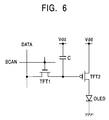
- An example of one picture element in the organic EL display of this active matrix system is depicted in Fig. 6 as an equivalent circuit.
- Each picture element comprises of a light emitting device OLED, a first thin film transistor TFT 1, a second thin film transistor TFT 2 and a retention capacitor C.
- the light emitting device is an organic electro-luminescence (EL) element.
- the most of the organic Electro-luminescence device has a rectification characteristic so that the EL element can be called as an OLED (Organic Light Emitting Diode) device, and in this Fig. 6, a sign of a diode device is applied to a sign for the light emitting device OLED.
- the light emitting device is not limited to the OLED device, and another type light emitting element can be applied if an intensity of such element is controlled by the drive current flowing through the element.
- a source electrode of the P-channel type transistor TFT 2 is connected to a Vdd (power potential)
- a cathode electrode of the light emitting device OLED is connected to ground potential
- an anode electrode of the light emitting device OLED is connected to a drain electrode of the P-channel type transistor TFT 2.
- a gate electrode of the N-channel type transistor TFT 1 is connected to a scanning line SCAN
- a source electrode thereof is connected to a data line DATA
- a drain electrode thereof is connected to both the retention capacitor C and a gate electrode of the transistor TFT 2.
- the scanning line SCAN is made in selected status in order to drive the picture element, then a data potential (signal voltage) Vw representing an intensity information is given to the data line DATA. Then the transistor TFT 1 is made ON, thereby the retention capacitor C charges or discharges and a gate potential of the transistor TFT 2 becomes to the data potential Vw. After that the scanning line SCAN is made in non-selected status, and the transistor TFT 1 is accordingly made OFF. In this case, the transistor TFT 2 is separated electrically from the data line DATA, but the gate potential of the transistor TFT 2 is maintained in stable by virtue of the retention capacitor C.
- a current flowing through the light emitting device OLED by way of the transistor TFT 2 corresponds to a value of a gate-source voltage Vgs of the transistor TFT 2, so that the light emitting device OLED continues to emit light with the intensity corresponding to the current amount supplied through the transistor TFT 2.
- a current Ids flowing between the drain-source of the transistor TFT 2 is a drive current to be supplied to the light emitting device OLED.
- the drive current Ids is shown with a following expression.
- Cox ⁇ 0 x ⁇ r/d
- the Vth shows a threshold voltage of the transistor TFT 2
- the ⁇ shows a mobility of a carrier
- the W shows a channel width
- the L shows a channel length
- the ⁇ 0 shows an electric constant
- the ⁇ r shows a relative permittivity of a gate insulator film
- the d is a thickness of the gate insulator film.
- the drive current Ids can be controlled by the data potential Vw to be applied to the picture element.
- the intensity of the light emitting device OLED can be controlled in accordance with the drive current Ids.
- the reason for operating the transistor TFT 2 in the saturation range is explained as follows. Namely the drive current Ids is controlled only by the gate-source voltage Vgs of the transistor TFT 2 in the saturation range, and the drive current Ids does not depend on the drain-source voltage Vds of the transistor TFT 2. Namely, even if the drain-source voltage Vds of the transistor TFT 2 changes by characteristic dispersion of the light emitting device OLED, a predetermined amount of the drive current Ids can be stably supplied to the light emitting device OLED.
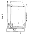
- the active matrix type display apparatus is constituted by arranging a plurality of the picture elements such as depicted in Fig. 6 in a matrix form.
- scanning lines SCAN-1 to SCAN-N for selecting one picture element 25 with a predetermined scanning cycle (one frame of the NTSC standard) and data lines DATA for giving a intensity information (the data potential Vw) to one picture element 25 are arranged in a matrix form.
- the scanning lines SCAN-1 to SCAN-N are connected to a scanning line drive circuit 21, and data lines DATA are connected to a data line drive circuit 22.
- a desired video image can be displayed by repeating the supply of the data potential Vw through the data lines DATA by the data line drive circuit 22 while selecting scanning lines SCAN-1 to SCAN-N by the scanning line drive circuit 21.
- the light emitting device emits light at the moment when selected, but in a active matrix type display apparatus as shown in Fig. 7, the light emitting device of each picture element 25 continues to emit light even after finishing the selection, thereby a total amount of the drive current can be reduced in the active matrix type display apparatus compared with the simple matrix type display apparatus and this becomes profitable with a display apparatus of, in particular, a large-sized and a high definition type.
- a TFT (Thin Film Transistor) device formed on the glass substrate is utilized as an active element, and this depends on the next reason. Namely, as the organic EL display is a direct viewing type display, the size of the display becomes comparatively large. Therefore it is not realistic to use a single crystal silicon substrate for fabricating an active element for the display due to a production cost or constraint of production facility.
- TFT Thin Film Transistor
- a comparatively large-sized glass substrate is used, and it is normal that the TFT device that it is comparatively easy to form on the glass substrate is used as an active element.
- amorphous silicon and poly-silicon used for fabricating the TFT device show bad crystallization characteristics compared with single crystal silicon and controllability of conduction mechanism is bad, so that fabricated TFT device shows relatively large dispersion of characteristic.
- a laser annealer is usually employed in order to avoid a problem of heat transformation of the glass substrate. But in this case, it is difficult to uniformly irradiate laser energy on the large-sized glass substrate, so that dispersion by the place for crystalline condition of poly-silicon is not avoided.
- the threshold voltage Vth of the TFT device for a picture element shows a dispersion of several hundreds mV, or even more than 1V among the TFT devices formed on the same substrate.
- the drive current Ids flowing through the each OLED device differs from desired value depending on the aforesaid expression (1) due to the dispersion of the threshold voltage Vth of the TFT device, so that as a result it can not be expected to obtain a a display apparatus of high picture quality at all.
- This can say about dispersion of a carrier mobility ⁇ and each parameter of the expression (1) are similar in addition to the threshold voltage Vth.
- the dispersion of each parameter as mentioned above is affected not only by the dispersion between the picture elements, but also affected by fabrication lot, every manufacturing lot or every product to some extent.
- this is not only unrealistic in mass production process of the display apparatus, but also very difficult to take measures to meet the situation for the change in characteristic drift of the TFT device by environmental temperature and change in properties with time for the TFT device produced by activity of a long term use.
- a display apparatus of the present invention comprises a scanning line drive circuit for sequentially selecting scanning lines, a data line drive circuit which contains a current source for generating signal current having current level corresponding to an intensity information and for supplying thus generated signal current sequentially to the data lines, and a plurality of picture elements each having a light emitting device of current drive type which emits light with supply of drive current, wherein the picture element is provided at each cross point of the data line and the scanning line.
- Each picture element comprises an accept section for accepting signal currents from corresponding data line when selected, a converting section for converting accepted signal current once into corresponding voltage level and restoring the voltage level and a drive section for supplying a drive current having current level corresponding to the restored voltage level to the corresponding light emitting device.
- the converting section includes the conversion thin film transistor having a gate electrode, a source electrode, a drain electrode and a channel and a capacitor connected to the gate electrode of the transistor.
- the above mentioned conversion thin film transistor generates at the gate electrode the voltage level converted by flowing through the channel the signal current taken through the accept section and the capacitor holds the voltage level generated at the gate electrode.
- the above mentioned drive section contains the drive thin film transistor including a gate electrode, a drain electrode, a source electrode and a channel and the drive thin film transistor supplies, through the channel, the drive current to the light emitting device, wherein the drive current has the current level corresponding to the voltage level stored in the capacitor and accepted at the gate electrode of the transistor.
- a threshold voltage of the drive thin film transistor is set not to become lower than a threshold voltage of the conversion thin film transistor corresponding to the picture element.
- a gate length of the drive thin film transistor is set not to be shorter than a gate length of the conversion thin film transistor.
- thickness of a gate insulator of the drive thin film transistor may be set not to be thinner than thickness of a gate insulator of the conversion thin film transistor corresponding to the picture element.
- the threshold voltage of the drive thin film transistor may be set not to be lower than the threshold voltage of the conversion thin film transistor corresponding to the picture element by adjusting impurity density injected in the channel of the drive thin film transistor.
- the drive thin film insulated gate type field effect transistor works in saturation range and supplies drive current corresponding to the difference between the threshold voltage and the voltage level given to the gate electrode into the light emitting device.
- a current mirror circuit is constituted by directly connecting the gate electrode of the drive thin film transistor to the gate electrode of the conversion thin film transistor, so that the current level of the signal current and the current level of the drive current are made to be a proportional relation.
- accept section includes the switch thin film transistor interposed between the drain electrode and the gate electrode of the conversion thin film transistor and this switch thin film transistor is made ON when the current level of the signal current is converted into the voltage level, and generates at the gate electrode of the conversion thin film transistor a voltage level referenced with the source electrode by electrically connecting the gate electrode and the drain electrode of the conversion thin film transistor.
- the organic electro-luminescence device OLED
- TFT thin film transistor
- FET drive insulated gate type field effect transistor
- conversion insulated gate type field effect transistor FET
- the hereinafter described embodiment of the invention presents a display apparatus capable of displaying a high quality image by supplying desired drive current to a light emitting device of each picture element in stable and precision in spite of characteristic dispersion of each active device of the picture element.
- the drive circuit of the invention prevents slight luminescence of the picture element by the leakage current.
- a picture element drive circuit of this invention preferably has following features. Firstly a writing of the intensity information to the picture element is done by supplying the signal current corresponding to the intensity into the data line and the signal current flows through the source-drain of the conversion insulated gate type field effect transistor in the picture element, and thereby generates a gate-source voltage corresponding to the signal current. Secondly, thus generated gate-source voltage or the gate voltage is retained in a operation of a capacitance formed in the picture element or a capacitance existing parasitically and is kept within a predetermined interval even after the completion ofthe writing of the intensity information to the picture element.
- the current flowing through the OLED device is controlled by the conversion insulated gate type field effect transistor oneself connected thereto in series or the drive insulated gate type field effect transistor which is in addition provided in the picture element and the gate electrode thereof is connected to the gate electrode of the conversion field effect transistor.
- the gate-source voltage upon driving the OLED device is approximately equal to the gate-source voltage of the conversion field effect transistor generated due to the above described first feature.
- the data line and the picture element is connected by the input insulated gate type field effect transistor which is controlled by a first scanning line and the gate-drain of the conversion insulated gate type field effect transistor is short-circuited by the switch insulated gate type field effect transistor controlled by a second scanning line.
- the intensity information is given in the form of voltage value in the conventional case, but the intensity information is given in the form of current value, namely it is current writing type in the display apparatus of the present invention.
- the conversion insulated gate type field effect transistor is called as a transistor TFT 1
- the drive insulated gate type field effect transistor is called as a transistor TFT 2
- the input insulated gate type field effect transistor is called as a transistor TFT 3
- the switch insulated gate type field effect transistor is called as a transistor TFT 4.
- these transistors are not limited to thin film transistors, and an insulated gate type field effect transistor such as a single crystal silicon transistor made on a single crystal silicon substrate or a SOI (Silicon On Insulator) substrate can broadly adopt as an active element of the present invention.
- signal current to flow in the transistor TFT 1 is defined as a signal current Iw and as a result, voltage between the gate and the source electrodes of the transistor TFT 1 is defined as a voltage Vgs.
- the transistor TFT 1 works in the saturation range because the gate and drain electrodes of the transistor TFT 1 are short-circuited by the transistor TFT 4 during writing operation.
- the Vth1 of the conversion transistor TFT 1 and the Vth2 of the drive transistor TFT 2 are basically same, so that both the transistors TFT 1 and TFT 2 are to be made OFF when a signal voltage for cutting off is supplied to respective gate of both transistors TFT 1 and TFT 2. But practically due to the dispersion of parameters in respective picture element, sometimes the Vth2 goes down below the Vth1. In this case, a leakage current corresponding to the sub-threshold level flows through the drive transistor TFT 2, so that the OLED device shows a minute luminescence. Because of this minute luminescence, contrast of the displayed image is lowered and the display characteristics are deteriorated.
- the threshold voltage Vth2 of the drive transistor TFT 2 does not become lower than the threshold voltage Vth1 of the corresponding conversion transistor TFT 1 within the picture element.
- the gate length L2 of the drive transistor TFT 2 is set to be longer than the gate length L1 of the conversion transistor TFT 1 in order to attain that the threshold voltage Vth2 of the drive transistor TFT 2 does not become lower than the threshold voltage Vth1 of the corresponding conversion transistor TFT 1.
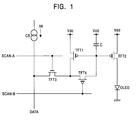
- Fig. 1 is an example of a picture element drive circuit according to the present invention.
- the picture element drive circuit includes a conversion thin film transistor TFT 1, where the signal current flows through the transistor TFT 1, and a drive thin film transistor TFT 2 for controlling the drive current flowing through a light emitting device consisting of an organic electro-luminescence device.
- the picture element drive circuit further includes an input thin film transistor TFT 3 for connecting and disconnecting the picture element drive circuit to/from a data line DATA consisting of Mo-Ta in accordance with a control signal supplied from a first scan line SCAN-A consisting of A1, a switch thin film transistor TFT 4 for connecting a gate electrode and a drain electrode of the conversion transistor TFT 1 in accordance with a control signal supplied from a second scan line SCAN-B consisting of Mo-Ta during writing period, a capacitor C having a structure the same as a metal oxide semiconductor structure of the TFT 1 for maintaining a gate-source voltage of the conversion transistor TFT 1 after completion of the writing period and a light emitting device OLED (Organic Light Emitting Device).
- OLED Organic Light Emitting Device
- the input transistor TFT 3 is an NMOS (N-channel Metal Oxide semiconductor) transistor and the other transistors are PMOS (P-channel Metal Oxide Semiconductor) transistors, but those are not limitation of a scope of the invention.
- the capacitor C one of terminals is connected to a gate electrode of the conversion transistor TFT 1 and the other terminal is connected to a potential Vdd (power potential), but it is not limited to the power potential Vdd and any arbitrary fixed potential is available.
- a cathode electrode of the light emitting device OLED is connected to ground potential.
- the display apparatus of the present invention basically comprises a scanning line drive circuit for sequentially selecting scanning lines SCAN-A and SCAN-B, a data line drive circuit including a current source CS for generating a signal current Iw having current level corresponding to intensity information and for supplying the signal current Iw sequentially to the data line DATA and a plurality of picture elements including current drive type light emitting device OLED provided at crossing portions of each scanning lines SCAN-A, SCAN-B and each data line DATA for emitting light in accordance with the received drive current.
- a scanning line drive circuit for sequentially selecting scanning lines SCAN-A and SCAN-B
- a data line drive circuit including a current source CS for generating a signal current Iw having current level corresponding to intensity information and for supplying the signal current Iw sequentially to the data line DATA and a plurality of picture elements including current drive type light emitting device OLED provided at crossing portions of each scanning lines SCAN-A, SCAN-B and each data line DATA for emitting light in accordance with the
- the above mentioned accept section consists of the input transistor TFT 3 to be concrete.
- the converting section includes the conversion thin film transistor TFT 1 having, as above mentioned, the gate electrode, the source electrode, the drain electrode and a channel and the capacitor C connected to the gate electrode of the transistor TFT 1.
- the conversion thin film transistor TFT 1 generates at the gate electrode the voltage converted by flowing through the channel the signal current Iw taken and the capacitor C restores the voltage thus generated at the gate electrode of the transistor TFT 1.
- the above mentioned accept section includes the switch thin film transistor TFT 4 interposed between the drain electrode and the gate electrode of the conversion thin film transistor TFT 1. This switch thin film transistor TFT 4 is made ON when the current level of the signal current Iw is converted into the voltage level, and generates at the gate electrode of the conversion thin film transistor TFT 1 the voltage referenced with the source electrode by electrically connecting the gate electrode and the drain electrode of the conversion thin film transistor TFT 1.
- the switch thin film transistor TFT 4 is made OFF when restoring the voltage in the capacitor C and the transistor TFT 4 disconnects the gate electrode of the conversion thin film transistor TFT 1 and the capacitor C connected thereto from the drain electrode of the conversion thin film transistor TFT 1.
- the above mentioned drive section contains the drive thin film transistor TFT 2 including the gate electrode, the drain electrode, the source electrode and a channel.
- the drive thin film transistor TFT 2 supplies, through the channel, the drive current to the light emitting device OLED, wherein the drive current has the current level corresponding to the voltage level stored in the capacitor C and accepted at the gate electrode of the transistor TFT 2.
- a current mirror circuit is constituted by directly connecting the gate electrode of the drive thin film transistor TFT 2 to the gate electrode of the conversion thin film transistor TFT 1, so that the current level of the signal current Iw and the current level of the drive current are made to be a proportional relation.
- the drive thin film transistor TFT 2 works in the saturation range, and the transistor TFT 2 flows the drive current corresponding to the difference between the voltage level given to the gate electrode and the threshold voltage to the light emitting device OLED.
- the threshold voltage of the drive thin film transistor TFT 2 is set not to become lower than the threshold voltage of the conversion thin film transistor TFT 1 within the picture element.
- a gate length of the transistor TFT 2 is set not to be shorter than a gate length of the transistor TFT 1.
- thickness of a gate insulating film of the transistor TFT 2 may be set not to be thinner than thickness of a gate insulating film of the transistor TFT 1 corresponding to the picture element.
- the threshold voltage of the transistor TFT 2 may be set not to be lower than the threshold voltage of the transistor TFT 1 within the picture element by adjusting impurity density injected in the channel of the transistor TFT 2 in the process of fabrication.
- both the transistors TFT 1 and TFT 2 are to be made OFF when a signal voltage for cutting off is supplied to commonly connected gate electrodes of both transistors TFT 1 and TFT 2.
- the threshold voltage Vth2 of the transistor TFT 2 goes down below the threshold voltage Vth1 of the transistor TFT 1.
- a leakage current corresponding to a sub-threshold level flows through the drive transistor TFT 2 even by the signal voltage of below the cut off level, so that the OLED device shows a minute luminescence and contrast of the displayed image is lowered.
- the gate length L2 of the drive transistor TFT 2 is set to be longer than the gate length L1 of the conversion transistor TFT 1.
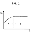
- Fig. 2 is a graph chart showing a relation between a threshold voltage Vth and a gate length L of a thin film transistor.
- the threshold voltage Vth becomes high as the gate length L increases.
- the gate length L2 of the transistor TFT 2 is made longer than the gate length L1 of the transistor TFT 1 in this invention.
- the gate length L1 of the transistor TFT 1 is set to be 7 ⁇ m, then the gate length L2 of the transistor TFT 2 is set to be about 10 ⁇ m.
- the gate length L1 of the transistor TFT 1 belongs to the short-channel effect area A, and the gate length L2 of the transistor TFT 2 belongs to the suppression area B. Thereby, not only the short channel effect in the transistor TFT 2 can be suppressed, but also it is possible to suppress Accordingly, the minute luminescence of the OLED device is restrained by suppressing the leakage current of the sub-threshold level flowing through the transistor TFT 2, thereby this can contribute to the contrast improvement of the active matrix type display apparatus. To be more concrete, when mask patterns are designed for fabrication, this idea is taken in consideration, so that the gate length L2 of the transistor TFT 2 is set to be longer than the gate length L1 of the transistor TFT 1 without requiring any extra fabrication process.
- Fig. 3 is a sectional view showing a construction of the display apparatus of this invention. Only the OLED device and the transistor TFT 2 are depicted in Fig. 3 for simplicity.
- the OLED device is formed by sequentially superimposing a reflection electrode 10 made of Mg-Ag, for example, an organic EL layer 11 and a transparent electrode 12 made of ITO (Indium Tin Oxide).
- the reflection electrode 10 is separated by one picture element and functions to be the anode electrode of the OLED device.
- Each of the transparent electrode 12 is commonly connected between the picture elements and functions to be the cathode electrode of the OLED device. Namely each of the transparent electrode 12 is commonly connected to the predetermined power potential Vdd.
- the organic EL layer 11 is a complex film formed by superimposing a positive hole transport layer and an electron transport layer. Diamyne is evaporated on the transparent electrode 10 functioning as the anode electrode (a positive hole injection electrode), Alq3 is evaporated thereon as the electron transport layer and finally the transparent electrode 12 is formed on the Alq3 functioning as the cathode electrode (an electron injection electrode).
- the above mentioned Alq3 represents an 8-hydroxy quinoline aluminum.
- the OLED device having such laminated structure is only one example and this invention is not limited by the depicted structure.
- a forward direction voltage of around 10V is supplied between the anode electrode and the cathode electrode of the OLED device having configuration as above described, injection of carriers such as the electron or the positive hole occurs and the luminescence is observed.
- the luminescent operation of the OLED device is thought to be based on an excitation formed by both the positive hole injected from the positive hole transport layer and the electron injected from the electron transport layer.
- the transistor TFT 2 comprises of a gate electrode 2 consisting of Mo-Ta formed on a glass substrate 1, a gate insulating film 3 formed thereon and consisting of SiO 2 and a semiconductor thin film 4 formed on the gate insulating film 3 and above the gate electrode 2.
- This semiconductor thin film 4 consists of a polycrystalline silicon thin film re-crystallized by a laser.
- the transistor TFT 2 equips with a source S, a channel Ch and a drain D served as a transistor TFT 2 equips with a source S, a channel Ch and a drain D served as a passage of the current to be supplied to the OLED device.
- the channel Ch is positioned just above the gate electrode 2.
- the transistor TFT 2 of this bottom gate structure is covered with an inter-layer insulating film 5 consisting of a PSG (Phosphosilicate Glass), for example, and a source electrode 6 and a drain electrode 7 respectively consisting of A1 are formed thereon.
- the OLED device as above described is formed thereon by way of another inter-layer insulating film 9 consisting of SiN.
- a P-channel thin film transistor is formed as the transistor TFT 2, because the anode electrode of the OLED device is to be connected to the drain electrode of the transistor TFT 2.
- the gate length L2 of the transistor TFT 2 is set to become longer than the gate length L1 of the transistor TFT 1.
- thickness d of the gate insulator 3 of the transistor TFT 2 may set to become thicker than thickness of the gate insulator of the transistor TFT 1.
- a threshold voltage of a thin film transistor becomes larger as thickness of a gate insulator becomes thicker.
- the threshold voltage can be adjusted within several hundreds mv if the thickness d of the gate insulator 3 of the transistor TFT 2 is set to be 220 nm. In this case, adjustment of the thickness of the gate insulator may be done by etching process and photolithography.
- the threshold voltage may be adjusted by selectively injecting impurity in the channel Ch of the transistor TFT 2.
- the transistor TFT 2 is a P-channel type
- an impurity of P or As are selectively injected into the channel Ch in order to shift the threshold voltage Vth2 toward the enhancement side.
- the constructions of the transistors TFT 1, TFT 3 and TFT 4 are basically the same as the transistor TFT 2 except that the OLED device, the organic EL layer and transparent electrode are not provided.
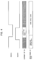
- the first scanning line SCAN-A and the second scanning line SCAN-B are set to be selected status when writing.
- the first scanning line SCAN-A is set to be low level and the second scanning line SCAN-B is set to be high level.
- the signal current Iw corresponding to the intensity information flows through the transistor TFT 1 by connecting the current source CS to the data line DATA while both scanning lines SCAN-A and SCAN-B are in the selected condition.
- the current source CS is a variable current source controlled in accordance with the intensity information.
- the previously mentioned expression (5) is established because the gate-drain of the transistor TFT 1 is short-circuited by the transistor TFT 4, so that the transistor TFT 1 works in the saturation range. Accordingly the voltage Vgs given by the expression (3) occurs between the gate-source of the transistor TFT 1.
- the first scanning line SCAN-A and the second scanning line SCAN-B are set to be non-selected status. Namely in more detail, the transistor TFT 4 is set to be OFF condition by setting the second scanning line SCAN-B to be low level. Thereby the voltage Vgs is restored in the capacitor C.
- the picture element drive circuit is electrically disconnected from the data line DATA by making the transistor TFT 3 to OFF condition by setting the first scanning line SCAN-A to be high level, so that the writing to the other picture element drive circuit can be possible after-words through the data line DATA.
- the data to be outputted as current level of the signal current by the current source CS has to be effective when the second scanning line SCAN-B is in non-selected condition, but afterwards may be an arbitrary level (the writing data for the next picture element, for example).
- the gate and source electrodes of the transistor TFT 2 are commonly connected to the source electrodes of the transistor TFT 1, and those electrodes are formed closely to each other within the small picture element circuit, so that the current flowing through the transistor TFT 2 is determined by the expression (4) if the transistor TFT 2 works in the saturation range.
- This current determined by the expression (4) becomes the drive current Idrv flowing through the OLED device.
- it is only to supply sufficient power potential as the power voltage Vdd so as to establish the expression (5) even considering the voltage drop at the OLED device.
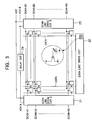
- Fig. 5 is a block diagram showing a construction example of the display apparatus to which the picture element drive circuit of Fig. 1 is applied.
- a vertical start pulse (VSP) is supplied to the scanning line drive circuit A21 constituting of thin film transistors and including a shift register and to the scanning line drive circuit B23 constituting of thin film transistors and including a shift register.
- These scanning line drive circuits A21 and B23 select the first scanning line scanning line SCAN-A1 ⁇ SCAN-AN and the second scanning line SCAN-B1 ⁇ SCAN-BN sequentially in synchronism with vertical clocks (VCKA, VCKB) after receiving the vertical start pulse (VSP).
- VSP vertical start pulse
- the current source CS is provided in the data line drive circuit 22 constituting of thin film transistors, and the current source CS drives the data line DATA with the current level corresponding to the intensity information.
- the current source CS is constituting of a voltage-current converting circuit as briefly depicted in a circle in Fig. 5 and outputs the signal current in response to the voltage representing the intensity information.
- the signal current flows to the picture element on the selected scanning line and is written by the scanning line unit.
- Each of the picture elements starts luminescence by the strength corresponding to the current level.
- the vertical clocks VCKA are slightly delayed relative to the vertical clocks VCKB by a delay circuit 24.
- the second scanning line is set to be non-selected condition in advance of the first scanning line scanning line.
Landscapes
- Engineering & Computer Science (AREA)
- Physics & Mathematics (AREA)
- Computer Hardware Design (AREA)
- General Physics & Mathematics (AREA)
- Theoretical Computer Science (AREA)
- Control Of Indicators Other Than Cathode Ray Tubes (AREA)
- Control Of El Displays (AREA)
- Electroluminescent Light Sources (AREA)
- Devices For Indicating Variable Information By Combining Individual Elements (AREA)
- Thin Film Transistor (AREA)
Abstract
Description

Claims (20)
- An active matrix type display apparatus comprising:a scanning line drive circuit for sequentially selecting scanning lines;a data line drive circuit containing a current source for generating signal current having current level corresponding to an intensity information and for sequentially supplying thus generated signal current to data lines; anda plurality of picture elements provided at each cross point of said data line and said scanning line and each of the picture elements having a current drive type light emitting device which emits light in response to drive current, whereineach of said picture element comprises:an accept section for accepting said signal current from the corresponding data line when corresponding scanning line is selected;a converting section for converting a current level of thus accepted signal current once into corresponding voltage and restoring the converted voltage; anda drive section for supplying the drive current having current level corresponding to the restored voltage to the corresponding light emitting device,said converting section includes: a conversion thin film transistor having a gate electrode, a source electrode, a drain electrode and a channel; anda capacitor connected to said gate electrode of the conversion thin film transistor, wherein said conversion thin film transistor generates at the gate electrode the voltage converted by flowing through said channel the signal current taken through said accept section and said capacitor holds the voltage generated at the gate electrode, said drive section contains:a drive thin film insulated gate type field effect transistor including a gate electrode, a drain electrode, a source electrode and a channel, wherein said drive thin film insulated gate type field effect transistor supplies the drive current through the channel to the light emitting device and the drive current has the current level corresponding to the voltage restored in said capacitor and accepted at the gate electrode of the drive thin film insulated gate type field effect transistor, anda threshold voltage of said drive thin film insulated gate type field effect transistor is set not to become lower than a threshold voltage of said conversion thin film insulated gate type field effect transistor corresponding to the picture element.
- A picture element drive circuit to be provided at each cross point of a data line for supplying a signal current having current level corresponding to an intensity information and a scanning line for supplying a selecting pulse and for driving a current drive type light emitting device which emits light by a drive current, comprising:an accept section for accepting said signal current from the corresponding data line in response to said selecting pulse from said scanning line;a converting section for converting thus accepted signal current once into corresponding voltage and restoring thus converted voltage; anda drive section for supplying the drive current having current level corresponding to the restored voltage to the corresponding light emitting device, and said converting section includes:a conversion thin film transistor having a gate electrode, a source electrode, a drain electrode and a channel; anda capacitor connected to said gate electrode of the conversion thin film transistor, wherein the conversion thin film transistor generates at the gate electrode the voltage converted by flowing through said channel the signal current taken through said accept section and said capacitor holds the voltage generated at the gate electrode of the conversion thin film transistor,said drive section contains:a drive thin film insulated gate type field effect transistor including a gate electrode, a drain electrode, a source electrode and a channel and the drive thin film insulated gate type field effect transistor, wherein the drive thin film insulated gate type field effect transistor supplies the drive current through the channel to the light emitting device and the drive current has the current level corresponding to the voltage restored in the capacitor and accepted at the gate electrode of the drive thin film insulated gate type field effect transistor, anda threshold voltage of said drive thin film insulated gate type field effect transistor is set not to become lower than a threshold voltage of said conversion thin film insulated gate type field effect transistor corresponding to the picture element.
- An apparatus according to claim 1 or a circuit according to claim 2, wherein a gate length of said drive thin film insulated gate type field effect transistor is set not to be shorter than a gate length of said conversion thin film insulated gate type field effect transistor within one picture element.
- An apparatus or a circuit according to any one of the preceding claims, wherein a thickness of a gate insulator of said drive thin film insulated gate type field effect transistor is set not to be thinner than thickness of a gate insulator of said conversion thin film insulated gate type field effect transistor within one picture element.
- An apparatus or a circuit according to any one of the preceding claims, wherein
a threshold voltage of said drive thin film transistor is set not to be lower than a threshold voltage of said conversion thin film insulated gate type field effect transistor within one picture element by adjusting impurity density injected in said channel of the drive thin film insulated gate type field effect transistor. - An apparatus or a circuit according to any one of the preceding claims, wherein said drive thin film insulated gate type field effect transistor works in saturation range and supplies the drive current corresponding to the difference between the threshold voltage and the voltage given to the gate electrode into the light emitting device.
- An apparatus or a circuit according to any one of the preceding claims, wherein a current mirror circuit is constituted by directly connecting the gate electrode of said drive thin film insulated gate type field effect transistor to the gate electrode of the conversion thin film insulated gate type field effect transistor, so that the current level of the signal current and the current level of the drive current are made to be a proportional relation.
- An apparatus or a circuit according to any one of the preceding claims, wherein said accept section includes a switch thin film insulated gate type field effect transistor interposed between the drain electrode and the gate electrode of the conversion thin film insulated gate type field effect transistor,
said switch thin film insulated gate type field effect transistor is made ON when the current level of the signal current is converted into the voltage and generates at the gate electrode of the conversion thin film insulated gate type field effect transistor said voltage referenced with the source electrode by electrically connecting the gate electrode and the drain electrode of the conversion insulated gate type field effect thin film transistor, and said switch thin film insulated gate type field effect transistor is made OFF to disconnect the gate electrode of the conversion thin film insulated gate type field effect transistor and the capacitor when restoring the voltage to said capacitor. - An apparatus or a circuit according to any one of the preceding claims, wherein said light emitting device is an organic electro-luminescence device.
- An apparatus or a circuit according to any one of the preceding claims, wherein said source, drain and channel of both said drive thin film insulated gate type field effect transistor and said conversion thin film insulated gate type field effect transistor are formed with poly-crystal semiconductor thin films.
- A method for driving picture element to be provided at each cross point of a data line for supplying a signal current having current level corresponding to an intensity information and a scanning line for supplying a selecting pulse and for driving a current drive type light emitting device which emits light by a drive current, comprising the steps of:step for accepting said signal current from the corresponding data line in response to said selecting pulse from corresponding scanning line;step for converting thus accepted signal current once into corresponding voltage and restoring the voltage; andstep for driving by supplying the drive current having current level corresponding to the restored voltage to the corresponding light emitting device, andsaid converting step includes:step for using a conversion thin film transistor having a gate electrode, a source electrode, a drain electrode and a channel; anda capacitor connected to said gate electrode of the conversion thin film transistor, wherein the conversion thin film transistor generates at the gate electrode the voltage converted by flowing through said channel the signal current taken through said accepting step and said capacitor holds the voltage generated at the gate electrode,said driving step includes:step for using a drive thin film insulated gate type field effect transistor having a gate electrode, a drain electrode, a source electrode and a channel, wherein said the drive thin film insulated gate type field effect transistor supplies the drive current through the channel to the light emitting device, wherein the drive current has the current level corresponding to the voltage stored in the capacitor and accepted at the gate electrode of the drive thin film insulated gate type field effect transistor, anda threshold voltage of said drive thin film insulated gate type field effect transistor is set not to become lower than a threshold voltage of said conversion thin film insulated gate type field effect transistor corresponding to the picture element.
- A method according to claim 11, wherein
a gate length of said drive thin film insulated gate type field effect transistor is set not to be shorter than a gate length of said conversion thin film insulated gate type field effect transistor within one picture element. - A method according to claim 11 or 12, wherein
a thickness of a gate insulator of said drive thin film insulated gate type field effect transistor is set not to be thinner than thickness of a gate insulator of said conversion thin film insulated gate type field effect transistor within one picture element. - A method according to any one of claims 11 to 13, wherein
a threshold voltage of said drive thin film transistor is set not to be lower than a threshold voltage of said conversion thin film insulated gate type field effect transistor within one picture element by adjusting impurity density injected in said channel of the drive thin film insulated gate type field effect transistor. - A method according to any one of claims 11 to 14, wherein
said drive thin film insulated gate type field effect transistor works in saturation range and supplies the drive current corresponding to the difference between the threshold voltage and the voltage given to the gate electrode into the light emitting device. - A method according to any one of claims 11 to 15, wherein
a current mirror circuit is constituted by directly connecting the gate electrode of said drive thin film insulated gate type field effect transistor to the gate electrode of the conversion thin film insulated gate type field effect transistor, so that the current level of the signal current and the current level of the drive current are made to be a proportional relation. - A method according to any one of claims 11 to 16, whereinsaid accepting step includesa step for using a switch thin film insulated gate type field effect transistor interposed between the drain electrode and the gate electrode of the conversion thin film insulated gate type field effect transistor, wherein said switch thin film insulated gate type field effect transistor is made ON when the current level of the signal current is converted into the voltage and then generates at the gate electrode of the conversion thin film insulated gate type field effect transistor said voltage referenced with the source electrode by electrically connecting the gate electrode and the drain electrode of the conversion insulated gate type field effect thin film transistor, andsaid switch thin film insulated gate type field effect transistor is made OFF to disconnect the gate electrode of the conversion thin film insulated gate type field effect transistor and the capacitor when restoring the voltage to said capacitor.
- A method according to any one of claims 11 to 17, wherein said light emitting device is an organic electro-luminescence device.
- A method according to any one of claims 11 to 18, wherein
said source, drain and channel of both said drive thin film insulated gate type field effect transistor and said conversion thin film insulated gate type field effect transistor are formed with poly-crystal semiconductor thin films. - An active matrix type display apparatus comprising:a scanning line drive circuit for sequentially selecting scanning lines;a data line drive circuit for sequentially supplying signal current corresponding to an intensity information to data lines; anda plurality of picture elements provided at each cross point of said data line and said scanning line and each of the picture elements having a current drive type light emitting device which emits light in response to drive current corresponding to said signal current, whereineach of said picture element comprises:an input thin film transistor connected to said data line;a conversion thin film transistor connected to said input thin film transistor for converting said signal current on said data line to corresponding voltage;a switch thin film transistor connected between a gate electrode and a source electrode of said conversion thin film transistor,a capacitor connected to said gate electrode of said conversion thin film transistor for restoring said corresponding voltage; anda drive thin film transistor connected to said light emitting device and to said capacitor, wherein a threshold voltage of said drive thin film transistor is set not to become lower than a threshold voltage of said conversion thin film transistor within one the picture element.
Applications Claiming Priority (2)
| Application Number | Priority Date | Filing Date | Title |
|---|---|---|---|
| JP32763799A JP2001147659A (en) | 1999-11-18 | 1999-11-18 | Display device |
| JP32763799 | 1999-11-18 |
Publications (2)
| Publication Number | Publication Date |
|---|---|
| EP1102234A2 true EP1102234A2 (en) | 2001-05-23 |
| EP1102234A3 EP1102234A3 (en) | 2001-09-12 |
Family
ID=18201285
Family Applications (1)
| Application Number | Title | Priority Date | Filing Date |
|---|---|---|---|
| EP00310214A Withdrawn EP1102234A3 (en) | 1999-11-18 | 2000-11-17 | Active matrix type display apparatus and drive circuit thereof |
Country Status (4)
| Country | Link |
|---|---|
| US (1) | US6501466B1 (en) |
| EP (1) | EP1102234A3 (en) |
| JP (1) | JP2001147659A (en) |
| KR (1) | KR20010051698A (en) |
Cited By (70)
| Publication number | Priority date | Publication date | Assignee | Title |
|---|---|---|---|---|
| KR20010051698A (en) * | 1999-11-18 | 2001-06-25 | 이데이 노부유끼 | Display device |
| WO2003038790A3 (en) * | 2001-10-31 | 2003-06-12 | Cambridge Display Tech Ltd | Display drivers for electro-optic displays |
| US6693385B2 (en) | 2001-03-22 | 2004-02-17 | Semiconductor Energy Laboratory Co., Ltd. | Method of driving a display device |
| EP1291841A3 (en) * | 2001-09-10 | 2004-04-28 | Seiko Epson Corporation | Unit circuit, electronic circuit, electronic apparatus, electro-optic apparatus, driving method, and electronic equipment |
| US6777710B1 (en) | 2001-02-26 | 2004-08-17 | Semiconductor Energy Laboratory Co., Ltd. | Organic light emitting device with constant luminance |
| US6798148B2 (en) | 2002-03-01 | 2004-09-28 | Semiconductor Energy Laboratory Co., Ltd. | Display device, light emitting device, and electronic equipment |
| US6876350B2 (en) | 2001-08-10 | 2005-04-05 | Semiconductor Energy Laboratory Co., Ltd. | Display device and electronic equipment using the same |
| WO2005064582A2 (en) | 2003-12-23 | 2005-07-14 | Thomson Licensing | Circuit and method for driving a light-emitting display |
| US6930328B2 (en) | 2002-04-11 | 2005-08-16 | Semiconductor Energy Laboratory Co., Ltd. | Semiconductor device and method of manufacturing the same |
| EP1589518A2 (en) | 2004-04-19 | 2005-10-26 | Sony Corporation | Active matrix display device and method of driving the same |
| US6963336B2 (en) | 2001-10-31 | 2005-11-08 | Semiconductor Energy Laboratory Co., Ltd. | Signal line driving circuit and light emitting device |
| US7005675B2 (en) | 2002-05-31 | 2006-02-28 | Semiconductor Energy Laboratory Co., Ltd. | Light-emitting device, method for driving light-emitting device and element board |
| US7046240B2 (en) | 2001-08-29 | 2006-05-16 | Semiconductor Energy Laboratory Co., Ltd. | Light emitting device, method of driving a light emitting device, element substrate, and electronic equipment |
| EP1465146A3 (en) * | 2003-03-31 | 2006-05-17 | SANYO ELECTRIC Co., Ltd. | Light emitting display apparatus with circuit for improving writing operation |
| US7102161B2 (en) | 2001-10-09 | 2006-09-05 | Semiconductor Energy Laboratory Co., Ltd. | Switching element, display device using the switching element, and light emitting device |
| US7108574B2 (en) | 2001-09-28 | 2006-09-19 | Semiconductor Energy Laboratory Co., Ltd. | Light emitting device and method of manufacturing the same |
| US7138967B2 (en) | 2001-09-21 | 2006-11-21 | Semiconductor Energy Laboratory Co., Ltd. | Display device and driving method thereof |
| US7170094B2 (en) | 2001-09-21 | 2007-01-30 | Semiconductor Energy Laboratory Co., Ltd. | Light emitting device, driving method of light emitting device and electronic device |
| US7170479B2 (en) | 2002-05-17 | 2007-01-30 | Semiconductor Energy Laboratory Co., Ltd. | Display device and driving method thereof |
| US7180479B2 (en) | 2001-10-30 | 2007-02-20 | Semiconductor Energy Laboratory Co., Ltd. | Signal line drive circuit and light emitting device and driving method therefor |
| US7184034B2 (en) | 2002-05-17 | 2007-02-27 | Semiconductor Energy Laboratory Co., Ltd. | Display device |
| US7193619B2 (en) | 2001-10-31 | 2007-03-20 | Semiconductor Energy Laboratory Co., Ltd. | Signal line driving circuit and light emitting device |
| CN1313997C (en) * | 2003-04-01 | 2007-05-02 | 三星Sdi株式会社 | Luminous display device display panel and its driving method |
| CN1316442C (en) * | 2003-03-31 | 2007-05-16 | 精工爱普生株式会社 | Pixel circuit, electronic device and electronic apparatus |
| CN1323383C (en) * | 2003-04-01 | 2007-06-27 | 三星Sdi株式会社 | Light-emitting display, display screen and driving method thereof |
| US7250928B2 (en) | 2001-09-17 | 2007-07-31 | Semiconductor Energy Laboratory Co., Ltd. | Light emitting device, method of driving a light emitting device, and electronic equipment |
| US7259735B2 (en) | 2002-12-12 | 2007-08-21 | Seiko Epson Corporation | Electro-optical device, method of driving electro-optical device, and electronic apparatus |
| CN100354908C (en) * | 2002-09-25 | 2007-12-12 | 三星电子株式会社 | Organic luminous displaying device and manufacturing method thereof |
| CN100362555C (en) * | 2003-11-20 | 2008-01-16 | 精工爱普生株式会社 | Pixel circuit, electro-optical device and electronic equipment thereof |
| US7333099B2 (en) | 2003-01-06 | 2008-02-19 | Semiconductor Energy Laboratory Co., Ltd. | Electronic circuit, display device, and electronic apparatus |
| CN100375144C (en) * | 2002-11-06 | 2008-03-12 | 三菱电机株式会社 | Sample hold circuit and image display device using it |
| US7348947B2 (en) | 2003-01-07 | 2008-03-25 | Semiconductor Energy Laboratory Co., Ltd. | Circuit, display device, and electronic apparatus |
| CN100378784C (en) * | 2004-07-28 | 2008-04-02 | 三星Sdi株式会社 | Pixel circuit and organic light emitting display using the pixel circuit |
| CN100378777C (en) * | 2002-10-17 | 2008-04-02 | 精工爱普生株式会社 | Electronic circuits, electro-optical devices and electronic instruments |
| US7365715B2 (en) | 2002-12-27 | 2008-04-29 | Semiconductor Energy Laboratory Co., Ltd. | Electronic circuit, electronic device and personal computer |
| US7372437B2 (en) | 2001-10-12 | 2008-05-13 | Semiconductor Energy Laboratory Co., Ltd. | Drive circuit, display device using the drive circuit and electronic apparatus using the display device |
| CN100416635C (en) * | 2001-10-30 | 2008-09-03 | 株式会社半导体能源研究所 | Signal line driving circuit, light emitting device and driving method thereof |
| CN100416636C (en) * | 2001-10-30 | 2008-09-03 | 株式会社半导体能源研究所 | Signal line driving circuit, light emitting device and driving method thereof |
| CN100418123C (en) * | 2003-02-24 | 2008-09-10 | 奇美电子股份有限公司 | display device |
| CN100419839C (en) * | 2005-03-02 | 2008-09-17 | 立锜科技股份有限公司 | Method and circuit for operating passive matrix organic light emitting diode display panel |
| US7474285B2 (en) | 2002-05-17 | 2009-01-06 | Semiconductor Energy Laboratory Co., Ltd. | Display apparatus and driving method thereof |
| US7511687B2 (en) | 2002-05-17 | 2009-03-31 | Semiconductor Energy Laboratory Co., Ltd. | Display device, electronic apparatus and navigation system |
| CN100481176C (en) * | 2002-08-30 | 2009-04-22 | 株式会社半导体能源研究所 | Current source circuit, display device using the same and driving method thereof |
| US7532209B2 (en) | 2002-05-17 | 2009-05-12 | Semiconductor Energy Laboratory Co., Ltd. | Display apparatus and driving method thereof |
| EP1178462A3 (en) * | 2000-06-22 | 2009-06-10 | Semiconductor Energy Laboratory Co., Ltd. | Active matrix electroluminescent display device |
| US7561147B2 (en) | 2003-05-07 | 2009-07-14 | Toshiba Matsushita Display Technology Co., Ltd. | Current output type of semiconductor circuit, source driver for display drive, display device, and current output method |
| US7583032B2 (en) | 2001-09-21 | 2009-09-01 | Semiconductor Energy Laboratory Co., Ltd. | Semiconductor device |
| US7586505B2 (en) | 2001-09-28 | 2009-09-08 | Semiconductor Energy Laboratory Co., Ltd. | Light emitting device and electronic apparatus using the same |
| EP1571643A4 (en) * | 2002-11-20 | 2009-11-25 | Toshiba Matsushita Display Tec | ORGANIC ELECTROLUMINESCENT DISPLAY AND ACTIVE MATRIX SUBSTRATE |
| US7629611B2 (en) | 2001-11-09 | 2009-12-08 | Semiconductor Energy Laboratory Co., Ltd. | Semiconductor element, electronic device |
| US7649516B2 (en) | 2001-07-16 | 2010-01-19 | Semiconductor Energy Laboratory Co., Ltd. | Light emitting device |
| US7688291B2 (en) | 2001-09-28 | 2010-03-30 | Semiconductor Energy Laboratory Co., Ltd. | Light emitting device and electronic apparatus using the same |
| CN1898719B (en) * | 2003-12-23 | 2010-04-21 | 汤姆森特许公司 | Apparatus for displaying images on an active matrix |
| US7714816B2 (en) | 2005-03-31 | 2010-05-11 | Semiconductor Energy Laboratory Co., Ltd. | Display device, display module, electronic apparatus and driving method of the display device |
| US7723721B2 (en) | 2001-11-09 | 2010-05-25 | Semiconductor Energy Laboratory Co., Ltd. | Light emitting device having TFT |
| US7728653B2 (en) | 2002-03-06 | 2010-06-01 | Semiconductor Energy Laboratory Co., Ltd. | Display and method of driving the same |
| US7742019B2 (en) | 2002-04-26 | 2010-06-22 | Toshiba Matsushita Display Technology Co., Ltd. | Drive method of el display apparatus |
| US7777698B2 (en) | 2002-04-26 | 2010-08-17 | Toshiba Matsushita Display Technology, Co., Ltd. | Drive method of EL display panel |
| CN1503211B (en) * | 2002-11-27 | 2010-10-06 | 精工爱普生株式会社 | Electro-optical device, driving method of electro-optical device, and electronic device |
| US7817149B2 (en) | 2002-04-26 | 2010-10-19 | Toshiba Matsushita Display Technology Co., Ltd. | Semiconductor circuits for driving current-driven display and display |
| US7961160B2 (en) | 2003-07-31 | 2011-06-14 | Semiconductor Energy Laboratory Co., Ltd. | Display device, a driving method of a display device, and a semiconductor integrated circuit incorporated in a display device |
| US8477085B2 (en) | 2006-12-15 | 2013-07-02 | Semiconductor Energy Laboratory Co., Ltd. | Semiconductor device and driving method thereof |
| US8659529B2 (en) | 2003-01-17 | 2014-02-25 | Semiconductor Energy Laboratory Co., Ltd. | Current source circuit, a signal line driver circuit and a driving method thereof and a light emitting device |
| US8941314B2 (en) | 2001-10-26 | 2015-01-27 | Semiconductor Energy Laboratory Co., Ltd. | Light-emitting device and driving method thereof |
| US8988400B2 (en) | 2005-10-18 | 2015-03-24 | Semiconductor Energy Laboratory Co., Ltd. | Display device and driving method thereof |
| CN104751775A (en) * | 2013-12-27 | 2015-07-01 | 昆山工研院新型平板显示技术中心有限公司 | Pixel circuit with compensation function, driving method of pixel circuit and display circuit with compensation function |
| EP1971975B1 (en) * | 2006-01-09 | 2015-10-21 | Ignis Innovation Inc. | Method and system for driving an active matrix display circuit |
| WO2017049849A1 (en) * | 2015-09-23 | 2017-03-30 | 京东方科技集团股份有限公司 | Drive circuit, drive method therefor and display device |
| US10679550B2 (en) | 2001-10-24 | 2020-06-09 | Semiconductor Energy Laboratory Co., Ltd. | Display device |
| CN111710304A (en) * | 2020-07-17 | 2020-09-25 | 京东方科技集团股份有限公司 | Pixel driving circuit and driving method thereof, and display device |
Families Citing this family (295)
| Publication number | Priority date | Publication date | Assignee | Title |
|---|---|---|---|---|
| AU752330B2 (en) * | 1998-01-06 | 2002-09-19 | Trustees Of Boston University | Decorated red blood cells |
| JP2000310969A (en) * | 1999-02-25 | 2000-11-07 | Canon Inc | Image display device and driving method of image display device |
| US6859193B1 (en) * | 1999-07-14 | 2005-02-22 | Sony Corporation | Current drive circuit and display device using the same, pixel circuit, and drive method |
| EP1170718B1 (en) * | 2000-07-07 | 2010-06-09 | Seiko Epson Corporation | Current sampling circuit for organic electroluminescent display |
| US6879110B2 (en) | 2000-07-27 | 2005-04-12 | Semiconductor Energy Laboratory Co., Ltd. | Method of driving display device |
| JP2003195815A (en) | 2000-11-07 | 2003-07-09 | Sony Corp | Active matrix type display device and active matrix type organic electroluminescence display device |
| US7015882B2 (en) * | 2000-11-07 | 2006-03-21 | Sony Corporation | Active matrix display and active matrix organic electroluminescence display |
| JP2002182612A (en) * | 2000-12-11 | 2002-06-26 | Sony Corp | Image display device |
| JP2002189445A (en) * | 2000-12-19 | 2002-07-05 | Sony Corp | Image display device and driving method thereof |
| JP3593982B2 (en) * | 2001-01-15 | 2004-11-24 | ソニー株式会社 | Active matrix type display device, active matrix type organic electroluminescence display device, and driving method thereof |
| US7569849B2 (en) | 2001-02-16 | 2009-08-04 | Ignis Innovation Inc. | Pixel driver circuit and pixel circuit having the pixel driver circuit |
| US6753654B2 (en) | 2001-02-21 | 2004-06-22 | Semiconductor Energy Laboratory Co., Ltd. | Light emitting device and electronic appliance |
| JPWO2002075709A1 (en) * | 2001-03-21 | 2004-07-08 | キヤノン株式会社 | Driver circuit for active matrix light emitting device |
| US6661180B2 (en) * | 2001-03-22 | 2003-12-09 | Semiconductor Energy Laboratory Co., Ltd. | Light emitting device, driving method for the same and electronic apparatus |
| JP3608613B2 (en) * | 2001-03-28 | 2005-01-12 | 株式会社日立製作所 | Display device |
| US7112844B2 (en) * | 2001-04-19 | 2006-09-26 | Semiconductor Energy Laboratory Co., Ltd. | Semiconductor device and manufacturing method thereof |
| JP3610923B2 (en) * | 2001-05-30 | 2005-01-19 | ソニー株式会社 | Active matrix display device, active matrix organic electroluminescence display device, and driving method thereof |
| JP2003005710A (en) * | 2001-06-25 | 2003-01-08 | Nec Corp | Current driving circuit and image display device |
| JP2003043994A (en) | 2001-07-27 | 2003-02-14 | Canon Inc | Active matrix display |
| US7012597B2 (en) * | 2001-08-02 | 2006-03-14 | Seiko Epson Corporation | Supply of a programming current to a pixel |
| KR100819138B1 (en) * | 2001-08-25 | 2008-04-21 | 엘지.필립스 엘시디 주식회사 | Driving device of electroluminescence panel and driving method thereof |
| US7088052B2 (en) * | 2001-09-07 | 2006-08-08 | Semiconductor Energy Laboratory Co., Ltd. | Light emitting device and method of driving the same |
| JP2005505802A (en) * | 2001-09-20 | 2005-02-24 | パイオニア株式会社 | Light emitting element drive circuit |
| JP3691475B2 (en) * | 2001-09-28 | 2005-09-07 | 株式会社半導体エネルギー研究所 | Light emitting device |
| JP4176790B2 (en) * | 2001-09-28 | 2008-11-05 | 株式会社半導体エネルギー研究所 | LIGHT EMITTING DEVICE AND ELECTRONIC DEVICE |
| JP3899886B2 (en) * | 2001-10-10 | 2007-03-28 | 株式会社日立製作所 | Image display device |
| DE10151440C1 (en) | 2001-10-18 | 2003-02-06 | Siemens Ag | Organic electronic component for implementing an encapsulated partially organic electronic component has components like a flexible foil as an antenna, a diode or capacitor and an organic transistor. |
| KR100433216B1 (en) * | 2001-11-06 | 2004-05-27 | 엘지.필립스 엘시디 주식회사 | Apparatus and method of driving electro luminescence panel |
| JP2003150107A (en) * | 2001-11-09 | 2003-05-23 | Sharp Corp | Display device and driving method thereof |
| CN101009322B (en) * | 2001-11-09 | 2012-06-27 | 株式会社半导体能源研究所 | Light-emitting device |
| US20030103022A1 (en) * | 2001-11-09 | 2003-06-05 | Yukihiro Noguchi | Display apparatus with function for initializing luminance data of optical element |
| US7141817B2 (en) * | 2001-11-30 | 2006-11-28 | Semiconductor Energy Laboratory Co., Ltd. | Light emitting device |
| JP2003177709A (en) | 2001-12-13 | 2003-06-27 | Seiko Epson Corp | Pixel circuit for light emitting element |
| JP2003186437A (en) * | 2001-12-18 | 2003-07-04 | Sanyo Electric Co Ltd | Display device |
| US6847171B2 (en) * | 2001-12-21 | 2005-01-25 | Seiko Epson Corporation | Organic electroluminescent device compensated pixel driver circuit |
| JP2003195810A (en) | 2001-12-28 | 2003-07-09 | Casio Comput Co Ltd | Driving circuit, driving device, and driving method of optical element |
| JP2003255899A (en) * | 2001-12-28 | 2003-09-10 | Sanyo Electric Co Ltd | Display device |
| KR100453633B1 (en) * | 2001-12-29 | 2004-10-20 | 엘지.필립스 엘시디 주식회사 | an active matrix organic electroluminescence display and a manufacturing method of the same |
| KR100453634B1 (en) * | 2001-12-29 | 2004-10-20 | 엘지.필립스 엘시디 주식회사 | an active matrix organic electroluminescence display |
| KR100453635B1 (en) * | 2001-12-29 | 2004-10-20 | 엘지.필립스 엘시디 주식회사 | an active matrix organic electroluminescence display device |
| KR100426031B1 (en) * | 2001-12-29 | 2004-04-03 | 엘지.필립스 엘시디 주식회사 | an active matrix organic electroluminescence display and a manufacturing method of the same |
| GB2384100B (en) * | 2002-01-09 | 2005-10-26 | Seiko Epson Corp | An electronic circuit for controlling the current supply to an element |
| JP3953330B2 (en) | 2002-01-25 | 2007-08-08 | 三洋電機株式会社 | Display device |
| JP3723507B2 (en) * | 2002-01-29 | 2005-12-07 | 三洋電機株式会社 | Driving circuit |
| JP2003295825A (en) * | 2002-02-04 | 2003-10-15 | Sanyo Electric Co Ltd | Display device |
| JP2003308030A (en) | 2002-02-18 | 2003-10-31 | Sanyo Electric Co Ltd | Display device |
| KR100469070B1 (en) * | 2002-02-19 | 2005-02-02 | 재단법인서울대학교산학협력재단 | Picture Element Structure of Active Matrix Organic Emitting Diode Display |
| JP4024557B2 (en) * | 2002-02-28 | 2007-12-19 | 株式会社半導体エネルギー研究所 | Light emitting device, electronic equipment |
| JP2003332058A (en) * | 2002-03-05 | 2003-11-21 | Sanyo Electric Co Ltd | Electroluminescent panel and method of manufacturing the same |
| JP2003258094A (en) * | 2002-03-05 | 2003-09-12 | Sanyo Electric Co Ltd | Wiring structure, method of manufacturing the same, and display device |
| JP2003257645A (en) * | 2002-03-05 | 2003-09-12 | Sanyo Electric Co Ltd | Light emitting device and manufacturing method thereof |
| US7876294B2 (en) | 2002-03-05 | 2011-01-25 | Nec Corporation | Image display and its control method |
| CN100517422C (en) * | 2002-03-07 | 2009-07-22 | 三洋电机株式会社 | Distributing structure, its manufacturing method and optical equipment |
| JP3671012B2 (en) * | 2002-03-07 | 2005-07-13 | 三洋電機株式会社 | Display device |
| JP3837344B2 (en) * | 2002-03-11 | 2006-10-25 | 三洋電機株式会社 | Optical element and manufacturing method thereof |
| KR100461467B1 (en) * | 2002-03-13 | 2004-12-13 | 엘지.필립스 엘시디 주식회사 | an active matrix organic electroluminescence display device |
| TW575851B (en) * | 2002-03-22 | 2004-02-11 | Ind Tech Res Inst | Elemental circuit for active matrix of current driving device |
| KR100643563B1 (en) * | 2002-03-26 | 2006-11-10 | 엘지.필립스 엘시디 주식회사 | Active matrix organic electroluminescent device |
| JP4046267B2 (en) * | 2002-03-26 | 2008-02-13 | 株式会社半導体エネルギー研究所 | Display device |
| KR100488835B1 (en) * | 2002-04-04 | 2005-05-11 | 산요덴키가부시키가이샤 | Semiconductor device and display device |
| KR100452114B1 (en) * | 2002-04-15 | 2004-10-12 | 한국과학기술원 | Pixel circuit and Organic Light Eitting Dode display using the same |
| JP3637911B2 (en) | 2002-04-24 | 2005-04-13 | セイコーエプソン株式会社 | Electronic device, electronic apparatus, and driving method of electronic device |
| JP2003316321A (en) * | 2002-04-25 | 2003-11-07 | Dainippon Printing Co Ltd | Display device and electronic equipment |
| JP4693338B2 (en) * | 2002-05-17 | 2011-06-01 | 株式会社半導体エネルギー研究所 | Display device |
| KR100640049B1 (en) * | 2002-06-07 | 2006-10-31 | 엘지.필립스 엘시디 주식회사 | Method and apparatus for driving an organic light emitting display device |
| JP3918642B2 (en) | 2002-06-07 | 2007-05-23 | カシオ計算機株式会社 | Display device and driving method thereof |
| KR100441530B1 (en) * | 2002-06-11 | 2004-07-23 | 삼성에스디아이 주식회사 | Display device of organic electro luminescent and driving method there of |
| JP2004070293A (en) * | 2002-06-12 | 2004-03-04 | Seiko Epson Corp | Electronic device, method of driving electronic device, and electronic apparatus |
| CN100517441C (en) * | 2002-06-19 | 2009-07-22 | 三菱电机株式会社 | Display device |
| JP4610843B2 (en) | 2002-06-20 | 2011-01-12 | カシオ計算機株式会社 | Display device and driving method of display device |
| KR100868642B1 (en) * | 2002-07-19 | 2008-11-12 | 매그나칩 반도체 유한회사 | Active organic EL display device |
| JP4123084B2 (en) * | 2002-07-31 | 2008-07-23 | セイコーエプソン株式会社 | Electronic circuit, electro-optical device, and electronic apparatus |
| JP3829778B2 (en) * | 2002-08-07 | 2006-10-04 | セイコーエプソン株式会社 | Electronic circuit, electro-optical device, and electronic apparatus |
| JP4103500B2 (en) | 2002-08-26 | 2008-06-18 | カシオ計算機株式会社 | Display device and display panel driving method |
| TW558699B (en) * | 2002-08-28 | 2003-10-21 | Au Optronics Corp | Driving circuit and method for light emitting device |
| JP4144462B2 (en) * | 2002-08-30 | 2008-09-03 | セイコーエプソン株式会社 | Electro-optical device and electronic apparatus |
| JP2004109991A (en) * | 2002-08-30 | 2004-04-08 | Sanyo Electric Co Ltd | Display driving circuit |
| JP2004145278A (en) * | 2002-08-30 | 2004-05-20 | Seiko Epson Corp | Electronic circuit, method of driving electronic circuit, electro-optical device, method of driving electro-optical device, and electronic apparatus |
| JP4416456B2 (en) * | 2002-09-02 | 2010-02-17 | キヤノン株式会社 | Electroluminescence device |
| TW571281B (en) * | 2002-09-12 | 2004-01-11 | Au Optronics Corp | Driving circuit and method for a display device and display device therewith |
| KR100450761B1 (en) * | 2002-09-14 | 2004-10-01 | 한국전자통신연구원 | Active matrix organic light emission diode display panel circuit |
| JP2004139042A (en) | 2002-09-24 | 2004-05-13 | Seiko Epson Corp | Electronic circuit, electro-optical device, method of driving electro-optical device, and electronic apparatus |
| JP2004117820A (en) * | 2002-09-26 | 2004-04-15 | Seiko Epson Corp | Electronic circuits, electronic devices and electronic equipment |
| JP2004145300A (en) | 2002-10-03 | 2004-05-20 | Seiko Epson Corp | Electronic circuit, method of driving electronic circuit, electronic device, electro-optical device, method of driving electro-optical device, and electronic apparatus |
| JP4467909B2 (en) * | 2002-10-04 | 2010-05-26 | シャープ株式会社 | Display device |
| JP4409821B2 (en) | 2002-11-21 | 2010-02-03 | 奇美電子股▲ふん▼有限公司 | EL display device |
| JP2004198493A (en) * | 2002-12-16 | 2004-07-15 | Seiko Epson Corp | Method for driving electronic circuit, method for driving electronic device, method for driving electro-optical device, and electronic apparatus |
| US7271784B2 (en) | 2002-12-18 | 2007-09-18 | Semiconductor Energy Laboratory Co., Ltd. | Display device and driving method thereof |
| JP3810364B2 (en) | 2002-12-19 | 2006-08-16 | 松下電器産業株式会社 | Display device driver |
| TWI405156B (en) * | 2003-01-06 | 2013-08-11 | Semiconductor Energy Lab | Circuit, display device, and electronic device |
| US6975293B2 (en) * | 2003-01-31 | 2005-12-13 | Faraday Technology Corp. | Active matrix LED display driving circuit |
| JP4048969B2 (en) * | 2003-02-12 | 2008-02-20 | セイコーエプソン株式会社 | Electro-optical device driving method and electronic apparatus |
| CA2419704A1 (en) | 2003-02-24 | 2004-08-24 | Ignis Innovation Inc. | Method of manufacturing a pixel with organic light-emitting diode |
| JP3952965B2 (en) | 2003-02-25 | 2007-08-01 | カシオ計算機株式会社 | Display device and driving method of display device |
| JP4502585B2 (en) * | 2003-03-03 | 2010-07-14 | 三洋電機株式会社 | Electroluminescence display device |
| JP4338997B2 (en) | 2003-03-17 | 2009-10-07 | 株式会社半導体エネルギー研究所 | Method for manufacturing display device |
| JP2004294865A (en) | 2003-03-27 | 2004-10-21 | Sanyo Electric Co Ltd | Display circuit |
| JP2004303522A (en) | 2003-03-31 | 2004-10-28 | Fujitsu Display Technologies Corp | Display device and method of manufacturing the same |
| JP2005128476A (en) * | 2003-04-17 | 2005-05-19 | Sanyo Electric Co Ltd | Display device |
| CN100357999C (en) * | 2003-04-24 | 2007-12-26 | 友达光电股份有限公司 | Organic Light Emitting Diode Driver Circuit |
| CN100367333C (en) * | 2003-04-24 | 2008-02-06 | 友达光电股份有限公司 | Method of driving organic light emitting diode |
| JP5122131B2 (en) * | 2003-04-25 | 2013-01-16 | 統寶光電股▲ふん▼有限公司 | Method and apparatus for driving an active matrix display panel |
| US6919681B2 (en) * | 2003-04-30 | 2005-07-19 | Eastman Kodak Company | Color OLED display with improved power efficiency |
| US6961032B2 (en) * | 2003-05-06 | 2005-11-01 | Eastman Kodak Company | Reducing the effects of shorts in pixels of an active matrix organic electroluminescent device |
| CN1820295A (en) * | 2003-05-07 | 2006-08-16 | 东芝松下显示技术有限公司 | El display and its driving method |
| JP4425574B2 (en) * | 2003-05-16 | 2010-03-03 | 株式会社半導体エネルギー研究所 | Element substrate and light emitting device |
| JP3772889B2 (en) | 2003-05-19 | 2006-05-10 | セイコーエプソン株式会社 | Electro-optical device and driving device thereof |
| JP4016962B2 (en) | 2003-05-19 | 2007-12-05 | セイコーエプソン株式会社 | Electro-optical device and driving method of electro-optical device |
| JP2005010747A (en) * | 2003-05-22 | 2005-01-13 | Sanyo Electric Co Ltd | Display device |
| JP2005017977A (en) * | 2003-06-30 | 2005-01-20 | Casio Comput Co Ltd | CURRENT GENERATION SUPPLY CIRCUIT AND DISPLAY DEVICE PROVIDED WITH THE CURRENT GENERATION SUPPLY CIRCUIT |
| JP4346350B2 (en) * | 2003-05-28 | 2009-10-21 | 三菱電機株式会社 | Display device |
| CN100353399C (en) * | 2003-05-29 | 2007-12-05 | 友达光电股份有限公司 | Active organic electroluminescence display unit |
| JP2004361753A (en) * | 2003-06-05 | 2004-12-24 | Chi Mei Electronics Corp | Image display device |
| TWI253614B (en) | 2003-06-20 | 2006-04-21 | Sanyo Electric Co | Display device |
| US8378939B2 (en) * | 2003-07-11 | 2013-02-19 | Semiconductor Energy Laboratory Co., Ltd. | Semiconductor device |
| US8937580B2 (en) * | 2003-08-08 | 2015-01-20 | Semiconductor Energy Laboratory Co., Ltd. | Driving method of light emitting device and light emitting device |
| JP2005099712A (en) | 2003-08-28 | 2005-04-14 | Sharp Corp | Display device drive circuit and display device |
| CA2443206A1 (en) | 2003-09-23 | 2005-03-23 | Ignis Innovation Inc. | Amoled display backplanes - pixel driver circuits, array architecture, and external compensation |
| US7193588B2 (en) * | 2003-09-29 | 2007-03-20 | Wintek Corporation | Active matrix organic electroluminescence display driving circuit |
| US7310077B2 (en) * | 2003-09-29 | 2007-12-18 | Michael Gillis Kane | Pixel circuit for an active matrix organic light-emitting diode display |
| US7633470B2 (en) | 2003-09-29 | 2009-12-15 | Michael Gillis Kane | Driver circuit, as for an OLED display |
| JP4049085B2 (en) * | 2003-11-11 | 2008-02-20 | セイコーエプソン株式会社 | Pixel circuit driving method, pixel circuit, and electronic device |
| KR100600865B1 (en) * | 2003-11-19 | 2006-07-14 | 삼성에스디아이 주식회사 | Active element display device including electromagnetic wave shielding means |
| JP3966270B2 (en) | 2003-11-21 | 2007-08-29 | セイコーエプソン株式会社 | Pixel circuit driving method, electro-optical device, and electronic apparatus |
| JP3922246B2 (en) | 2003-11-21 | 2007-05-30 | セイコーエプソン株式会社 | CURRENT GENERATION CIRCUIT, CURRENT GENERATION CIRCUIT CONTROL METHOD, ELECTRO-OPTICAL DEVICE, AND ELECTRONIC DEVICE |
| JP4785373B2 (en) * | 2003-11-27 | 2011-10-05 | 株式会社半導体エネルギー研究所 | Display device |
| KR100578791B1 (en) * | 2003-11-29 | 2006-05-11 | 삼성에스디아이 주식회사 | Light emitting display device and driving method thereof |
| US7405713B2 (en) | 2003-12-25 | 2008-07-29 | Semiconductor Energy Laboratory Co., Ltd. | Light emitting device and electronic equipment using the same |
| JP2005242323A (en) * | 2004-01-26 | 2005-09-08 | Semiconductor Energy Lab Co Ltd | Display device and driving method thereof |
| US7339560B2 (en) * | 2004-02-12 | 2008-03-04 | Au Optronics Corporation | OLED pixel |
| US7173585B2 (en) | 2004-03-10 | 2007-02-06 | Wintek Corporation | Active matrix display driving circuit |
| JP4687943B2 (en) | 2004-03-18 | 2011-05-25 | 奇美電子股▲ふん▼有限公司 | Image display device |
| JP4665419B2 (en) | 2004-03-30 | 2011-04-06 | カシオ計算機株式会社 | Pixel circuit board inspection method and inspection apparatus |
| US6977470B2 (en) * | 2004-04-28 | 2005-12-20 | Au Optronics Corp. | Current-driven OLED pixel |
| KR100627333B1 (en) | 2004-04-29 | 2006-09-25 | 삼성에스디아이 주식회사 | Organic EL light emitting cell and its manufacturing method |
| TWI288900B (en) | 2004-04-30 | 2007-10-21 | Fujifilm Corp | Active matrix type display device |
| KR101057206B1 (en) * | 2004-04-30 | 2011-08-16 | 엘지디스플레이 주식회사 | Organic light emitting device |
| JP4660116B2 (en) | 2004-05-20 | 2011-03-30 | 三洋電機株式会社 | Current-driven pixel circuit |
| TWI272560B (en) * | 2004-05-21 | 2007-02-01 | Au Optronics Corp | Data driving circuit and active matrix organic light emitting diode display |
| KR100658616B1 (en) | 2004-05-31 | 2006-12-15 | 삼성에스디아이 주식회사 | Light emitting display device, display panel and driving method thereof |
| JP2005340721A (en) * | 2004-05-31 | 2005-12-08 | Anelva Corp | Method for depositing high dielectric constant dielectric films |
| US20050275352A1 (en) * | 2004-06-14 | 2005-12-15 | Au Optronics Corporation. | Redundant storage capacitor and method for repairing OLED pixels and driving circuits |
| KR100636503B1 (en) * | 2004-06-25 | 2006-10-18 | 삼성에스디아이 주식회사 | Light emitting display device and manufacturing method thereof |
| CA2472671A1 (en) | 2004-06-29 | 2005-12-29 | Ignis Innovation Inc. | Voltage-programming scheme for current-driven amoled displays |
| EP1780583B1 (en) | 2004-07-14 | 2013-12-25 | Sharp Kabushiki Kaisha | Active matrix substrate and drive circuit thereof |
| US7046225B2 (en) * | 2004-08-06 | 2006-05-16 | Chen-Jean Chou | Light emitting device display circuit and drive method thereof |
| US7053875B2 (en) * | 2004-08-21 | 2006-05-30 | Chen-Jean Chou | Light emitting device display circuit and drive method thereof |
| US7589706B2 (en) * | 2004-09-03 | 2009-09-15 | Chen-Jean Chou | Active matrix light emitting device display and drive method thereof |
| US7105855B2 (en) * | 2004-09-20 | 2006-09-12 | Eastman Kodak Company | Providing driving current arrangement for OLED device |
| US7589707B2 (en) * | 2004-09-24 | 2009-09-15 | Chen-Jean Chou | Active matrix light emitting device display pixel circuit and drive method |
| US20060071887A1 (en) * | 2004-10-01 | 2006-04-06 | Chen-Jean Chou | Active matrix display and drive method thereof |
| EP2383721B1 (en) * | 2004-11-16 | 2015-04-08 | Ignis Innovation Inc. | System and Driving Method for Active Matrix Light Emitting Device Display |
| CA2490848A1 (en) * | 2004-11-16 | 2006-05-16 | Arokia Nathan | Pixel circuit and driving method for fast compensated programming of amoled displays |
| US7116058B2 (en) * | 2004-11-30 | 2006-10-03 | Wintek Corporation | Method of improving the stability of active matrix OLED displays driven by amorphous silicon thin-film transistors |
| WO2006059813A1 (en) * | 2004-12-03 | 2006-06-08 | Seoul National University Industry Foundation | Picture element structure of current programming method type active matrix organic emitting diode display and driving method of data line |
| CA2490858A1 (en) | 2004-12-07 | 2006-06-07 | Ignis Innovation Inc. | Driving method for compensated voltage-programming of amoled displays |
| US9171500B2 (en) | 2011-05-20 | 2015-10-27 | Ignis Innovation Inc. | System and methods for extraction of parasitic parameters in AMOLED displays |
| TWI402790B (en) | 2004-12-15 | 2013-07-21 | Ignis Innovation Inc | Method and system for programming, calibrating and driving a light-emitting element display |
| US20140111567A1 (en) | 2005-04-12 | 2014-04-24 | Ignis Innovation Inc. | System and method for compensation of non-uniformities in light emitting device displays |
| US8576217B2 (en) | 2011-05-20 | 2013-11-05 | Ignis Innovation Inc. | System and methods for extraction of threshold and mobility parameters in AMOLED displays |
| US10012678B2 (en) | 2004-12-15 | 2018-07-03 | Ignis Innovation Inc. | Method and system for programming, calibrating and/or compensating, and driving an LED display |
| US9799246B2 (en) | 2011-05-20 | 2017-10-24 | Ignis Innovation Inc. | System and methods for extraction of threshold and mobility parameters in AMOLED displays |
| US9275579B2 (en) | 2004-12-15 | 2016-03-01 | Ignis Innovation Inc. | System and methods for extraction of threshold and mobility parameters in AMOLED displays |
| US10013907B2 (en) | 2004-12-15 | 2018-07-03 | Ignis Innovation Inc. | Method and system for programming, calibrating and/or compensating, and driving an LED display |
| US8599191B2 (en) | 2011-05-20 | 2013-12-03 | Ignis Innovation Inc. | System and methods for extraction of threshold and mobility parameters in AMOLED displays |
| US9280933B2 (en) | 2004-12-15 | 2016-03-08 | Ignis Innovation Inc. | System and methods for extraction of threshold and mobility parameters in AMOLED displays |
| CA2495726A1 (en) * | 2005-01-28 | 2006-07-28 | Ignis Innovation Inc. | Locally referenced voltage programmed pixel for amoled displays |
| CA2496642A1 (en) | 2005-02-10 | 2006-08-10 | Ignis Innovation Inc. | Fast settling time driving method for organic light-emitting diode (oled) displays based on current programming |
| KR20060091157A (en) * | 2005-02-14 | 2006-08-18 | 매그나칩 반도체 유한회사 | How to arrange power line of image sensor and image sensor to prevent the voltage of power line from decreasing |
| US7190122B2 (en) | 2005-03-01 | 2007-03-13 | Eastman Kodak Company | OLED display with improved active matrix circuitry |
| JP2006251049A (en) * | 2005-03-08 | 2006-09-21 | Toshiba Matsushita Display Technology Co Ltd | Display device and array substrate |
| WO2006098176A1 (en) | 2005-03-15 | 2006-09-21 | Sharp Kabushiki Kaisha | Active matrix substrate and display device using the same |
| JP4962682B2 (en) * | 2005-03-16 | 2012-06-27 | カシオ計算機株式会社 | Light emission drive circuit and display device |
| KR101152120B1 (en) | 2005-03-16 | 2012-06-15 | 삼성전자주식회사 | Display device and driving method thereof |
| US7907137B2 (en) | 2005-03-31 | 2011-03-15 | Casio Computer Co., Ltd. | Display drive apparatus, display apparatus and drive control method thereof |
| JP2006285116A (en) * | 2005-04-05 | 2006-10-19 | Eastman Kodak Co | Driving circuit |
| DE102005017655B4 (en) | 2005-04-15 | 2008-12-11 | Polyic Gmbh & Co. Kg | Multilayer composite body with electronic function |
| KR101160830B1 (en) * | 2005-04-21 | 2012-06-29 | 삼성전자주식회사 | Display device and driving method thereof |
| TWI272040B (en) * | 2005-06-01 | 2007-01-21 | Au Optronics Corp | Electroluminescence display and pixel array thereof |
| CN102663977B (en) | 2005-06-08 | 2015-11-18 | 伊格尼斯创新有限公司 | For driving the method and system of light emitting device display |
| DE102005031448A1 (en) | 2005-07-04 | 2007-01-11 | Polyic Gmbh & Co. Kg | Activatable optical layer |
| DE102005035589A1 (en) | 2005-07-29 | 2007-02-01 | Polyic Gmbh & Co. Kg | Manufacturing electronic component on surface of substrate where component has two overlapping function layers |
| KR100635509B1 (en) | 2005-08-16 | 2006-10-17 | 삼성에스디아이 주식회사 | Organic electroluminescent display |
| US7642109B2 (en) * | 2005-08-29 | 2010-01-05 | Eastman Kodak Company | Electrical connection in OLED devices |
| CA2518276A1 (en) | 2005-09-13 | 2007-03-13 | Ignis Innovation Inc. | Compensation technique for luminance degradation in electro-luminance devices |
| KR100666640B1 (en) | 2005-09-15 | 2007-01-09 | 삼성에스디아이 주식회사 | Organic electroluminescent display |
| DE102005044306A1 (en) | 2005-09-16 | 2007-03-22 | Polyic Gmbh & Co. Kg | Electronic circuit and method for producing such |
| EP1764770A3 (en) | 2005-09-16 | 2012-03-14 | Semiconductor Energy Laboratory Co., Ltd. | Display device and driving method of display device |
| US20070126667A1 (en) * | 2005-12-01 | 2007-06-07 | Toshiba Matsushita Display Technology Co., Ltd. | El display apparatus and method for driving el display apparatus |
| US9269322B2 (en) | 2006-01-09 | 2016-02-23 | Ignis Innovation Inc. | Method and system for driving an active matrix display circuit |
| US9489891B2 (en) | 2006-01-09 | 2016-11-08 | Ignis Innovation Inc. | Method and system for driving an active matrix display circuit |
| US20070176538A1 (en) * | 2006-02-02 | 2007-08-02 | Eastman Kodak Company | Continuous conductor for OLED electrical drive circuitry |
| TWI306358B (en) * | 2006-02-17 | 2009-02-11 | Himax Tech Inc | Organic light emitting display and pixel circuit thereof |
| KR100965022B1 (en) * | 2006-02-20 | 2010-06-21 | 도시바 모바일 디스플레이 가부시키가이샤 | EL display device and driving method of EL display device |
| JP4821381B2 (en) * | 2006-03-09 | 2011-11-24 | セイコーエプソン株式会社 | Electro-optical device and electronic apparatus |
| US7881690B2 (en) * | 2006-04-07 | 2011-02-01 | Belair Networks Inc. | System and method for zero intermediate frequency filtering of information communicated in wireless networks |
| US8254865B2 (en) * | 2006-04-07 | 2012-08-28 | Belair Networks | System and method for frequency offsetting of information communicated in MIMO-based wireless networks |
| US20090117859A1 (en) * | 2006-04-07 | 2009-05-07 | Belair Networks Inc. | System and method for frequency offsetting of information communicated in mimo based wireless networks |
| CN101501748B (en) | 2006-04-19 | 2012-12-05 | 伊格尼斯创新有限公司 | Stable driving scheme for active matrix displays |
| US7554261B2 (en) * | 2006-05-05 | 2009-06-30 | Eastman Kodak Company | Electrical connection in OLED devices |
| JP5275551B2 (en) * | 2006-06-02 | 2013-08-28 | 富士フイルム株式会社 | CURRENT CONTROL TYPE DRIVE CIRCUIT AND DISPLAY DEVICE |
| KR100774951B1 (en) * | 2006-06-14 | 2007-11-09 | 엘지전자 주식회사 | Electroluminescent element |
| JP2008010744A (en) | 2006-06-30 | 2008-01-17 | Canon Inc | Display element and display system |
| KR101202041B1 (en) | 2006-06-30 | 2012-11-16 | 더 리젠츠 오브 더 유니버시티 오브 미시간 | Organic light emitting diode display and driving method thereof |
| TWI385621B (en) | 2006-08-01 | 2013-02-11 | Casio Computer Co Ltd | Display drive apparatus and a drive method thereof, and display apparatus and the drive method thereof |
| CA2556961A1 (en) | 2006-08-15 | 2008-02-15 | Ignis Innovation Inc. | Oled compensation technique based on oled capacitance |
| JP2008046427A (en) * | 2006-08-18 | 2008-02-28 | Sony Corp | Image display device |
| EP2016579A1 (en) * | 2006-09-05 | 2009-01-21 | Canon Kabushiki Kaisha | Organic light emitting display device |
| JP4658016B2 (en) * | 2006-10-27 | 2011-03-23 | 株式会社半導体エネルギー研究所 | Semiconductor device |
| JP4415983B2 (en) * | 2006-11-13 | 2010-02-17 | ソニー株式会社 | Display device and driving method thereof |
| JP5665256B2 (en) * | 2006-12-20 | 2015-02-04 | キヤノン株式会社 | Luminescent display device |
| JP2008225101A (en) | 2007-03-13 | 2008-09-25 | Fujifilm Corp | Display device |
| JP2008227182A (en) * | 2007-03-13 | 2008-09-25 | Fujifilm Corp | Display device |
| US7919352B2 (en) * | 2007-04-10 | 2011-04-05 | Global Oled Technology Llc | Electrical connection in OLED devices |
| US8513678B2 (en) | 2007-05-18 | 2013-08-20 | Semiconductor Energy Laboratory Co., Ltd. | Light-emitting device |
| JP2008298970A (en) * | 2007-05-30 | 2008-12-11 | Canon Inc | Organic EL pixel circuit and driving method thereof |
| US20090101980A1 (en) * | 2007-10-19 | 2009-04-23 | International Business Machines Corporation | Method of fabricating a gate structure and the structure thereof |
| GB0721567D0 (en) * | 2007-11-02 | 2007-12-12 | Cambridge Display Tech Ltd | Pixel driver circuits |
| JP2009128756A (en) * | 2007-11-27 | 2009-06-11 | Oki Semiconductor Co Ltd | Current driver device |
| TW200949807A (en) | 2008-04-18 | 2009-12-01 | Ignis Innovation Inc | System and driving method for light emitting device display |
| CA2637343A1 (en) | 2008-07-29 | 2010-01-29 | Ignis Innovation Inc. | Improving the display source driver |
| US9370075B2 (en) | 2008-12-09 | 2016-06-14 | Ignis Innovation Inc. | System and method for fast compensation programming of pixels in a display |
| CA2669367A1 (en) | 2009-06-16 | 2010-12-16 | Ignis Innovation Inc | Compensation technique for color shift in displays |
| US9311859B2 (en) | 2009-11-30 | 2016-04-12 | Ignis Innovation Inc. | Resetting cycle for aging compensation in AMOLED displays |
| CA2688870A1 (en) | 2009-11-30 | 2011-05-30 | Ignis Innovation Inc. | Methode and techniques for improving display uniformity |
| US9384698B2 (en) | 2009-11-30 | 2016-07-05 | Ignis Innovation Inc. | System and methods for aging compensation in AMOLED displays |
| US10319307B2 (en) | 2009-06-16 | 2019-06-11 | Ignis Innovation Inc. | Display system with compensation techniques and/or shared level resources |
| US8633873B2 (en) | 2009-11-12 | 2014-01-21 | Ignis Innovation Inc. | Stable fast programming scheme for displays |
| US10996258B2 (en) | 2009-11-30 | 2021-05-04 | Ignis Innovation Inc. | Defect detection and correction of pixel circuits for AMOLED displays |
| US8803417B2 (en) | 2009-12-01 | 2014-08-12 | Ignis Innovation Inc. | High resolution pixel architecture |
| CA2687631A1 (en) | 2009-12-06 | 2011-06-06 | Ignis Innovation Inc | Low power driving scheme for display applications |
| US10176736B2 (en) | 2010-02-04 | 2019-01-08 | Ignis Innovation Inc. | System and methods for extracting correlation curves for an organic light emitting device |
| US10163401B2 (en) | 2010-02-04 | 2018-12-25 | Ignis Innovation Inc. | System and methods for extracting correlation curves for an organic light emitting device |
| CA2692097A1 (en) | 2010-02-04 | 2011-08-04 | Ignis Innovation Inc. | Extracting correlation curves for light emitting device |
| US10089921B2 (en) | 2010-02-04 | 2018-10-02 | Ignis Innovation Inc. | System and methods for extracting correlation curves for an organic light emitting device |
| US9881532B2 (en) | 2010-02-04 | 2018-01-30 | Ignis Innovation Inc. | System and method for extracting correlation curves for an organic light emitting device |
| US20140313111A1 (en) | 2010-02-04 | 2014-10-23 | Ignis Innovation Inc. | System and methods for extracting correlation curves for an organic light emitting device |
| CA2696778A1 (en) | 2010-03-17 | 2011-09-17 | Ignis Innovation Inc. | Lifetime, uniformity, parameter extraction methods |
| KR101258260B1 (en) | 2010-04-16 | 2013-04-25 | 엘지디스플레이 주식회사 | Organic Light Emitting Display Device |
| TWI421836B (en) * | 2010-05-12 | 2014-01-01 | Au Optronics Corp | Display device and displaying method thereof and driving circuit for current-driven device |
| US8907991B2 (en) | 2010-12-02 | 2014-12-09 | Ignis Innovation Inc. | System and methods for thermal compensation in AMOLED displays |
| US9886899B2 (en) | 2011-05-17 | 2018-02-06 | Ignis Innovation Inc. | Pixel Circuits for AMOLED displays |
| US20140368491A1 (en) | 2013-03-08 | 2014-12-18 | Ignis Innovation Inc. | Pixel circuits for amoled displays |
| US9606607B2 (en) | 2011-05-17 | 2017-03-28 | Ignis Innovation Inc. | Systems and methods for display systems with dynamic power control |
| US9351368B2 (en) | 2013-03-08 | 2016-05-24 | Ignis Innovation Inc. | Pixel circuits for AMOLED displays |
| WO2012156942A1 (en) | 2011-05-17 | 2012-11-22 | Ignis Innovation Inc. | Systems and methods for display systems with dynamic power control |
| US9530349B2 (en) | 2011-05-20 | 2016-12-27 | Ignis Innovations Inc. | Charged-based compensation and parameter extraction in AMOLED displays |
| US9466240B2 (en) | 2011-05-26 | 2016-10-11 | Ignis Innovation Inc. | Adaptive feedback system for compensating for aging pixel areas with enhanced estimation speed |
| US9773439B2 (en) | 2011-05-27 | 2017-09-26 | Ignis Innovation Inc. | Systems and methods for aging compensation in AMOLED displays |
| EP2715711A4 (en) | 2011-05-28 | 2014-12-24 | Ignis Innovation Inc | System and method for fast compensation programming of pixels in a display |
| US9070775B2 (en) | 2011-08-03 | 2015-06-30 | Ignis Innovations Inc. | Thin film transistor |
| US8901579B2 (en) | 2011-08-03 | 2014-12-02 | Ignis Innovation Inc. | Organic light emitting diode and method of manufacturing |
| US9324268B2 (en) | 2013-03-15 | 2016-04-26 | Ignis Innovation Inc. | Amoled displays with multiple readout circuits |
| US10089924B2 (en) | 2011-11-29 | 2018-10-02 | Ignis Innovation Inc. | Structural and low-frequency non-uniformity compensation |
| US9385169B2 (en) | 2011-11-29 | 2016-07-05 | Ignis Innovation Inc. | Multi-functional active matrix organic light-emitting diode display |
| US8937632B2 (en) | 2012-02-03 | 2015-01-20 | Ignis Innovation Inc. | Driving system for active-matrix displays |
| US9747834B2 (en) | 2012-05-11 | 2017-08-29 | Ignis Innovation Inc. | Pixel circuits including feedback capacitors and reset capacitors, and display systems therefore |
| US8922544B2 (en) | 2012-05-23 | 2014-12-30 | Ignis Innovation Inc. | Display systems with compensation for line propagation delay |
| US9786223B2 (en) | 2012-12-11 | 2017-10-10 | Ignis Innovation Inc. | Pixel circuits for AMOLED displays |
| US9336717B2 (en) | 2012-12-11 | 2016-05-10 | Ignis Innovation Inc. | Pixel circuits for AMOLED displays |
| US9830857B2 (en) | 2013-01-14 | 2017-11-28 | Ignis Innovation Inc. | Cleaning common unwanted signals from pixel measurements in emissive displays |
| US9171504B2 (en) | 2013-01-14 | 2015-10-27 | Ignis Innovation Inc. | Driving scheme for emissive displays providing compensation for driving transistor variations |
| US9721505B2 (en) | 2013-03-08 | 2017-08-01 | Ignis Innovation Inc. | Pixel circuits for AMOLED displays |
| CA2894717A1 (en) | 2015-06-19 | 2016-12-19 | Ignis Innovation Inc. | Optoelectronic device characterization in array with shared sense line |
| EP3043338A1 (en) | 2013-03-14 | 2016-07-13 | Ignis Innovation Inc. | Re-interpolation with edge detection for extracting an aging pattern for amoled displays |
| WO2014140992A1 (en) | 2013-03-15 | 2014-09-18 | Ignis Innovation Inc. | Dynamic adjustment of touch resolutions on an amoled display |
| CN105144361B (en) | 2013-04-22 | 2019-09-27 | 伊格尼斯创新公司 | Inspection system for OLED display panels |
| DE112014003719T5 (en) | 2013-08-12 | 2016-05-19 | Ignis Innovation Inc. | compensation accuracy |
| CN103474024B (en) * | 2013-09-06 | 2015-09-16 | 京东方科技集团股份有限公司 | A kind of image element circuit and display |
| JP6562608B2 (en) * | 2013-09-19 | 2019-08-21 | 株式会社半導体エネルギー研究所 | Electronic device and driving method of electronic device |
| KR102049793B1 (en) * | 2013-11-15 | 2020-01-08 | 엘지디스플레이 주식회사 | Organic light emitting display device |
| US9761170B2 (en) | 2013-12-06 | 2017-09-12 | Ignis Innovation Inc. | Correction for localized phenomena in an image array |
| US9741282B2 (en) | 2013-12-06 | 2017-08-22 | Ignis Innovation Inc. | OLED display system and method |
| US9502653B2 (en) | 2013-12-25 | 2016-11-22 | Ignis Innovation Inc. | Electrode contacts |
| US10997901B2 (en) | 2014-02-28 | 2021-05-04 | Ignis Innovation Inc. | Display system |
| US10176752B2 (en) | 2014-03-24 | 2019-01-08 | Ignis Innovation Inc. | Integrated gate driver |
| DE102015206281A1 (en) | 2014-04-08 | 2015-10-08 | Ignis Innovation Inc. | Display system with shared level resources for portable devices |
| CA2872563A1 (en) | 2014-11-28 | 2016-05-28 | Ignis Innovation Inc. | High pixel density array architecture |
| CA2873476A1 (en) | 2014-12-08 | 2016-06-08 | Ignis Innovation Inc. | Smart-pixel display architecture |
| CA2879462A1 (en) | 2015-01-23 | 2016-07-23 | Ignis Innovation Inc. | Compensation for color variation in emissive devices |
| CA2886862A1 (en) | 2015-04-01 | 2016-10-01 | Ignis Innovation Inc. | Adjusting display brightness for avoiding overheating and/or accelerated aging |
| CA2889870A1 (en) | 2015-05-04 | 2016-11-04 | Ignis Innovation Inc. | Optical feedback system |
| CA2892714A1 (en) | 2015-05-27 | 2016-11-27 | Ignis Innovation Inc | Memory bandwidth reduction in compensation system |
| CA2898282A1 (en) | 2015-07-24 | 2017-01-24 | Ignis Innovation Inc. | Hybrid calibration of current sources for current biased voltage progra mmed (cbvp) displays |
| US10657895B2 (en) | 2015-07-24 | 2020-05-19 | Ignis Innovation Inc. | Pixels and reference circuits and timing techniques |
| US10373554B2 (en) | 2015-07-24 | 2019-08-06 | Ignis Innovation Inc. | Pixels and reference circuits and timing techniques |
| CA2900170A1 (en) | 2015-08-07 | 2017-02-07 | Gholamreza Chaji | Calibration of pixel based on improved reference values |
| CA2908285A1 (en) | 2015-10-14 | 2017-04-14 | Ignis Innovation Inc. | Driver with multiple color pixel structure |
| CA2909813A1 (en) | 2015-10-26 | 2017-04-26 | Ignis Innovation Inc | High ppi pattern orientation |
| US10586491B2 (en) | 2016-12-06 | 2020-03-10 | Ignis Innovation Inc. | Pixel circuits for mitigation of hysteresis |
| US10714018B2 (en) | 2017-05-17 | 2020-07-14 | Ignis Innovation Inc. | System and method for loading image correction data for displays |
| US11025899B2 (en) | 2017-08-11 | 2021-06-01 | Ignis Innovation Inc. | Optical correction systems and methods for correcting non-uniformity of emissive display devices |
| US10971078B2 (en) | 2018-02-12 | 2021-04-06 | Ignis Innovation Inc. | Pixel measurement through data line |
| KR102801691B1 (en) | 2020-06-12 | 2025-04-30 | 삼성디스플레이 주식회사 | Pixel circuit and organic light emitting display |
| CN113506538B (en) * | 2021-07-16 | 2022-10-04 | 深圳市华星光电半导体显示技术有限公司 | Pixel driving circuit and display panel |
Family Cites Families (7)
| Publication number | Priority date | Publication date | Assignee | Title |
|---|---|---|---|---|
| US6462722B1 (en) | 1997-02-17 | 2002-10-08 | Seiko Epson Corporation | Current-driven light-emitting display apparatus and method of producing the same |
| US5952789A (en) | 1997-04-14 | 1999-09-14 | Sarnoff Corporation | Active matrix organic light emitting diode (amoled) display pixel structure and data load/illuminate circuit therefor |
| WO1998048403A1 (en) | 1997-04-23 | 1998-10-29 | Sarnoff Corporation | Active matrix light emitting diode pixel structure and method |
| JP3767877B2 (en) | 1997-09-29 | 2006-04-19 | 三菱化学株式会社 | Active matrix light emitting diode pixel structure and method thereof |
| JP3252897B2 (en) * | 1998-03-31 | 2002-02-04 | 日本電気株式会社 | Element driving device and method, image display device |
| KR100296113B1 (en) * | 1999-06-03 | 2001-07-12 | 구본준, 론 위라하디락사 | ElectroLuminescent Display |
| JP2001147659A (en) * | 1999-11-18 | 2001-05-29 | Sony Corp | Display device |
-
1999
- 1999-11-18 JP JP32763799A patent/JP2001147659A/en active Pending
-
2000
- 2000-11-13 US US09/709,533 patent/US6501466B1/en not_active Expired - Fee Related
- 2000-11-15 KR KR1020000067680A patent/KR20010051698A/en not_active Abandoned
- 2000-11-17 EP EP00310214A patent/EP1102234A3/en not_active Withdrawn
Cited By (147)
| Publication number | Priority date | Publication date | Assignee | Title |
|---|---|---|---|---|
| KR20010051698A (en) * | 1999-11-18 | 2001-06-25 | 이데이 노부유끼 | Display device |
| EP1178462A3 (en) * | 2000-06-22 | 2009-06-10 | Semiconductor Energy Laboratory Co., Ltd. | Active matrix electroluminescent display device |
| US8610117B2 (en) | 2001-02-26 | 2013-12-17 | Semiconductor Energy Laboratory Co., Ltd. | Light emitting device and electronic equipment |
| US7851796B2 (en) | 2001-02-26 | 2010-12-14 | Semiconductor Energy Laboratory Co., Ltd. | Light emitting device and electronic equipment |
| US6777710B1 (en) | 2001-02-26 | 2004-08-17 | Semiconductor Energy Laboratory Co., Ltd. | Organic light emitting device with constant luminance |
| US8314427B2 (en) | 2001-02-26 | 2012-11-20 | Semiconductor Energy Laboratory Co., Ltd. | Light emitting device and electronic equipment |
| US8071982B2 (en) | 2001-02-26 | 2011-12-06 | Semiconductor Energy Laboratory Co., Ltd. | Light emitting device and electronic equipment |
| US6693385B2 (en) | 2001-03-22 | 2004-02-17 | Semiconductor Energy Laboratory Co., Ltd. | Method of driving a display device |
| US7283109B2 (en) | 2001-03-22 | 2007-10-16 | Semiconductor Energy Laboratory Co., Ltd. | Method of driving a display device |
| US7952541B2 (en) | 2001-03-22 | 2011-05-31 | Semiconductor Energy Laboratory Co., Ltd. | Method of driving a display device |
| US7649516B2 (en) | 2001-07-16 | 2010-01-19 | Semiconductor Energy Laboratory Co., Ltd. | Light emitting device |
| US6876350B2 (en) | 2001-08-10 | 2005-04-05 | Semiconductor Energy Laboratory Co., Ltd. | Display device and electronic equipment using the same |
| US8749455B2 (en) | 2001-08-10 | 2014-06-10 | Semiconductor Energy Laboratory Co., Ltd. | Display device and electronic equipment using the same |
| US8232937B2 (en) | 2001-08-10 | 2012-07-31 | Semiconductor Energy Laboratory Co., Ltd. | Display device and electronic equipment using the same |
| US7176859B2 (en) | 2001-08-10 | 2007-02-13 | Semiconductor Energy Laboratory Co., Ltd. | Display device and electronic equipment using the same |
| US7804467B2 (en) | 2001-08-10 | 2010-09-28 | Semiconductor Energy Laboratory Co., Ltd. | Display device and electronic equipment using the same |
| US8482491B2 (en) | 2001-08-29 | 2013-07-09 | Semiconductor Energy Laboratory Co., Ltd. | Light emitting device, method of driving a light emitting device, element substrate, and electronic equipment |
| US7046240B2 (en) | 2001-08-29 | 2006-05-16 | Semiconductor Energy Laboratory Co., Ltd. | Light emitting device, method of driving a light emitting device, element substrate, and electronic equipment |
| US7411586B2 (en) | 2001-08-29 | 2008-08-12 | Semiconductor Energy Laboratory Co., Ltd. | Light emitting device, method of driving a light emitting device, element substrate, and electronic equipment |
| US8704736B2 (en) | 2001-08-29 | 2014-04-22 | Semiconductor Energy Laboratory Co., Ltd. | Light emitting device, method of driving a light emitting device, element substrate, and electronic equipment |
| US8982021B2 (en) | 2001-08-29 | 2015-03-17 | Semiconductor Energy Laboratory Co., Ltd. | Light emitting device, method of driving a light emitting device, element substrate, and electronic equipment |
| US7760162B2 (en) | 2001-09-10 | 2010-07-20 | Seiko Epson Corporation | Unit circuit, electronic circuit, electronic apparatus, electro-optic apparatus, driving method, and electronic equipment which can compensate for variations in characteristics of transistors to drive current-type driven elements |
| KR100476131B1 (en) * | 2001-09-10 | 2005-03-15 | 세이코 엡슨 가부시키가이샤 | Unit circuit, electronic circuit, electronic device, electro optic device, driving method and electronic equipment |
| US6858991B2 (en) | 2001-09-10 | 2005-02-22 | Seiko Epson Corporation | Unit circuit, electronic circuit, electronic apparatus, electro-optic apparatus, driving method, and electronic equipment |
| EP1291841A3 (en) * | 2001-09-10 | 2004-04-28 | Seiko Epson Corporation | Unit circuit, electronic circuit, electronic apparatus, electro-optic apparatus, driving method, and electronic equipment |
| US7250928B2 (en) | 2001-09-17 | 2007-07-31 | Semiconductor Energy Laboratory Co., Ltd. | Light emitting device, method of driving a light emitting device, and electronic equipment |
| US8604704B2 (en) | 2001-09-21 | 2013-12-10 | Semiconductor Energy Laboratory Co., Ltd. | Semiconductor device |
| US7170094B2 (en) | 2001-09-21 | 2007-01-30 | Semiconductor Energy Laboratory Co., Ltd. | Light emitting device, driving method of light emitting device and electronic device |
| US8378578B2 (en) | 2001-09-21 | 2013-02-19 | Semiconductor Energy Laboratory Co., Ltd. | Semiconductor device |
| US9876062B2 (en) | 2001-09-21 | 2018-01-23 | Semiconductor Energy Laboratory Co., Ltd. | Light emitting device, driving method of light emitting device and electronic device |
| US10068953B2 (en) | 2001-09-21 | 2018-09-04 | Semiconductor Energy Laboratory Co., Ltd. | Light emitting device, driving method of light emitting device and electronic device |
| US7915830B2 (en) | 2001-09-21 | 2011-03-29 | Semiconductor Energy Laboratory Co., Ltd. | Semiconductor device |
| US7795618B2 (en) | 2001-09-21 | 2010-09-14 | Semiconductor Energy Laboratory Co., Ltd. | Light emitting device, driving method of light emitting device and electronic device |
| US9847381B2 (en) | 2001-09-21 | 2017-12-19 | Semiconductor Energy Laboratory Co., Ltd. | Light emitting device, driving method of light emitting device and electronic device |
| US7583032B2 (en) | 2001-09-21 | 2009-09-01 | Semiconductor Energy Laboratory Co., Ltd. | Semiconductor device |
| US8519392B2 (en) | 2001-09-21 | 2013-08-27 | Semiconductor Energy Laboratory Co., Ltd. | Light emitting device, driving method of light emitting device and electronic device |
| US9876063B2 (en) | 2001-09-21 | 2018-01-23 | Semiconductor Energy Laboratory Co., Ltd. | Light emitting device, driving method of light emitting device and electronic device |
| US8599109B2 (en) | 2001-09-21 | 2013-12-03 | Semiconductor Energy Laboratory Co., Ltd. | Display device and driving method thereof |
| US8895983B2 (en) | 2001-09-21 | 2014-11-25 | Semiconductor Energy Laboratory Co., Ltd. | Light emitting device, driving method of light emitting device and electronic device |
| US7859520B2 (en) | 2001-09-21 | 2010-12-28 | Semiconductor Energy Laboratory Co., Ltd. | Display device and driving method thereof |
| US7138967B2 (en) | 2001-09-21 | 2006-11-21 | Semiconductor Energy Laboratory Co., Ltd. | Display device and driving method thereof |
| US8227807B2 (en) | 2001-09-21 | 2012-07-24 | Semiconductor Energy Laboratory Co., Ltd. | Light emitting device, driving method of light emitting device and electronic device |
| US7108574B2 (en) | 2001-09-28 | 2006-09-19 | Semiconductor Energy Laboratory Co., Ltd. | Light emitting device and method of manufacturing the same |
| US7586505B2 (en) | 2001-09-28 | 2009-09-08 | Semiconductor Energy Laboratory Co., Ltd. | Light emitting device and electronic apparatus using the same |
| US7688291B2 (en) | 2001-09-28 | 2010-03-30 | Semiconductor Energy Laboratory Co., Ltd. | Light emitting device and electronic apparatus using the same |
| US7193359B2 (en) | 2001-09-28 | 2007-03-20 | Semiconductor Energy Laboratory Co., Ltd. | Light emitting device and method of manufacturing the same |
| US7102161B2 (en) | 2001-10-09 | 2006-09-05 | Semiconductor Energy Laboratory Co., Ltd. | Switching element, display device using the switching element, and light emitting device |
| US7372437B2 (en) | 2001-10-12 | 2008-05-13 | Semiconductor Energy Laboratory Co., Ltd. | Drive circuit, display device using the drive circuit and electronic apparatus using the display device |
| US10679550B2 (en) | 2001-10-24 | 2020-06-09 | Semiconductor Energy Laboratory Co., Ltd. | Display device |
| US10043862B2 (en) | 2001-10-26 | 2018-08-07 | Semiconductor Energy Laboratory Co., Ltd. | Light-emitting device and driving method thereof |
| US8941314B2 (en) | 2001-10-26 | 2015-01-27 | Semiconductor Energy Laboratory Co., Ltd. | Light-emitting device and driving method thereof |
| US9171870B2 (en) | 2001-10-26 | 2015-10-27 | Semiconductor Energy Laboratory Co., Ltd. | Light-emitting device and driving method thereof |
| US9601560B2 (en) | 2001-10-26 | 2017-03-21 | Semiconductor Energy Laboratory Co., Ltd. | Light-emitting device and driving method |
| US8325165B2 (en) | 2001-10-30 | 2012-12-04 | Semiconductor Energy Laboratory Co., Ltd. | Signal line driving circuit, light emitting device, and method for driving the same |
| US7961159B2 (en) | 2001-10-30 | 2011-06-14 | Semiconductor Energy Laboratory Co., Ltd. | Signal line driver circuit, light emitting device and driving method thereof |
| US7742064B2 (en) | 2001-10-30 | 2010-06-22 | Semiconductor Energy Laboratory Co., Ltd | Signal line driver circuit, light emitting device and driving method thereof |
| CN100476927C (en) * | 2001-10-30 | 2009-04-08 | 株式会社半导体能源研究所 | Signal line drive circuit, light emitting device, and drive method thereof |
| US8314754B2 (en) | 2001-10-30 | 2012-11-20 | Semiconductor Energy Laboratory Co., Ltd. | Signal line driver circuit, light emitting device and driving method thereof |
| CN101325030B (en) * | 2001-10-30 | 2011-07-06 | 株式会社半导体能源研究所 | Signal line driving circuit, light emitting device and driving method thereof |
| US8164548B2 (en) | 2001-10-30 | 2012-04-24 | Semiconductor Energy Laboratory Co., Ltd. | Signal line driver circuit and light emitting device and driving method therefor |
| US7180479B2 (en) | 2001-10-30 | 2007-02-20 | Semiconductor Energy Laboratory Co., Ltd. | Signal line drive circuit and light emitting device and driving method therefor |
| CN100416636C (en) * | 2001-10-30 | 2008-09-03 | 株式会社半导体能源研究所 | Signal line driving circuit, light emitting device and driving method thereof |
| US7576734B2 (en) | 2001-10-30 | 2009-08-18 | Semiconductor Energy Laboratory Co., Ltd. | Signal line driving circuit, light emitting device, and method for driving the same |
| US8624802B2 (en) | 2001-10-30 | 2014-01-07 | Semiconductor Energy Laboratory Co., Ltd. | Signal line driver circuit and light emitting device and driving method therefor |
| CN100416635C (en) * | 2001-10-30 | 2008-09-03 | 株式会社半导体能源研究所 | Signal line driving circuit, light emitting device and driving method thereof |
| US7193619B2 (en) | 2001-10-31 | 2007-03-20 | Semiconductor Energy Laboratory Co., Ltd. | Signal line driving circuit and light emitting device |
| US7583257B2 (en) | 2001-10-31 | 2009-09-01 | Semiconductor Energy Laboratory Co., Ltd. | Signal line driving circuit and light emitting device |
| WO2003038790A3 (en) * | 2001-10-31 | 2003-06-12 | Cambridge Display Tech Ltd | Display drivers for electro-optic displays |
| US7940235B2 (en) | 2001-10-31 | 2011-05-10 | Semiconductor Energy Laboratory Co., Ltd. | Signal line driving circuit and light emitting device |
| US6963336B2 (en) | 2001-10-31 | 2005-11-08 | Semiconductor Energy Laboratory Co., Ltd. | Signal line driving circuit and light emitting device |
| US8294640B2 (en) | 2001-10-31 | 2012-10-23 | Semiconductor Energy Laboratory Co., Ltd. | Signal line driving circuit and light emitting device |
| US9076385B2 (en) | 2001-10-31 | 2015-07-07 | Semiconductor Energy Laboratory Co., Ltd. | Signal line driving circuit and light emitting device |
| US7948453B2 (en) | 2001-10-31 | 2011-05-24 | Semiconductor Energy Laboratory Co., Ltd. | Signal line driving circuit and light emitting device |
| US7239309B2 (en) | 2001-10-31 | 2007-07-03 | Cambridge Display Technology Limited | Display drivers |
| US7791566B2 (en) | 2001-10-31 | 2010-09-07 | Semiconductor Energy Laboratory Co., Ltd. | Signal line driving circuit and light emitting device |
| US8593377B2 (en) | 2001-10-31 | 2013-11-26 | Semiconductor Energy Laboratory Co., Ltd. | Signal line driving circuit and light emitting device |
| US10680049B2 (en) | 2001-11-09 | 2020-06-09 | Semiconductor Energy Laboratory Co., Ltd. | Light emitting device |
| US11063102B2 (en) | 2001-11-09 | 2021-07-13 | Semiconductor Energy Laboratory Co., Ltd. | Light emitting device |
| US9905624B2 (en) | 2001-11-09 | 2018-02-27 | Semiconductor Energy Laboratory Co., Ltd. | Light emitting device |
| US7723721B2 (en) | 2001-11-09 | 2010-05-25 | Semiconductor Energy Laboratory Co., Ltd. | Light emitting device having TFT |
| US10461140B2 (en) | 2001-11-09 | 2019-10-29 | Semiconductor Energy Laboratory Co., Ltd. | Light emitting device |
| US7629611B2 (en) | 2001-11-09 | 2009-12-08 | Semiconductor Energy Laboratory Co., Ltd. | Semiconductor element, electronic device |
| US9117913B2 (en) | 2001-11-09 | 2015-08-25 | Semiconductor Energy Laboratory Co., Ltd. | Semiconductor element, electric circuit, display device and light-emitting device |
| US7528799B2 (en) | 2002-03-01 | 2009-05-05 | Semiconductor Energy Laboratory Co., Ltd. | Display device, light emitting device, and electronic equipment |
| US6798148B2 (en) | 2002-03-01 | 2004-09-28 | Semiconductor Energy Laboratory Co., Ltd. | Display device, light emitting device, and electronic equipment |
| US8373694B2 (en) | 2002-03-06 | 2013-02-12 | Semiconductor Energy Laboratory Co., Ltd. | Semiconductor integrated circuit and method of driving the same |
| US8004513B2 (en) | 2002-03-06 | 2011-08-23 | Semiconductor Energy Laboratory Co., Ltd. | Semiconductor integrated circuit and method of driving the same |
| US7728653B2 (en) | 2002-03-06 | 2010-06-01 | Semiconductor Energy Laboratory Co., Ltd. | Display and method of driving the same |
| US7316948B2 (en) | 2002-04-11 | 2008-01-08 | Semiconductor Energy Laboratory Co., Ltd. | Semiconductor device and method of manufacturing the same |
| US6930328B2 (en) | 2002-04-11 | 2005-08-16 | Semiconductor Energy Laboratory Co., Ltd. | Semiconductor device and method of manufacturing the same |
| US7932880B2 (en) | 2002-04-26 | 2011-04-26 | Toshiba Matsushita Display Technology Co., Ltd. | EL display panel driving method |
| US7817149B2 (en) | 2002-04-26 | 2010-10-19 | Toshiba Matsushita Display Technology Co., Ltd. | Semiconductor circuits for driving current-driven display and display |
| US7777698B2 (en) | 2002-04-26 | 2010-08-17 | Toshiba Matsushita Display Technology, Co., Ltd. | Drive method of EL display panel |
| US7742019B2 (en) | 2002-04-26 | 2010-06-22 | Toshiba Matsushita Display Technology Co., Ltd. | Drive method of el display apparatus |
| US7924248B2 (en) | 2002-04-26 | 2011-04-12 | Toshiba Matsushita Display Technology Co., Ltd. | Drive method of EL display apparatus |
| US7532209B2 (en) | 2002-05-17 | 2009-05-12 | Semiconductor Energy Laboratory Co., Ltd. | Display apparatus and driving method thereof |
| US7474285B2 (en) | 2002-05-17 | 2009-01-06 | Semiconductor Energy Laboratory Co., Ltd. | Display apparatus and driving method thereof |
| US7852297B2 (en) | 2002-05-17 | 2010-12-14 | Semiconductor Energy Laboratory Co., Ltd. | Display device |
| US7184034B2 (en) | 2002-05-17 | 2007-02-27 | Semiconductor Energy Laboratory Co., Ltd. | Display device |
| US7170479B2 (en) | 2002-05-17 | 2007-01-30 | Semiconductor Energy Laboratory Co., Ltd. | Display device and driving method thereof |
| US7511687B2 (en) | 2002-05-17 | 2009-03-31 | Semiconductor Energy Laboratory Co., Ltd. | Display device, electronic apparatus and navigation system |
| US7864143B2 (en) | 2002-05-17 | 2011-01-04 | Semiconductor Energy Laboratory Co., Ltd. | Display device and driving method thereof |
| US7005675B2 (en) | 2002-05-31 | 2006-02-28 | Semiconductor Energy Laboratory Co., Ltd. | Light-emitting device, method for driving light-emitting device and element board |
| CN100481176C (en) * | 2002-08-30 | 2009-04-22 | 株式会社半导体能源研究所 | Current source circuit, display device using the same and driving method thereof |
| CN100354908C (en) * | 2002-09-25 | 2007-12-12 | 三星电子株式会社 | Organic luminous displaying device and manufacturing method thereof |
| CN100378777C (en) * | 2002-10-17 | 2008-04-02 | 精工爱普生株式会社 | Electronic circuits, electro-optical devices and electronic instruments |
| CN100375144C (en) * | 2002-11-06 | 2008-03-12 | 三菱电机株式会社 | Sample hold circuit and image display device using it |
| EP1571643A4 (en) * | 2002-11-20 | 2009-11-25 | Toshiba Matsushita Display Tec | ORGANIC ELECTROLUMINESCENT DISPLAY AND ACTIVE MATRIX SUBSTRATE |
| CN1503211B (en) * | 2002-11-27 | 2010-10-06 | 精工爱普生株式会社 | Electro-optical device, driving method of electro-optical device, and electronic device |
| US7259735B2 (en) | 2002-12-12 | 2007-08-21 | Seiko Epson Corporation | Electro-optical device, method of driving electro-optical device, and electronic apparatus |
| CN100349199C (en) * | 2002-12-12 | 2007-11-14 | 精工爱普生株式会社 | Electro-optical device, driving method of electro-optical device, and electronic device |
| US7999770B2 (en) | 2002-12-12 | 2011-08-16 | Seiko Epson Corporation | Electro-optical device, method of driving electro-optical device, and electronic apparatus |
| US7365715B2 (en) | 2002-12-27 | 2008-04-29 | Semiconductor Energy Laboratory Co., Ltd. | Electronic circuit, electronic device and personal computer |
| US7333099B2 (en) | 2003-01-06 | 2008-02-19 | Semiconductor Energy Laboratory Co., Ltd. | Electronic circuit, display device, and electronic apparatus |
| US7348947B2 (en) | 2003-01-07 | 2008-03-25 | Semiconductor Energy Laboratory Co., Ltd. | Circuit, display device, and electronic apparatus |
| US8659529B2 (en) | 2003-01-17 | 2014-02-25 | Semiconductor Energy Laboratory Co., Ltd. | Current source circuit, a signal line driver circuit and a driving method thereof and a light emitting device |
| US9626913B2 (en) | 2003-01-17 | 2017-04-18 | Semiconductor Energy Laboratory Co., Ltd. | Current source circuit, a signal line driver circuit and a driving method thereof and a light emitting device |
| CN100418123C (en) * | 2003-02-24 | 2008-09-10 | 奇美电子股份有限公司 | display device |
| US7397447B2 (en) | 2003-03-31 | 2008-07-08 | Sanyo Electric Co., Ltd. | Circuit in light emitting display |
| CN1316442C (en) * | 2003-03-31 | 2007-05-16 | 精工爱普生株式会社 | Pixel circuit, electronic device and electronic apparatus |
| EP1465146A3 (en) * | 2003-03-31 | 2006-05-17 | SANYO ELECTRIC Co., Ltd. | Light emitting display apparatus with circuit for improving writing operation |
| CN1323383C (en) * | 2003-04-01 | 2007-06-27 | 三星Sdi株式会社 | Light-emitting display, display screen and driving method thereof |
| CN1313997C (en) * | 2003-04-01 | 2007-05-02 | 三星Sdi株式会社 | Luminous display device display panel and its driving method |
| US7561147B2 (en) | 2003-05-07 | 2009-07-14 | Toshiba Matsushita Display Technology Co., Ltd. | Current output type of semiconductor circuit, source driver for display drive, display device, and current output method |
| US7961160B2 (en) | 2003-07-31 | 2011-06-14 | Semiconductor Energy Laboratory Co., Ltd. | Display device, a driving method of a display device, and a semiconductor integrated circuit incorporated in a display device |
| CN100362555C (en) * | 2003-11-20 | 2008-01-16 | 精工爱普生株式会社 | Pixel circuit, electro-optical device and electronic equipment thereof |
| CN1898719B (en) * | 2003-12-23 | 2010-04-21 | 汤姆森特许公司 | Apparatus for displaying images on an active matrix |
| WO2005064582A2 (en) | 2003-12-23 | 2005-07-14 | Thomson Licensing | Circuit and method for driving a light-emitting display |
| DE10360816A1 (en) * | 2003-12-23 | 2005-07-28 | Deutsche Thomson-Brandt Gmbh | Circuit and driving method for a light-emitting display |
| US7876295B2 (en) | 2003-12-23 | 2011-01-25 | Thomson Licensing | Circuit and method for driving a light-emitting display |
| WO2005064582A3 (en) * | 2003-12-23 | 2005-09-09 | Thomson Licensing Sa | Circuit and method for driving a light-emitting display |
| EP1589518A2 (en) | 2004-04-19 | 2005-10-26 | Sony Corporation | Active matrix display device and method of driving the same |
| EP1589518A3 (en) * | 2004-04-19 | 2006-07-05 | Sony Corporation | Active matrix display device and method of driving the same |
| US7508365B2 (en) | 2004-07-28 | 2009-03-24 | Samsung Mobile Display Co., Ltd. | Pixel circuit and organic light emitting display using the same |
| CN100378784C (en) * | 2004-07-28 | 2008-04-02 | 三星Sdi株式会社 | Pixel circuit and organic light emitting display using the pixel circuit |
| CN100419839C (en) * | 2005-03-02 | 2008-09-17 | 立锜科技股份有限公司 | Method and circuit for operating passive matrix organic light emitting diode display panel |
| US7714816B2 (en) | 2005-03-31 | 2010-05-11 | Semiconductor Energy Laboratory Co., Ltd. | Display device, display module, electronic apparatus and driving method of the display device |
| US9455311B2 (en) | 2005-10-18 | 2016-09-27 | Semiconductor Energy Laboratory Co., Ltd. | Display device and driving method thereof |
| US9184186B2 (en) | 2005-10-18 | 2015-11-10 | Semiconductor Energy Laboratory Co., Ltd. | Display device and driving method thereof |
| US8988400B2 (en) | 2005-10-18 | 2015-03-24 | Semiconductor Energy Laboratory Co., Ltd. | Display device and driving method thereof |
| EP1971975B1 (en) * | 2006-01-09 | 2015-10-21 | Ignis Innovation Inc. | Method and system for driving an active matrix display circuit |
| US8477085B2 (en) | 2006-12-15 | 2013-07-02 | Semiconductor Energy Laboratory Co., Ltd. | Semiconductor device and driving method thereof |
| CN104751775A (en) * | 2013-12-27 | 2015-07-01 | 昆山工研院新型平板显示技术中心有限公司 | Pixel circuit with compensation function, driving method of pixel circuit and display circuit with compensation function |
| US10403202B2 (en) | 2015-09-23 | 2019-09-03 | Boe Technology Group Co., Ltd. | Driving circuit and driving method thereof, and display device |
| US10621916B2 (en) | 2015-09-23 | 2020-04-14 | Boe Technology Group Co., Ltd. | Driving circuit and driving method thereof, and display device |
| WO2017049849A1 (en) * | 2015-09-23 | 2017-03-30 | 京东方科技集团股份有限公司 | Drive circuit, drive method therefor and display device |
| CN111710304A (en) * | 2020-07-17 | 2020-09-25 | 京东方科技集团股份有限公司 | Pixel driving circuit and driving method thereof, and display device |
Also Published As
| Publication number | Publication date |
|---|---|
| JP2001147659A (en) | 2001-05-29 |
| KR20010051698A (en) | 2001-06-25 |
| EP1102234A3 (en) | 2001-09-12 |
| US6501466B1 (en) | 2002-12-31 |
Similar Documents
| Publication | Publication Date | Title |
|---|---|---|
| US6501466B1 (en) | Active matrix type display apparatus and drive circuit thereof | |
| EP1353316B1 (en) | Active-matrix display, active-matrix organic electroluminescence display, and methods for driving them | |
| KR100888004B1 (en) | Current drive circuit and display comprising the same, pixel circuit, and drive method | |
| KR101152120B1 (en) | Display device and driving method thereof | |
| US6686699B2 (en) | Active matrix type display apparatus, active matrix type organic electroluminescence display apparatus, and driving methods thereof | |
| KR101197768B1 (en) | Pixel Circuit of Organic Light Emitting Display | |
| US7388564B2 (en) | Current drive circuit and display device using same, pixel circuit, and drive method | |
| JP4820001B2 (en) | Active matrix electroluminescent display | |
| US7724218B2 (en) | Organic light-emitting diode display device and driving method thereof | |
| CN100533531C (en) | Display apparatus, organic electroluminescence display apparatus and driving methods thereof | |
| US20030020413A1 (en) | Active matrix display | |
| JPWO2001006484A1 (en) | Current driving circuit, display device using the same, pixel circuit, and driving method | |
| US20040056828A1 (en) | Organic light emitting display device and method of fabricating the same | |
| KR20050121379A (en) | Display device and driving method thereof | |
| US8022901B2 (en) | Current control driver and display device | |
| US12100353B2 (en) | Display device | |
| EP1571643A1 (en) | Organic el display and active matrix substrate | |
| JP2001343931A (en) | Display device | |
| KR20060112992A (en) | Pixel of light emitting display device and manufacturing method thereof |
Legal Events
| Date | Code | Title | Description |
|---|---|---|---|
| PUAI | Public reference made under article 153(3) epc to a published international application that has entered the european phase |
Free format text: ORIGINAL CODE: 0009012 |
|
| AK | Designated contracting states |
Kind code of ref document: A2 Designated state(s): AT BE CH CY DE DK ES FI FR GB GR IE IT LI LU MC NL PT SE TR Kind code of ref document: A2 Designated state(s): DE GB NL |
|
| AX | Request for extension of the european patent |
Free format text: AL;LT;LV;MK;RO;SI |
|
| PUAL | Search report despatched |
Free format text: ORIGINAL CODE: 0009013 |
|
| AK | Designated contracting states |
Kind code of ref document: A3 Designated state(s): AT BE CH CY DE DK ES FI FR GB GR IE IT LI LU MC NL PT SE TR |
|
| AX | Request for extension of the european patent |
Free format text: AL;LT;LV;MK;RO;SI |
|
| 17P | Request for examination filed |
Effective date: 20020215 |
|
| AKX | Designation fees paid |
Free format text: DE GB NL |
|
| STAA | Information on the status of an ep patent application or granted ep patent |
Free format text: STATUS: THE APPLICATION IS DEEMED TO BE WITHDRAWN |
|
| 18D | Application deemed to be withdrawn |
Effective date: 20060601 |