EP1096574A2 - MOSFET de puissance à grille en tranchée et méthode de fabrication correspondante - Google Patents
MOSFET de puissance à grille en tranchée et méthode de fabrication correspondante Download PDFInfo
- Publication number
- EP1096574A2 EP1096574A2 EP00300391A EP00300391A EP1096574A2 EP 1096574 A2 EP1096574 A2 EP 1096574A2 EP 00300391 A EP00300391 A EP 00300391A EP 00300391 A EP00300391 A EP 00300391A EP 1096574 A2 EP1096574 A2 EP 1096574A2
- Authority
- EP
- European Patent Office
- Prior art keywords
- junction
- trench
- region
- mosfet
- power mosfet
- Prior art date
- Legal status (The legal status is an assumption and is not a legal conclusion. Google has not performed a legal analysis and makes no representation as to the accuracy of the status listed.)
- Ceased
Links
- 238000004519 manufacturing process Methods 0.000 title claims description 5
- 239000002019 doping agent Substances 0.000 claims abstract description 31
- 230000015556 catabolic process Effects 0.000 claims abstract description 23
- 238000009792 diffusion process Methods 0.000 claims abstract description 10
- 238000000034 method Methods 0.000 claims description 35
- 229910052751 metal Inorganic materials 0.000 claims description 21
- 239000002184 metal Substances 0.000 claims description 21
- 239000000758 substrate Substances 0.000 claims description 18
- 238000002513 implantation Methods 0.000 claims description 10
- 238000000151 deposition Methods 0.000 claims description 9
- 229910021420 polycrystalline silicon Inorganic materials 0.000 claims description 7
- 229920005591 polysilicon Polymers 0.000 claims description 7
- 239000004065 semiconductor Substances 0.000 claims description 5
- 230000008021 deposition Effects 0.000 claims description 3
- 238000005530 etching Methods 0.000 claims 1
- 230000000873 masking effect Effects 0.000 claims 1
- 210000000746 body region Anatomy 0.000 abstract description 7
- 239000000969 carrier Substances 0.000 abstract description 4
- 238000012856 packing Methods 0.000 abstract description 4
- 239000005380 borophosphosilicate glass Substances 0.000 description 11
- 239000007943 implant Substances 0.000 description 7
- 239000012535 impurity Substances 0.000 description 5
- ZOXJGFHDIHLPTG-UHFFFAOYSA-N Boron Chemical compound [B] ZOXJGFHDIHLPTG-UHFFFAOYSA-N 0.000 description 4
- 230000015572 biosynthetic process Effects 0.000 description 4
- 229910052796 boron Inorganic materials 0.000 description 4
- 230000005684 electric field Effects 0.000 description 2
- 238000010438 heat treatment Methods 0.000 description 2
- 208000031872 Body Remains Diseases 0.000 description 1
- 229910052782 aluminium Inorganic materials 0.000 description 1
- XAGFODPZIPBFFR-UHFFFAOYSA-N aluminium Chemical compound [Al] XAGFODPZIPBFFR-UHFFFAOYSA-N 0.000 description 1
- 229910052785 arsenic Inorganic materials 0.000 description 1
- RQNWIZPPADIBDY-UHFFFAOYSA-N arsenic atom Chemical compound [As] RQNWIZPPADIBDY-UHFFFAOYSA-N 0.000 description 1
- 230000000903 blocking effect Effects 0.000 description 1
- 230000000694 effects Effects 0.000 description 1
- 238000002347 injection Methods 0.000 description 1
- 239000007924 injection Substances 0.000 description 1
- 210000003141 lower extremity Anatomy 0.000 description 1
- 230000003071 parasitic effect Effects 0.000 description 1
- 229910052710 silicon Inorganic materials 0.000 description 1
- 239000010703 silicon Substances 0.000 description 1
Images


Classifications
-
- H—ELECTRICITY
- H01—ELECTRIC ELEMENTS
- H01L—SEMICONDUCTOR DEVICES NOT COVERED BY CLASS H10
- H01L29/00—Semiconductor devices adapted for rectifying, amplifying, oscillating or switching, or capacitors or resistors with at least one potential-jump barrier or surface barrier, e.g. PN junction depletion layer or carrier concentration layer; Details of semiconductor bodies or of electrodes thereof ; Multistep manufacturing processes therefor
- H01L29/66—Types of semiconductor device ; Multistep manufacturing processes therefor
- H01L29/68—Types of semiconductor device ; Multistep manufacturing processes therefor controllable by only the electric current supplied, or only the electric potential applied, to an electrode which does not carry the current to be rectified, amplified or switched
- H01L29/76—Unipolar devices, e.g. field effect transistors
- H01L29/772—Field effect transistors
- H01L29/78—Field effect transistors with field effect produced by an insulated gate
- H01L29/7801—DMOS transistors, i.e. MISFETs with a channel accommodating body or base region adjoining a drain drift region
- H01L29/7802—Vertical DMOS transistors, i.e. VDMOS transistors
- H01L29/7813—Vertical DMOS transistors, i.e. VDMOS transistors with trench gate electrode, e.g. UMOS transistors
-
- H—ELECTRICITY
- H01—ELECTRIC ELEMENTS
- H01L—SEMICONDUCTOR DEVICES NOT COVERED BY CLASS H10
- H01L29/00—Semiconductor devices adapted for rectifying, amplifying, oscillating or switching, or capacitors or resistors with at least one potential-jump barrier or surface barrier, e.g. PN junction depletion layer or carrier concentration layer; Details of semiconductor bodies or of electrodes thereof ; Multistep manufacturing processes therefor
- H01L29/02—Semiconductor bodies ; Multistep manufacturing processes therefor
- H01L29/06—Semiconductor bodies ; Multistep manufacturing processes therefor characterised by their shape; characterised by the shapes, relative sizes, or dispositions of the semiconductor regions ; characterised by the concentration or distribution of impurities within semiconductor regions
- H01L29/0603—Semiconductor bodies ; Multistep manufacturing processes therefor characterised by their shape; characterised by the shapes, relative sizes, or dispositions of the semiconductor regions ; characterised by the concentration or distribution of impurities within semiconductor regions characterised by particular constructional design considerations, e.g. for preventing surface leakage, for controlling electric field concentration or for internal isolations regions
- H01L29/0607—Semiconductor bodies ; Multistep manufacturing processes therefor characterised by their shape; characterised by the shapes, relative sizes, or dispositions of the semiconductor regions ; characterised by the concentration or distribution of impurities within semiconductor regions characterised by particular constructional design considerations, e.g. for preventing surface leakage, for controlling electric field concentration or for internal isolations regions for preventing surface leakage or controlling electric field concentration
- H01L29/0611—Semiconductor bodies ; Multistep manufacturing processes therefor characterised by their shape; characterised by the shapes, relative sizes, or dispositions of the semiconductor regions ; characterised by the concentration or distribution of impurities within semiconductor regions characterised by particular constructional design considerations, e.g. for preventing surface leakage, for controlling electric field concentration or for internal isolations regions for preventing surface leakage or controlling electric field concentration for increasing or controlling the breakdown voltage of reverse biased devices
- H01L29/0615—Semiconductor bodies ; Multistep manufacturing processes therefor characterised by their shape; characterised by the shapes, relative sizes, or dispositions of the semiconductor regions ; characterised by the concentration or distribution of impurities within semiconductor regions characterised by particular constructional design considerations, e.g. for preventing surface leakage, for controlling electric field concentration or for internal isolations regions for preventing surface leakage or controlling electric field concentration for increasing or controlling the breakdown voltage of reverse biased devices by the doping profile or the shape or the arrangement of the PN junction, or with supplementary regions, e.g. junction termination extension [JTE]
- H01L29/0626—Semiconductor bodies ; Multistep manufacturing processes therefor characterised by their shape; characterised by the shapes, relative sizes, or dispositions of the semiconductor regions ; characterised by the concentration or distribution of impurities within semiconductor regions characterised by particular constructional design considerations, e.g. for preventing surface leakage, for controlling electric field concentration or for internal isolations regions for preventing surface leakage or controlling electric field concentration for increasing or controlling the breakdown voltage of reverse biased devices by the doping profile or the shape or the arrangement of the PN junction, or with supplementary regions, e.g. junction termination extension [JTE] with a localised breakdown region, e.g. built-in avalanching region
-
- H—ELECTRICITY
- H01—ELECTRIC ELEMENTS
- H01L—SEMICONDUCTOR DEVICES NOT COVERED BY CLASS H10
- H01L29/00—Semiconductor devices adapted for rectifying, amplifying, oscillating or switching, or capacitors or resistors with at least one potential-jump barrier or surface barrier, e.g. PN junction depletion layer or carrier concentration layer; Details of semiconductor bodies or of electrodes thereof ; Multistep manufacturing processes therefor
- H01L29/02—Semiconductor bodies ; Multistep manufacturing processes therefor
- H01L29/06—Semiconductor bodies ; Multistep manufacturing processes therefor characterised by their shape; characterised by the shapes, relative sizes, or dispositions of the semiconductor regions ; characterised by the concentration or distribution of impurities within semiconductor regions
- H01L29/10—Semiconductor bodies ; Multistep manufacturing processes therefor characterised by their shape; characterised by the shapes, relative sizes, or dispositions of the semiconductor regions ; characterised by the concentration or distribution of impurities within semiconductor regions with semiconductor regions connected to an electrode not carrying current to be rectified, amplified or switched and such electrode being part of a semiconductor device which comprises three or more electrodes
- H01L29/1095—Body region, i.e. base region, of DMOS transistors or IGBTs
-
- H—ELECTRICITY
- H01—ELECTRIC ELEMENTS
- H01L—SEMICONDUCTOR DEVICES NOT COVERED BY CLASS H10
- H01L29/00—Semiconductor devices adapted for rectifying, amplifying, oscillating or switching, or capacitors or resistors with at least one potential-jump barrier or surface barrier, e.g. PN junction depletion layer or carrier concentration layer; Details of semiconductor bodies or of electrodes thereof ; Multistep manufacturing processes therefor
- H01L29/66—Types of semiconductor device ; Multistep manufacturing processes therefor
- H01L29/66007—Multistep manufacturing processes
- H01L29/66075—Multistep manufacturing processes of devices having semiconductor bodies comprising group 14 or group 13/15 materials
- H01L29/66227—Multistep manufacturing processes of devices having semiconductor bodies comprising group 14 or group 13/15 materials the devices being controllable only by the electric current supplied or the electric potential applied, to an electrode which does not carry the current to be rectified, amplified or switched, e.g. three-terminal devices
- H01L29/66409—Unipolar field-effect transistors
- H01L29/66477—Unipolar field-effect transistors with an insulated gate, i.e. MISFET
- H01L29/66674—DMOS transistors, i.e. MISFETs with a channel accommodating body or base region adjoining a drain drift region
- H01L29/66712—Vertical DMOS transistors, i.e. VDMOS transistors
- H01L29/66734—Vertical DMOS transistors, i.e. VDMOS transistors with a step of recessing the gate electrode, e.g. to form a trench gate electrode
-
- H—ELECTRICITY
- H01—ELECTRIC ELEMENTS
- H01L—SEMICONDUCTOR DEVICES NOT COVERED BY CLASS H10
- H01L29/00—Semiconductor devices adapted for rectifying, amplifying, oscillating or switching, or capacitors or resistors with at least one potential-jump barrier or surface barrier, e.g. PN junction depletion layer or carrier concentration layer; Details of semiconductor bodies or of electrodes thereof ; Multistep manufacturing processes therefor
- H01L29/66—Types of semiconductor device ; Multistep manufacturing processes therefor
- H01L29/68—Types of semiconductor device ; Multistep manufacturing processes therefor controllable by only the electric current supplied, or only the electric potential applied, to an electrode which does not carry the current to be rectified, amplified or switched
- H01L29/76—Unipolar devices, e.g. field effect transistors
- H01L29/772—Field effect transistors
- H01L29/78—Field effect transistors with field effect produced by an insulated gate
- H01L29/7801—DMOS transistors, i.e. MISFETs with a channel accommodating body or base region adjoining a drain drift region
- H01L29/7802—Vertical DMOS transistors, i.e. VDMOS transistors
- H01L29/7803—Vertical DMOS transistors, i.e. VDMOS transistors structurally associated with at least one other device
- H01L29/7804—Vertical DMOS transistors, i.e. VDMOS transistors structurally associated with at least one other device the other device being a pn-junction diode
- H01L29/7805—Vertical DMOS transistors, i.e. VDMOS transistors structurally associated with at least one other device the other device being a pn-junction diode in antiparallel, e.g. freewheel diode
-
- H—ELECTRICITY
- H01—ELECTRIC ELEMENTS
- H01L—SEMICONDUCTOR DEVICES NOT COVERED BY CLASS H10
- H01L29/00—Semiconductor devices adapted for rectifying, amplifying, oscillating or switching, or capacitors or resistors with at least one potential-jump barrier or surface barrier, e.g. PN junction depletion layer or carrier concentration layer; Details of semiconductor bodies or of electrodes thereof ; Multistep manufacturing processes therefor
- H01L29/66—Types of semiconductor device ; Multistep manufacturing processes therefor
- H01L29/68—Types of semiconductor device ; Multistep manufacturing processes therefor controllable by only the electric current supplied, or only the electric potential applied, to an electrode which does not carry the current to be rectified, amplified or switched
- H01L29/76—Unipolar devices, e.g. field effect transistors
- H01L29/772—Field effect transistors
- H01L29/78—Field effect transistors with field effect produced by an insulated gate
- H01L29/7801—DMOS transistors, i.e. MISFETs with a channel accommodating body or base region adjoining a drain drift region
- H01L29/7802—Vertical DMOS transistors, i.e. VDMOS transistors
- H01L29/7803—Vertical DMOS transistors, i.e. VDMOS transistors structurally associated with at least one other device
- H01L29/7808—Vertical DMOS transistors, i.e. VDMOS transistors structurally associated with at least one other device the other device being a breakdown diode, e.g. Zener diode
-
- H—ELECTRICITY
- H01—ELECTRIC ELEMENTS
- H01L—SEMICONDUCTOR DEVICES NOT COVERED BY CLASS H10
- H01L29/00—Semiconductor devices adapted for rectifying, amplifying, oscillating or switching, or capacitors or resistors with at least one potential-jump barrier or surface barrier, e.g. PN junction depletion layer or carrier concentration layer; Details of semiconductor bodies or of electrodes thereof ; Multistep manufacturing processes therefor
- H01L29/66—Types of semiconductor device ; Multistep manufacturing processes therefor
- H01L29/68—Types of semiconductor device ; Multistep manufacturing processes therefor controllable by only the electric current supplied, or only the electric potential applied, to an electrode which does not carry the current to be rectified, amplified or switched
- H01L29/76—Unipolar devices, e.g. field effect transistors
- H01L29/772—Field effect transistors
- H01L29/78—Field effect transistors with field effect produced by an insulated gate
- H01L29/7801—DMOS transistors, i.e. MISFETs with a channel accommodating body or base region adjoining a drain drift region
- H01L29/7802—Vertical DMOS transistors, i.e. VDMOS transistors
- H01L29/7811—Vertical DMOS transistors, i.e. VDMOS transistors with an edge termination structure
-
- H—ELECTRICITY
- H01—ELECTRIC ELEMENTS
- H01L—SEMICONDUCTOR DEVICES NOT COVERED BY CLASS H10
- H01L29/00—Semiconductor devices adapted for rectifying, amplifying, oscillating or switching, or capacitors or resistors with at least one potential-jump barrier or surface barrier, e.g. PN junction depletion layer or carrier concentration layer; Details of semiconductor bodies or of electrodes thereof ; Multistep manufacturing processes therefor
- H01L29/02—Semiconductor bodies ; Multistep manufacturing processes therefor
- H01L29/06—Semiconductor bodies ; Multistep manufacturing processes therefor characterised by their shape; characterised by the shapes, relative sizes, or dispositions of the semiconductor regions ; characterised by the concentration or distribution of impurities within semiconductor regions
- H01L29/0603—Semiconductor bodies ; Multistep manufacturing processes therefor characterised by their shape; characterised by the shapes, relative sizes, or dispositions of the semiconductor regions ; characterised by the concentration or distribution of impurities within semiconductor regions characterised by particular constructional design considerations, e.g. for preventing surface leakage, for controlling electric field concentration or for internal isolations regions
- H01L29/0607—Semiconductor bodies ; Multistep manufacturing processes therefor characterised by their shape; characterised by the shapes, relative sizes, or dispositions of the semiconductor regions ; characterised by the concentration or distribution of impurities within semiconductor regions characterised by particular constructional design considerations, e.g. for preventing surface leakage, for controlling electric field concentration or for internal isolations regions for preventing surface leakage or controlling electric field concentration
- H01L29/0611—Semiconductor bodies ; Multistep manufacturing processes therefor characterised by their shape; characterised by the shapes, relative sizes, or dispositions of the semiconductor regions ; characterised by the concentration or distribution of impurities within semiconductor regions characterised by particular constructional design considerations, e.g. for preventing surface leakage, for controlling electric field concentration or for internal isolations regions for preventing surface leakage or controlling electric field concentration for increasing or controlling the breakdown voltage of reverse biased devices
- H01L29/0615—Semiconductor bodies ; Multistep manufacturing processes therefor characterised by their shape; characterised by the shapes, relative sizes, or dispositions of the semiconductor regions ; characterised by the concentration or distribution of impurities within semiconductor regions characterised by particular constructional design considerations, e.g. for preventing surface leakage, for controlling electric field concentration or for internal isolations regions for preventing surface leakage or controlling electric field concentration for increasing or controlling the breakdown voltage of reverse biased devices by the doping profile or the shape or the arrangement of the PN junction, or with supplementary regions, e.g. junction termination extension [JTE]
-
- H—ELECTRICITY
- H01—ELECTRIC ELEMENTS
- H01L—SEMICONDUCTOR DEVICES NOT COVERED BY CLASS H10
- H01L29/00—Semiconductor devices adapted for rectifying, amplifying, oscillating or switching, or capacitors or resistors with at least one potential-jump barrier or surface barrier, e.g. PN junction depletion layer or carrier concentration layer; Details of semiconductor bodies or of electrodes thereof ; Multistep manufacturing processes therefor
- H01L29/40—Electrodes ; Multistep manufacturing processes therefor
- H01L29/402—Field plates
Definitions
- This invention relates to power MOSFETs and in particular to a power MOSFET which has a greater cell packing density and therefore a lower on-resistance but without sacrificing the ability of the MOSFET to resist punchthrough breakdown.
- the design of a power MOSFET entails a number of objectives, many of which are in conflict. Several important objectives are: to minimize the resistance of the device when it is turned on, frequently referred to as the "on-resistance"; with trench-gated MOSFETs, to protect the corners of the trench against high electric fields that can generate hot carriers and damage the gate oxide layer; to minimize the threshold voltage necessary to turn the MOSFET on; and to maximize the resistance of the device to punchthrough breakdown across its channel region.
- U.S. Patent No. 5,072,266 to Bulucea et al. teaches the formation of a deep body diffusion in the center of the MOSFET cell to protect the corners of the trench against high electric fields and hot carrier generation.
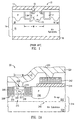
- An example of such a MOSFET is shown in Fig. 1, which shows a trench-gated MOSFET 10 including a gate 11, an N+ source region 12, a P-body 13, and a drain 14 which includes an N+ substrate 15 and an N-epitaxial layer 16.
- N+ source region is contacted by a metal layer 17 and drain 14 is contacted by a metal layer 18.
- a deep P+ diffusion 19 is formed in the center of the MOSFET cell.
- Deep P+ diffusion 19 is formed by implanting P-type dopant through the surface of the epitaxial layer 16 and heating the device to cause the dopant to diffuse downward to a level below the floor of the gate trench. The presence of the deep P+ diffusion causes the device to break down in the bulk silicon at the center of the MOSFET cell.
- the deep P+ diffusion does help to prevent hot carrier generation near the gate, it tends to limit the width W of the MOSFET cell and therefore the number of cells that can be formed within a given area of the chip. This in turn limits the on-resistance of the device, because the total cell perimeter available to conduct current generally increases with the cell density. Conversely, if W is made too small, an excessive amount of P-type dopant gets into the channel region 13A during the diffusion process, and this increases the threshold voltage of the device.
- a power MOSFET in accordance with this invention includes a semiconductor substrate of a first conductivity type and an epitaxial layer formed on a surface of the substrate, the epitaxial layer including a portion in contact with the substrate.
- the doping concentration of the portion of the epitaxial layer is lighter than the doping concentration of the substrate.
- a trench is formed at a surface of the epitaxial layer, the trench extending into the epitaxial layer and having a plurality of sections which define a MOSFET cell.
- a gate is formed in the trench.
- a source region of the first conductivity type is located adjacent a sidewall of the trench at a surface of the epitaxial layer in the MOSFET cell.
- a body of a second conductivity type adjoins the source region in the MOSFET cell, the body comprising a channel region adjacent the sidewall of the trench.
- a drain of the first conductivity type forms a first PN junction with the body, the body being located above the first PN junction, the drain being located below the first PN junction.
- the entire first PN junction is located at a level above a bottom of the trench, a portion of the first PN junction near the sidewall of the trench having a first breakdown voltage.
- a heavily-doped region of the second conductivity type is formed within the body at a central region of the MOSFET cell, the dopant concentration of the heavily-doped region being greater than the doping concentration of the body, such that a diode comprising a portion of a second PN junction at the central region of the MOSFET has a second breakdown voltage, the second breakdown voltage being lower than the first breakdown voltage.
- avalanche breakdown takes place at the central region of the MOSFET cell rather than near the sidewall of the trench where hot carriers could cause damage to the gate oxide layer.
- the lower boundary of the heavily-doped region preferably extends to a level that is below the bottom junction of the body region but above the bottom of the trench.
- Another aspect of the invention includes a method of fabricating a power MOSFET.
- the method comprises providing a semiconductor substrate of a first conductivity type; growing an epitaxial layer of the first conductivity on a surface of the substrate; forming a trench in the epitaxial layer, the trench defining a cell of the MOSFET; forming a first insulating layer on a surface of the trench; forming a gate in the trench, the gate being separated from the epitaxial layer by the insulating layer; implanting dopant of a second conductivity type into the epitaxial layer to form a body, a lower boundary of the body forming a first PN junction with a portion of the epitaxial layer of the first conductivity type; implanting dopant of the first conductivity type into the epitaxial layer to form a source region; depositing a second insulating layer over the epitaxial layer; forming an opening in the second insulating layer to expose at least a portion of the source region; implanting additional dopant of the second conductivity
- the thermal budget following the formation of the first insulating layer through the deposition of the metal layer is less than or equal to the equivalent of 950° C for 60 minutes. In another embodiment, the thermal budget following the formation of the first insulating layer through the deposition of the metal layer is less than or equal to the equivalent of 900° C for 50 minutes.
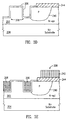
- FIG. 2A A cross-sectional view of a trench-gated power MOSFET in accordance with this invention is shown in Fig. 2A.
- MOSFET 20 is formed in an N-type epitaxial ("epi") layer 202, which is grown on an N+ substrate 204.
- a polysilicon gate 206 is located in a trench 208 and is isolated from the N-epi layer 202 by a gate oxide layer 210.
- a single MOSFET cell 212 is located between opposing segments of gate 206, it being understood that a typical power MOSFET would include a large number of MOSFET cells arrayed in a lattice-like arrangement.
- the individual cells could be closed geometric figures such as squares or hexagons or could be longitudinal stripes.
- the sections of the trench 208 define a mesa 209 which is typically from 1 ⁇ m to 4 ⁇ m wide. Trench 208 is typically from 0.7 ⁇ m to 1.6 ⁇ m deep.
- MOSFET cell 212 includes an N+ source region 216 and a P-body 218.
- N+ source region 216 is contacted by a metal layer 220 through openings in a borophosphosilicate glass (BPSG) layer 221.
- BPSG borophosphosilicate glass
- P-body 218 is contacted in a region outside the plane of the drawing.
- N+ source region 216 and P-body 218 are normally shorted together to prevent the parasitic bipolar transistor represented by drain region 214, P-body 218 and N+ source region 216 from becoming active.
- Termination region 240 also includes a P-region 246. As shown, field plate 242 is contacted by metal layer 220 through an opening in BPSG layer 221.
- P-body 218 includes a relatively heavily doped P+ region 222.
- P+ region 222 extends all the way to meet a substantially planar horizontal PN junction 217 between P-body 218 and N-epi layer 202.
- P+ region 222 extends downward to a level below PN junction 217 (as shown in Fig. 2C), but in most embodiments P+ region 218 does not extend to a level below the bottom of the trench 208.
- the lower extremity of P+ region may be at a level above PN junction.
- P+ region 222 is doped to a level such that a diode is formed in the center of MOSFET cell 212, the anode of the diode being represented by P+ region 222 and the cathode of the diode being represented by the N-epi layer 202.
- the central diode in MOSFET cell 212 has a breakdown voltage which is lower that the breakdown voltage of the PN junction 217 nearer the walls of the trench 208.
- avalanche breakdown occurs in MOSFET 20 at the center of MOSFET cell 212, at a location where damage to the gate oxide layer 210 is avoided.
- there is no deep diffusion in MOSFET cell 212 which limits the width W of MOSFET cell 212.
- Body region 218 is shown in detail in Fig. 2B. Because of the concentration of dopant in P+ region 222, the breakdown voltage of diode D1 at the center of MOSFET cell 212 is lower than the breakdown voltage of diode D2 near the wall of trench 208. Thus diode D1 breaks down before diode D2 and prevents the generation of hot carriers near trench 208 and gate oxide layer 210.
- Figs. 3A-3G illustrate the steps of a process for forming MOSFET 20.
- N-epi layer 202 on a surface of N+ substrate 204, as shown in Fig. 3A. This step is performed by a known process of epitaxial growth.
- N-epi layer 202 may be, for example 4 ⁇ m thick and may be doped with N-type impurity to a concentration of 3.5 x 10 16 cm -3 in the case of a 30V device.
- An oxide layer 302 is grown on the top surface of N-epi layer 202 and, by a known photolithographic process employing a first mask, a hole 304 is formed in oxide layer 302.
- a P-type impurity such as boron is implanted into N-epi layer 202 through hole 304 to form P region 246. This implant may be carried out, for example, at a dose of 1 x 10 14 cm -2 and an energy of 60 keV.
- P region 246 then driven-in at, for example, a temperature of 950° C for 180 minutes in a wet atmosphere. P region 246 diffuses both laterally and vertically as shown in Fig. 3B.
- a second photolithographic mask (not shown) is then formed, exposing what is to be the active area of the device, and oxide layer 244 is etched as shown in Fig. 3C.
- a third, trench mask 304 is then formed, with gaps 306 where the trench 208 is to be located, also as shown in Fig. 3C.
- the trench 208 is etched in N-epi layer 202 through mask 304, using a reactive ion etch (RIE) process.
- Trench 208 can be 0.8 ⁇ m wide and 0.9 ⁇ m deep, for example.
- a sacrificial oxide layer (not shown) can be grown on the exposed surfaces of N-epi layer 202 to repair the damage caused by the RIE etch.
- the sacrificial oxide layer is removed, and gate oxide layer 306 is grown to a thickness of, for example, 600 Angstroms on the exposed surfaces of N-epi layer 202, including in particular the sidewalls and floor of trench 208, as shown in Fig. 3D..
- Polysilicon layer 308 is then etched, leaving gate 206 and field plate 242, as shown in Fig. 3E.
- the top surface of gate 206 is roughly coplanar with the top surface of N-epi layer 202.
- P-body 218 is formed by implanting P-type impurity, for example boron, into N-epi layer 202. This is preferably accomplished using two implant steps: for example, the first at a dose of 6 x 10 12 cm -2 and an energy of 80 keV, and the second at a dose of 6 x 10 12 cm -2 and an energy of 150 keV. As shown in Fig. 3F, because the implantation goes into the entire region between the portions of trench 208, a PN junction 217 between P-body 218 and N-epi layer is substantially horizontal and planar.
- P-type impurity for example boron
- a fifth photolithographic mask (not shown) is formed, blocking the areas where the P-body is to be contacted in the third dimension with respect to the plane of Figs. 3A-3G.
- An N-type dopant such as arsenic is implanted, for example at a dose of 8 x 10 15 cm -2 and an energy of 80 keV, to form N+ source region 216.
- the fifth photolithographic mask is then removed.
- BPSG layer 221 is then deposited and allowed to flow at, for example, 875° C for 25 minutes.
- a sixth, contact mask (not shown) is formed on BPSG layer 221 with holes where contact will be made to N+ source region 216, field plate 242, and P-body 218.
- BPSG layer 221 and gate oxide layer 306 are etched through the holes in the sixth mask, forming an opening 310 to N+ source region, an opening 312 to field plate 242, and an opening (not shown) to P-body 218. Openings 310 and 312 are shown in dashed lines in Fig. 3G.
- a P-type impurity such as boron is then implanted through these openings to form P+ region 222.
- This can be done in a two-stage process, the first stage being performed at a dose of 1 x 10 15 cm -2 and an energy of 60 keV and the second stage being performed at a dose of 1 x 10 15 cm -2 and an energy of 120 keV.
- the first stage can be performed at a dose of 2 x 10 15 cm -2 and an energy of 60 keV and the second stage can be performed at a dose of 3 x 10 14 cm -2 and an energy of 120 keV, or the boron can be implanted in a one-stage process at a dose of 2 x 10 15 cm -2 and an energy of 100 keV. Because BPSG layer 221 overlaps the edges of N+ source region 216 near the sidewalls of trench 208, the P-type impurity is confined to a central region of the MOSFET cell 212.
- the energy of the implant can be adjusted to insure that the deepest portion of P+ region 222, coincides with the planar PN junction 217 between P-body region 218 and N-epi layer 202 (as shown in Figs. 2A and 2B), is located below the PN junction 217 (as shown in Fig. 2C), or is located above the PN junction (as shown in Fig. 2D).
- BPSG layer 221 is reflowed at, for example, 900° C for 30 minutes and metal layer 220, typically aluminum, is deposited to a thickness of, for example, 2.8 ⁇ m.
- metal mask is formed over the surface of metal layer 220, and metal layer 220 is etched in a conventional manner to form a source-body bus.
- MOSFET 20 shown in Figs. 2A-2D.
- the "thermal budget" of the process be limited such that P-body 218 does not diffuse appreciably but instead remains localized in the "mesa” between the sections of trench 208.
- the junction of P-body 218 and N-epi layer 202 should not move more than about 0.3 ⁇ m, and preferably not more than about 0.1 ⁇ m.
- the total "thermal budget" to which the structure is exposed following the implantation of P-body 218 should be limited to an amount that is less than or equal to the equivalent of 1050° C for 30 minutes and preferably less than 950° C for 60 minutes.
- the structure could be given a rapid thermal anneal (RTA) at about 1100° C for about 120 seconds. This thermal budget includes the heating required to flow and reflow BPSG layer 221, as described above.
- Figs. 4A and 4B show dopant profiles taken at a vertical cross-section of the mesa in a device fabricated in accordance with this invention.
- Fig. 4A shows the dopant profile immediately following the implantation of the P-body.
- Fig. 4B shows the dopant profile after the source has been implanted and both implanted dopants have been made electrically active during the BPSG flow and reflow anneals. Note the twin peaks in Fig. 4A from the two-stage implant. As indicated by a comparison of Figs.
- Figs. 4C and 4D show the dopant profiles in a conventional MOSFET after implantation of the P-body and in the finished device, respectively. Owing to the conventional diffusion of the body, the body-drain junction moved almost 1.0 ⁇ m deeper into the mesa, and the peak dopant concentration in the body was about 5 x 10 16 cm -3 .
- MOSFETs with different voltage ratings can be fabricated by varying the parameters of the process, in particular the thickness of N-epi layer 202 and gate oxide layer 210 and the doping concentration of P-body 218.
- Table 1 gives typical process parameters for 20V, 30V and 60V devices, including the gate oxide thickness T ox , the N-epi thickness T epi , the N-epi doping concentration N epi , and the implant dose and energy required to create the P-body and avoid punchthrough breakdown.
- the P-body is doped in a two-stage process to implant enough charge into the P-body region.
- the implant doses (D 1 ,D 2 ) and energies (E 1 ,E 2 ) for both of the stages is given.
- Rating T ox T epi N epi (cm -3 ) Dose 1 (cm -2 ) E 1 (keV)
- Dose 2 (cm -2 ) E 2 (keV) 20V 500A 3.5 ⁇ m 8E16 1E13 80 1E13 150 30V 600A 4 ⁇ m 3.5E16 6E12 80 6E12 150 60V 700A 5.5 ⁇ m 9E15 4E12 80 4E12 150
- a diode is formed at the center of the MOSFET cell. Dopant is implanted into the body to ensure that the central diode (D1) has an avalanche breakdown voltage lower than the avalanche breakdown voltage of the body-drain junction near the sidewall of the trench.
- the source contact opening in the BPSG layer is used for implanting the dopant but this need not be the case.
- Other masks or layers may be used to localize the dopant in the central area of the MOSFET cell.
- the breakdown voltage of diode D1 is a function of the doping concentration and gradient of P+ region 222 at its junction with N-epi layer 202 at the center of MOSFET cell 212.
- the breakdown voltage of diode D2 is a function of the doping concentration and gradient of the P-body 218 at its junction with N-epi layer 202 near gate trench 208 and includes the effects of the trench corners.
Landscapes
- Engineering & Computer Science (AREA)
- Microelectronics & Electronic Packaging (AREA)
- Power Engineering (AREA)
- Physics & Mathematics (AREA)
- Ceramic Engineering (AREA)
- Condensed Matter Physics & Semiconductors (AREA)
- General Physics & Mathematics (AREA)
- Computer Hardware Design (AREA)
- Manufacturing & Machinery (AREA)
- Metal-Oxide And Bipolar Metal-Oxide Semiconductor Integrated Circuits (AREA)
- Insulated Gate Type Field-Effect Transistor (AREA)
- Electrodes Of Semiconductors (AREA)
Priority Applications (1)
| Application Number | Priority Date | Filing Date | Title |
|---|---|---|---|
| EP08009037A EP1988579A3 (fr) | 1999-10-27 | 2000-01-19 | MOSFET de puissance à grille en tranchée |
Applications Claiming Priority (2)
| Application Number | Priority Date | Filing Date | Title |
|---|---|---|---|
| US428299 | 1995-04-25 | ||
| US09/428,299 US6348712B1 (en) | 1999-10-27 | 1999-10-27 | High density trench-gated power MOSFET |
Related Child Applications (1)
| Application Number | Title | Priority Date | Filing Date |
|---|---|---|---|
| EP08009037A Division EP1988579A3 (fr) | 1999-10-27 | 2000-01-19 | MOSFET de puissance à grille en tranchée |
Publications (2)
| Publication Number | Publication Date |
|---|---|
| EP1096574A2 true EP1096574A2 (fr) | 2001-05-02 |
| EP1096574A3 EP1096574A3 (fr) | 2003-03-12 |
Family
ID=23698310
Family Applications (2)
| Application Number | Title | Priority Date | Filing Date |
|---|---|---|---|
| EP08009037A Ceased EP1988579A3 (fr) | 1999-10-27 | 2000-01-19 | MOSFET de puissance à grille en tranchée |
| EP00300391A Ceased EP1096574A3 (fr) | 1999-10-27 | 2000-01-19 | MOSFET de puissance à grille en tranchée et méthode de fabrication correspondante |
Family Applications Before (1)
| Application Number | Title | Priority Date | Filing Date |
|---|---|---|---|
| EP08009037A Ceased EP1988579A3 (fr) | 1999-10-27 | 2000-01-19 | MOSFET de puissance à grille en tranchée |
Country Status (3)
| Country | Link |
|---|---|
| US (2) | US6348712B1 (fr) |
| EP (2) | EP1988579A3 (fr) |
| JP (1) | JP2001127292A (fr) |
Cited By (1)
| Publication number | Priority date | Publication date | Assignee | Title |
|---|---|---|---|---|
| US6309929B1 (en) * | 2000-09-22 | 2001-10-30 | Industrial Technology Research Institute And Genetal Semiconductor Of Taiwan, Ltd. | Method of forming trench MOS device and termination structure |
Families Citing this family (35)
| Publication number | Priority date | Publication date | Assignee | Title |
|---|---|---|---|---|
| US6472678B1 (en) * | 2000-06-16 | 2002-10-29 | General Semiconductor, Inc. | Trench MOSFET with double-diffused body profile |
| US7384854B2 (en) * | 2002-03-08 | 2008-06-10 | International Business Machines Corporation | Method of forming low capacitance ESD robust diodes |
| JP4209260B2 (ja) * | 2003-06-04 | 2009-01-14 | Necエレクトロニクス株式会社 | 半導体装置およびその製造方法 |
| JP4945055B2 (ja) * | 2003-08-04 | 2012-06-06 | ルネサスエレクトロニクス株式会社 | 半導体装置およびその製造方法 |
| KR100786488B1 (ko) * | 2004-01-10 | 2007-12-18 | 에이치브이브이아이 세미콘덕터즈, 인크. | 전력 반도체 장치 |
| WO2005084221A2 (fr) * | 2004-03-01 | 2005-09-15 | International Rectifier Corporation | Structure de contact auto-alignee pour dispositif a tranchees |
| US8530963B2 (en) * | 2005-01-06 | 2013-09-10 | Estivation Properties Llc | Power semiconductor device and method therefor |
| JP2006196545A (ja) * | 2005-01-11 | 2006-07-27 | Toshiba Corp | 半導体装置の製造方法 |
| US7655977B2 (en) * | 2005-10-18 | 2010-02-02 | International Rectifier Corporation | Trench IGBT for highly capacitive loads |
| EP1959495B1 (fr) * | 2005-11-22 | 2017-09-20 | Shindengen Electric Manufacturing Co., Ltd. | Dispositif semi-conducteur de puissance a grille en tranchee |
| US7667265B2 (en) * | 2006-01-30 | 2010-02-23 | Fairchild Semiconductor Corporation | Varying mesa dimensions in high cell density trench MOSFET |
| JP2006310836A (ja) * | 2006-04-05 | 2006-11-09 | Hvvi Semiconductors Inc | パワー半導体装置およびそのための方法 |
| JP2006310838A (ja) * | 2006-04-05 | 2006-11-09 | Hvvi Semiconductors Inc | パワー半導体装置およびそのための方法 |
| JP5073991B2 (ja) * | 2006-08-23 | 2012-11-14 | オンセミコンダクター・トレーディング・リミテッド | 絶縁ゲート型半導体装置 |
| US9437729B2 (en) * | 2007-01-08 | 2016-09-06 | Vishay-Siliconix | High-density power MOSFET with planarized metalization |
| JP2008244466A (ja) * | 2007-02-27 | 2008-10-09 | Matsushita Electric Ind Co Ltd | 半導体装置 |
| JP2008218711A (ja) * | 2007-03-05 | 2008-09-18 | Renesas Technology Corp | 半導体装置およびその製造方法、ならびに電源装置 |
| JP2007173878A (ja) * | 2007-03-28 | 2007-07-05 | Toshiba Corp | 半導体装置 |
| US9947770B2 (en) * | 2007-04-03 | 2018-04-17 | Vishay-Siliconix | Self-aligned trench MOSFET and method of manufacture |
| SE532625C2 (sv) * | 2007-04-11 | 2010-03-09 | Transic Ab | Halvledarkomponent i kiselkarbid |
| US9484451B2 (en) | 2007-10-05 | 2016-11-01 | Vishay-Siliconix | MOSFET active area and edge termination area charge balance |
| US20100171543A1 (en) * | 2009-01-08 | 2010-07-08 | Ciclon Semiconductor Device Corp. | Packaged power switching device |
| US20100237439A1 (en) * | 2009-03-18 | 2010-09-23 | Ming-Cheng Lee | High-voltage metal-dielectric-semiconductor device and method of the same |
| US9443974B2 (en) | 2009-08-27 | 2016-09-13 | Vishay-Siliconix | Super junction trench power MOSFET device fabrication |
| US9431530B2 (en) * | 2009-10-20 | 2016-08-30 | Vishay-Siliconix | Super-high density trench MOSFET |
| JP4791572B2 (ja) * | 2009-12-21 | 2011-10-12 | ルネサスエレクトロニクス株式会社 | 半導体装置 |
| US9842911B2 (en) | 2012-05-30 | 2017-12-12 | Vishay-Siliconix | Adaptive charge balanced edge termination |
| US9887259B2 (en) | 2014-06-23 | 2018-02-06 | Vishay-Siliconix | Modulated super junction power MOSFET devices |
| EP3183754A4 (fr) | 2014-08-19 | 2018-05-02 | Vishay-Siliconix | Transistor à effet de champ à semi-conducteur d'oxyde de métal à super jonction |
| CN107078161A (zh) | 2014-08-19 | 2017-08-18 | 维西埃-硅化物公司 | 电子电路 |
| US10522674B2 (en) | 2016-05-18 | 2019-12-31 | Rohm Co., Ltd. | Semiconductor with unified transistor structure and voltage regulator diode |
| US10692863B2 (en) | 2016-09-30 | 2020-06-23 | Rohm Co., Ltd. | Semiconductor device and semiconductor package |
| DE102017108738B4 (de) * | 2017-04-24 | 2022-01-27 | Infineon Technologies Ag | SiC-HALBLEITERVORRICHTUNG MIT EINEM VERSATZ IN EINEM GRABENBODEN UND HERSTELLUNGSVERFAHREN HIERFÜR |
| CN109256427A (zh) * | 2018-09-19 | 2019-01-22 | 电子科技大学 | 一种集成肖特基二极管的SiC MOSFET器件 |
| TWI739252B (zh) * | 2019-12-25 | 2021-09-11 | 杰力科技股份有限公司 | 溝槽式mosfet元件及其製造方法 |
Citations (1)
| Publication number | Priority date | Publication date | Assignee | Title |
|---|---|---|---|---|
| US5877538A (en) * | 1995-06-02 | 1999-03-02 | Silixonix Incorporated | Bidirectional trench gated power MOSFET with submerged body bus extending underneath gate trench |
Family Cites Families (10)
| Publication number | Priority date | Publication date | Assignee | Title |
|---|---|---|---|---|
| US5072266A (en) * | 1988-12-27 | 1991-12-10 | Siliconix Incorporated | Trench DMOS power transistor with field-shaping body profile and three-dimensional geometry |
| JPH0493084A (ja) * | 1990-08-08 | 1992-03-25 | Matsushita Electron Corp | 半導体装置およびその製造方法 |
| GB9216599D0 (en) | 1992-08-05 | 1992-09-16 | Philips Electronics Uk Ltd | A semiconductor device comprising a vertical insulated gate field effect device and a method of manufacturing such a device |
| US5410170A (en) * | 1993-04-14 | 1995-04-25 | Siliconix Incorporated | DMOS power transistors with reduced number of contacts using integrated body-source connections |
| US6049108A (en) * | 1995-06-02 | 2000-04-11 | Siliconix Incorporated | Trench-gated MOSFET with bidirectional voltage clamping |
| US5689128A (en) * | 1995-08-21 | 1997-11-18 | Siliconix Incorporated | High density trenched DMOS transistor |
| US5629543A (en) * | 1995-08-21 | 1997-05-13 | Siliconix Incorporated | Trenched DMOS transistor with buried layer for reduced on-resistance and ruggedness |
| DE69530517T2 (de) * | 1995-11-02 | 2003-12-24 | Nat Semiconductor Corp | Halbleiteranordnung mit isoliertem gate mit implantaten für verbesserte robustheit |
| US6429481B1 (en) * | 1997-11-14 | 2002-08-06 | Fairchild Semiconductor Corporation | Field effect transistor and method of its manufacture |
| US6285060B1 (en) * | 1999-12-30 | 2001-09-04 | Siliconix Incorporated | Barrier accumulation-mode MOSFET |
-
1999
- 1999-10-27 US US09/428,299 patent/US6348712B1/en not_active Expired - Lifetime
-
2000
- 2000-01-19 EP EP08009037A patent/EP1988579A3/fr not_active Ceased
- 2000-01-19 EP EP00300391A patent/EP1096574A3/fr not_active Ceased
- 2000-01-26 JP JP2000016475A patent/JP2001127292A/ja active Pending
-
2001
- 2001-03-21 US US09/816,717 patent/US6534366B2/en not_active Expired - Lifetime
Patent Citations (1)
| Publication number | Priority date | Publication date | Assignee | Title |
|---|---|---|---|---|
| US5877538A (en) * | 1995-06-02 | 1999-03-02 | Silixonix Incorporated | Bidirectional trench gated power MOSFET with submerged body bus extending underneath gate trench |
Cited By (1)
| Publication number | Priority date | Publication date | Assignee | Title |
|---|---|---|---|---|
| US6309929B1 (en) * | 2000-09-22 | 2001-10-30 | Industrial Technology Research Institute And Genetal Semiconductor Of Taiwan, Ltd. | Method of forming trench MOS device and termination structure |
Also Published As
| Publication number | Publication date |
|---|---|
| EP1096574A3 (fr) | 2003-03-12 |
| JP2001127292A (ja) | 2001-05-11 |
| EP1988579A2 (fr) | 2008-11-05 |
| US6348712B1 (en) | 2002-02-19 |
| US6534366B2 (en) | 2003-03-18 |
| EP1988579A3 (fr) | 2008-11-19 |
| US20010045598A1 (en) | 2001-11-29 |
Similar Documents
| Publication | Publication Date | Title |
|---|---|---|
| US6534366B2 (en) | Method of fabricating trench-gated power MOSFET | |
| US10763351B2 (en) | Vertical trench DMOSFET having integrated implants forming enhancement diodes in parallel with the body diode | |
| US7148111B2 (en) | Method of manufacturing a trench transistor having a heavy body region | |
| US6764906B2 (en) | Method for making trench mosfet having implanted drain-drift region | |
| US7795675B2 (en) | Termination for trench MIS device | |
| US5814858A (en) | Vertical power MOSFET having reduced sensitivity to variations in thickness of epitaxial layer | |
| US6600193B2 (en) | Trench MOSFET having implanted drain-drift region | |
| US7435650B2 (en) | Process for manufacturing trench MIS device having implanted drain-drift region and thick bottom oxide | |
| EP2068364A2 (fr) | Transistor MOS à tranchée comportant une electrode source noyée | |
| US7161208B2 (en) | Trench mosfet with field relief feature | |
| US20090283823A1 (en) | Semiconductor device and method of manufacturing semiconductor device | |
| US20060038223A1 (en) | Trench MOSFET having drain-drift region comprising stack of implanted regions | |
| US6492679B1 (en) | Method for manufacturing a high voltage MOSFET device with reduced on-resistance |
Legal Events
| Date | Code | Title | Description |
|---|---|---|---|
| PUAI | Public reference made under article 153(3) epc to a published international application that has entered the european phase |
Free format text: ORIGINAL CODE: 0009012 |
|
| AK | Designated contracting states |
Kind code of ref document: A2 Designated state(s): AT BE CH CY DE DK ES FI FR GB GR IE IT LI LU MC NL PT SE |
|
| AX | Request for extension of the european patent |
Free format text: AL;LT;LV;MK;RO;SI |
|
| 17P | Request for examination filed |
Effective date: 20011114 |
|
| PUAL | Search report despatched |
Free format text: ORIGINAL CODE: 0009013 |
|
| AK | Designated contracting states |
Kind code of ref document: A3 Designated state(s): AT BE CH CY DE DK ES FI FR GB GR IE IT LI LU MC NL PT SE Designated state(s): AT BE CH CY DE DK ES FI FR GB GR IE IT LI LU MC NL PT SE |
|
| AX | Request for extension of the european patent |
Extension state: AL LT LV MK RO SI |
|
| AKX | Designation fees paid |
Designated state(s): DE FR GB IT NL |
|
| 17Q | First examination report despatched |
Effective date: 20031114 |
|
| 17Q | First examination report despatched |
Effective date: 20031114 |
|
| APBK | Appeal reference recorded |
Free format text: ORIGINAL CODE: EPIDOSNREFNE |
|
| APBN | Date of receipt of notice of appeal recorded |
Free format text: ORIGINAL CODE: EPIDOSNNOA2E |
|
| APBR | Date of receipt of statement of grounds of appeal recorded |
Free format text: ORIGINAL CODE: EPIDOSNNOA3E |
|
| APAF | Appeal reference modified |
Free format text: ORIGINAL CODE: EPIDOSCREFNE |
|
| APAK | Date of receipt of statement of grounds of an appeal modified |
Free format text: ORIGINAL CODE: EPIDOSCNOA3E |
|
| APBT | Appeal procedure closed |
Free format text: ORIGINAL CODE: EPIDOSNNOA9E |
|
| STAA | Information on the status of an ep patent application or granted ep patent |
Free format text: STATUS: THE APPLICATION HAS BEEN REFUSED |
|
| 18R | Application refused |
Effective date: 20120320 |