EP1090335B1 - System and method for controlling the manufacture of discrete parts in semiconductor fabrication using model predictive control - Google Patents
System and method for controlling the manufacture of discrete parts in semiconductor fabrication using model predictive control Download PDFInfo
- Publication number
- EP1090335B1 EP1090335B1 EP98964806A EP98964806A EP1090335B1 EP 1090335 B1 EP1090335 B1 EP 1090335B1 EP 98964806 A EP98964806 A EP 98964806A EP 98964806 A EP98964806 A EP 98964806A EP 1090335 B1 EP1090335 B1 EP 1090335B1
- Authority
- EP
- European Patent Office
- Prior art keywords
- tool
- run
- input
- output
- process state
- Prior art date
- Legal status (The legal status is an assumption and is not a legal conclusion. Google has not performed a legal analysis and makes no representation as to the accuracy of the status listed.)
- Expired - Lifetime
Links
Images

Classifications
-
- G—PHYSICS
- G05—CONTROLLING; REGULATING
- G05B—CONTROL OR REGULATING SYSTEMS IN GENERAL; FUNCTIONAL ELEMENTS OF SUCH SYSTEMS; MONITORING OR TESTING ARRANGEMENTS FOR SUCH SYSTEMS OR ELEMENTS
- G05B19/00—Program-control systems
- G05B19/02—Program-control systems electric
- G05B19/418—Total factory control, i.e. centrally controlling a plurality of machines, e.g. direct or distributed numerical control [DNC], flexible manufacturing systems [FMS], integrated manufacturing systems [IMS] or computer integrated manufacturing [CIM]
-
- H—ELECTRICITY
- H10—SEMICONDUCTOR DEVICES; ELECTRIC SOLID-STATE DEVICES NOT OTHERWISE PROVIDED FOR
- H10P—GENERIC PROCESSES OR APPARATUS FOR THE MANUFACTURE OR TREATMENT OF DEVICES COVERED BY CLASS H10
- H10P74/00—Testing or measuring during manufacture or treatment of wafers, substrates or devices
- H10P74/23—Testing or measuring during manufacture or treatment of wafers, substrates or devices characterised by multiple measurements, corrections, marking or sorting processes
-
- G—PHYSICS
- G05—CONTROLLING; REGULATING
- G05B—CONTROL OR REGULATING SYSTEMS IN GENERAL; FUNCTIONAL ELEMENTS OF SUCH SYSTEMS; MONITORING OR TESTING ARRANGEMENTS FOR SUCH SYSTEMS OR ELEMENTS
- G05B19/00—Program-control systems
- G05B19/02—Program-control systems electric
- G05B19/418—Total factory control, i.e. centrally controlling a plurality of machines, e.g. direct or distributed numerical control [DNC], flexible manufacturing systems [FMS], integrated manufacturing systems [IMS] or computer integrated manufacturing [CIM]
- G05B19/41885—Total factory control, i.e. centrally controlling a plurality of machines, e.g. direct or distributed numerical control [DNC], flexible manufacturing systems [FMS], integrated manufacturing systems [IMS] or computer integrated manufacturing [CIM] characterised by modeling, simulation of the manufacturing system
-
- Y—GENERAL TAGGING OF NEW TECHNOLOGICAL DEVELOPMENTS; GENERAL TAGGING OF CROSS-SECTIONAL TECHNOLOGIES SPANNING OVER SEVERAL SECTIONS OF THE IPC; TECHNICAL SUBJECTS COVERED BY FORMER USPC CROSS-REFERENCE ART COLLECTIONS [XRACs] AND DIGESTS
- Y02—TECHNOLOGIES OR APPLICATIONS FOR MITIGATION OR ADAPTATION AGAINST CLIMATE CHANGE
- Y02P—CLIMATE CHANGE MITIGATION TECHNOLOGIES IN THE PRODUCTION OR PROCESSING OF GOODS
- Y02P90/00—Enabling technologies with a potential contribution to greenhouse gas [GHG] emissions mitigation
- Y02P90/02—Total factory control, e.g. smart factories, flexible manufacturing systems [FMS] or integrated manufacturing systems [IMS]
Definitions
- the present invention relates generally to the manufacture of discrete parts using model predictive control, more specifically, to a system and method for controlling the manufacture of semiconductor wafers using model predictive control.
- Semiconductor fabrication includes the fabrication of discrete parts, such as runs or batches of wafers, each of which includes one or more wafers fabricated using similar processing.
- One challenge in semiconductor fabrication is controlling equipment inputs from run to run.
- the challenge in run-to-run control stems from a lack of real-time information about process states and output states while processing a given wafer or group of wafers and variable input states of incoming wafers.
- Chemical-mechanical polishing is a common and rapidly growing process used in the fabrication of semiconductor wafers for planarizing silicon dioxide as well as other types of layers on semiconductor wafers.
- Chemical mechanical polishing typically utilizes an abrasive slurry disbursed in an alkaline or acidic solution to planarize the surface of the wafer through a combination of mechanical and chemical action.
- a typical chemical mechanical polishing tool includes a rotatable circular platen or table on which a polishing pad is mounted and a polishing device is positioned above the pad.
- the polishing device includes one or more rotating carrier heads to which wafers can be secured typically through the use of vacuum pressure. In use, the platen is rotated and an abrasive slurry is disbursed onto the polishing pad.
- a downforce is applied to each rotating carrier head to press its wafer against the polishing pad.
- the surface of the wafer is mechanically and chemically polished.
- the usual adjustment parameter or tool input is polishing time (though in some operations, carrier downforce is input as well).
- Other parameters, such as table speed and carrier downforces are fixed for the process.
- tool outputs such as post-polish thicknesses of polished layers
- variations in post-polish thicknesses can, for example, significantly degrade subsequent processing steps, such as lithography.
- y k is the output at batch k
- B is the process gain
- k-1 is the input at batch k calculated from information up through batch k-1
- k-1 is the estimate for the intercept
- e k is unknown process noise entering the system.
- the system gain and the initial value of the intercept is modeled a priori from designed experiments.
- the intercept is typically updated recursively by an observer of the form: where ⁇ is the exponential weighting factor, or tuning parameter, of the observer.
- the weighting factor ⁇ takes a value between 0 and 1 and is chosen based on the desired properties of the observer.
- the input for batch k (u k
- k-1 (T-c k
- PCC predictor-corrector controllers
- k- 1 y * (y k -B * u k
- k-1 is the smoothed trend of the intercept.
- EP-A-0,643,344 discloses a run-by-run process control system in which machine settings for a given process (such as polish time in a CMP process) are selected by a controller based on a series of model outputs from a predictive process model, the model outputs representing equations that describe the process behaviour. The controller then adjusts these model outputs in accordance with the output obtained from the machine being run.
- machine settings for a given process such as polish time in a CMP process
- US-A-5,595,601 discloses a CMP method for planariang a semiconductor surface. The thickness of a film which has been polished is measured, and a polishing time for the next wafer is calculated based on the measured thickness.
- US-A-5,655,951 discloses a method for selectively reconditioning a planarizimg surface of a polishing pad used in a CMP process.
- a desired polishing rate is selected based on a set of parameters for a particular substrate, and the desired change in pad thickness is then estimated for reconditioning the pad to achieve the desired polishing rate.
- a layer of material is then removed from the planarizing surface having a thickness approximately equal to the desired change in pad thickness.
- the present invention provides a system and method for controlling the manufacture of semiconductor wafers using model predictive control.
- a tool output of the manufacturing tool is determined based on a first wafer run.
- a tool input for a subsequent wafer run is determined by minimizing an optimization equation being dependent upon a model which relates tool output to tool process state and tool process state to tool input and previous tool process state.
- the tool input is then provided to the manufacturing tool for processing a second wafer run. In this manner, processing by the tool or tool age is taken into account in determining the tool input for a subsequent run. This can reduce variations in tool output from run-to-run and improve the characteristics of the ultimately formed semiconductor devices.
- the tool may, for example, be a chemical mechanical polishing tool with the tool input being polishing time and the tool output being a post-polish wafer layer thickness associated with CMP tool for a run.
- the present invention generally provides a system and method for run-to-run control of the manufacture of semiconductor wafers using model predictive control.
- the invention is particularly suited for controlling post-polish thicknesses of wafer layers, such as dielectric layers, by chemical mechanical polishing (CMP) tools.
- CMP chemical mechanical polishing
- FIG. 1 illustrates, by way of example, a polishing tool which may be used with the present invention.
- the exemplary polishing tool 100 generally includes a polishing pad 110 mounted on a platen 112 and a multi-head carrier 120 positioned above the polishing pad 110.
- the multi-head carrier 120 typically includes a plurality of rotatable polishing arms 122, each of which includes a head 124. Wafers can be secured to the carrier heads 124 by known techniques such as vacuum pressure.
- a source of polishing fluid (not shown) is also provided to supply polishing fluid to the pad 110 for polishing. It should be appreciated that the polishing tool 100 is illustrated by way of example only. Other polishing tools having one or more polishing arms may be used with the present invention.
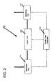
- FIG. 2 illustrates an exemplary control system for controlling a polishing tool, such as the one described above, in accordance with one embodiment of the invention.
- the exemplary control system 200 includes two metrology tools 210 and 212 for measuring pre-polish thicknesses and post-polish thicknesses of wafer layers (e.g., dielectric layers), respectively. It should be appreciated that while two metrology tools are illustrated, a single metrology tool may be used to perform both pre- and post-polish thickness measurements.
- the two metrology tools 210 and 212 are coupled to a polish tool 220.
- a suitable metrology tool for many applications is the Optiprobe metrology tool by Thermawave.
- the system further includes a controller 230 coupled to the polishing tool 220 for controlling the inputs, such as polishing time to the polishing tool 220.
- the controller 230 generally receives pre- and post-polish thickness measurements from the metrology tools 210 and 212 for a wafer run and uses the thickness measurements to control a polishing time input to the polish tool 220 for a subsequent wafer run.
- the polishing time input may, for example, be a deviation from a nominal polishing time.
- the controller may, for example, be a model predictive controller implemented using, for example, MatLab Optimization Toolbox® routines.
- the controller 230 may be interfaced with the polish tool 220 using, for example, an Advance Process Control Framework interface.
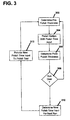
- a first wafer group (e.g., one or more wafers depending on the number of polishing arms) is provided to the metrology tool 210 for measuring a pre-polish thickness of each wafer layer to be polished.
- Each pre-polish thickness is then stored, typically in a database accessible by the controller 230.
- the wafer group is then loaded onto the carrier head(s) of the tool's polishing arm(s) and the wafer group is polished using a predetermined polishing time to remove at least part of the wafer layer of each wafer, as indicated at block 304.
- the polishing time may be either calculated by the controller 230 at block 310 (as will be discussed below) or, for an initial run, predefined by an operator.
- the polishing is typically performed at a predetermined table speed with predetermined downforces on each arm.
- the controller 230 may, however, be used to determine the downforces on each arm if desired.
- Techniques for controlling the downforces on the polishing arms of a multi-arm polishing tool are described in the co-pending and commonly assigned U.S. patent application, entitled “SYSTEM AND METHOD FOR CONTROLLING A MULTI-ARM POLISHING TOOL,” having an Attorney Docket No. 11729.219US01, the contents of which are herein incorporated by reference.
- the post-polish thickness of the polished layer of each wafer are determined by metrology tool 212, as indicated at block 306.
- the post-polish thickness for each wafer is typically stored in the database accessible by the controller 230.
- the controller 230 determines whether the wafer run has finished. If not, control moves to block 302 and another wafer group is polished using the same polishing time input. If the run has finished, control moves to block 310 where a new polishing time input (which will be applied to a subsequent wafer run) is determined by the controller 230.
- the controller 230 determines the new polishing time input for the polishing tool 220 by solving an optimization equation based on a model which includes a predetermined relationship between predicted removal amount and current removal amount.
- the new polishing time input is determined by solving an optimization equation based on a process model.
- a z k advantageously takes process dynamics, such as tool drift resulting from pad degradation, into account and allows the polishing time input to be determined based on such process dynamics.
- the fixed coefficient a may be view as a memory effect coefficient which takes into account the effects of one polish process on future polish processes.
- a and b can vary depending on the type of polishing tool, the table speed, the arm downforces, the slurry and the topography of the wafer being polished.
- the coefficients a and b and noise w k are determined experimentally for a given polishing tool using test wafers. Suitable experimental techniques include well-known design of experiment (DOE) or pseudo-random binary sequence system identification techniques.
- DOE design of experiment
- b range from 40 to 250 Angstroms/second.
- the noise w k is typically a random variable normally distributed, e.g., at about 5-10% of target output thickness.
- the exemplary process model may further include a feed forward model which accounts for upstream variations in a process, such as pre-polish layer thicknesses between runs.
- a feed forward model which accounts for upstream variations in a process, such as pre-polish layer thicknesses between runs.
- the deposition and polishing steps are not tightly coupled and a polishing tool typically receives wafers from several different deposition tools.
- the pre-polish thickness of wafers typically (and often, substantially) varies from run-to-run.
- the incoming thickness level f k is an average of the incoming thickness of the wafer(s) processed at run k.
- the factor ⁇ accounts for drift in the upstream process (e.g., drift in a deposition tool). For many applications ⁇ may equal 1 (one), signifying that the best estimate of the next incoming thickness f k+1 is the last incoming thickness f k .
- ⁇ may equal 1 (one), signifying that the best estimate of the next incoming thickness f k+1 is the last incoming thickness f k .
- the exemplary process model may further include an unknown state disturbance model which accounts for unknown state disturbances, such as slurry changes, pad changes, etc., between runs.
- the value d k may also be filtered if desired.
- the factor ⁇ may be used to account for drift in the unknown disturbance. For many applications ⁇ may equal 1 (one), signifying that the best estimate of the next incoming unknown disturbance d k+1 is the last unknown disturbance d k .
- the use of such an unknown disturbance model can further enhance controller performance.
- the output model may modified to account for time delay in the feedback of the metrology tools by virtue of the time needed to measure layer thicknesses.
- One suitable output model includes a time delay of 2 units (i.e., 2 runs) and is as follows.
- An exemplary optimization equation for controller may be: subject to Equations [10] and [11] above.
- y T is a target output
- Q is the weight on the output error (the difference between post-polish thickness at run k+j+1 and target post-polish thickness y T )
- S is the weight on the rate of change of the inputs ⁇ u k+j
- R is the weight on the inputs u k+j
- u N is the sequence of N input moves computed as the solution to equation [3].
- N is suitably selected based on the number of runs which the controller is desired to look ahead when computing a solution at run k.
- the controller may be simplified by using a sequence of future moves N of one (1).
- the optimization equation reduces to: subject to Equations [10] and [11] above.
- the weights Q, R (if appropriate) and S may be suitably selected based on the desired weighting of the respective functions (i.e., the output errors, the inputs, and the rate of change of the inputs). This allows control of the polish tool to be tuned for a desired performance. For example, performance such as minimizing output deviations from target or minimizing changes in polishing time can be tuned by varying weights Q and S.
- the optimization equation (e.g., equation 13 or 14 above) of the controller 230 may be solved for the input, polishing time u k , which minimizes the optimization equation over a predetermined sequence of inputs N.
- the optimization equation may further be solved for the polishing time which minimizes the optimization equation (e.g., equation 13 or 14 above) over N future runs taking into account constraints on the polishing tool.
- the constraints are typically dictated by processing considerations and may include, for example, requiring polishing time input to be less than a certain value (e.g., u k ⁇ time max ) or that change in polishing time inputs between runs must lie between an upper bound and a lower bound (e.g., B L ⁇ u k+1 -u k ⁇ B U ).
- the controller 230 determines a post-polish thickness level y k , and a pre-polish thickness level f k for the tool for the current run (run k).
- the pre-polish and post-polish thicknesses f k and y k of the tool may be the averaged pre- and post-polish thickness for the wafer(s) polished during run k.
- d k for the tool is also determined.
- the value d k for the tool at run k may be the difference between an expected post-polishing thickness for run k and the measured post-polish thickness level at run k.
- the controller 230 uses the measured pre- and post-polish thickness levels f k and y k (and, in desired cases, the unknown disturbance, d k ), the controller 230 then solves an optimization equation (e.g., equation 13 or 14 above) for a new polishing time u k (to be applied during the next run, run k+1) which minimizes the optimization equation subject to any constraints over the predetermined future inputs N.
- an optimization equation e.g., equation 13 or 14 above
- run-to-run variations in post polish thickness can be reduced as compared to conventional control techniques (such as EWMA or PCC techniques).
- the above control system reduces such run-to-run variations by, for example, taking into account drift of the process in determining future process output and inputs. In particular a fixed amount of drift ( a in equation [7]) is incorporated into the controller for more accurately controlling the polishing tool. Further reductions in run-to-run variations may be provided by incorporating measured feed forward disturbance (e.g., thickness disturbance) and unknown disturbance models into the process model and controller's optimization equation.
- polishing tools such as CMP tools
- the present invention is not limited to the control of polishing tools, but extends to cover any manufacturing tool used in run-to-run manufacturing.
- Other systems or tools, to which the present invention is applicable include, for example, deposition tools, such as chemical-vapor deposition (CVD) tools and sputter deposition tools.
- CVD deposition tools the tool output may be deposition layer thickness, while the process state may be chamber cleanliness.
- sputter deposition tools the tool output may be deposition layer thickness, while the process state may be target age or cleanliness.
Landscapes
- Engineering & Computer Science (AREA)
- Manufacturing & Machinery (AREA)
- General Engineering & Computer Science (AREA)
- Quality & Reliability (AREA)
- Physics & Mathematics (AREA)
- General Physics & Mathematics (AREA)
- Automation & Control Theory (AREA)
- Mechanical Treatment Of Semiconductor (AREA)
- Constituent Portions Of Griding Lathes, Driving, Sensing And Control (AREA)
- General Factory Administration (AREA)
- Cleaning Or Drying Semiconductors (AREA)
Applications Claiming Priority (3)
| Application Number | Priority Date | Filing Date | Title |
|---|---|---|---|
| US09/105,979 US6230069B1 (en) | 1998-06-26 | 1998-06-26 | System and method for controlling the manufacture of discrete parts in semiconductor fabrication using model predictive control |
| US105979 | 1998-06-26 | ||
| PCT/US1998/027074 WO2000000874A1 (en) | 1998-06-26 | 1998-12-18 | System and method for controlling the manufacture of discrete parts in semiconductor fabrication using model predictive control |
Publications (2)
| Publication Number | Publication Date |
|---|---|
| EP1090335A1 EP1090335A1 (en) | 2001-04-11 |
| EP1090335B1 true EP1090335B1 (en) | 2003-02-26 |
Family
ID=22308814
Family Applications (1)
| Application Number | Title | Priority Date | Filing Date |
|---|---|---|---|
| EP98964806A Expired - Lifetime EP1090335B1 (en) | 1998-06-26 | 1998-12-18 | System and method for controlling the manufacture of discrete parts in semiconductor fabrication using model predictive control |
Country Status (6)
| Country | Link |
|---|---|
| US (1) | US6230069B1 (https=) |
| EP (1) | EP1090335B1 (https=) |
| JP (2) | JP4297614B2 (https=) |
| KR (1) | KR100572039B1 (https=) |
| DE (1) | DE69811742T2 (https=) |
| WO (1) | WO2000000874A1 (https=) |
Families Citing this family (100)
| Publication number | Priority date | Publication date | Assignee | Title |
|---|---|---|---|---|
| US6169931B1 (en) * | 1998-07-29 | 2001-01-02 | Southwest Research Institute | Method and system for modeling, predicting and optimizing chemical mechanical polishing pad wear and extending pad life |
| JP3897922B2 (ja) * | 1998-12-15 | 2007-03-28 | 株式会社東芝 | 半導体装置の製造方法、及びコンピュ−タ読取り可能な記録媒体 |
| US7069101B1 (en) * | 1999-07-29 | 2006-06-27 | Applied Materials, Inc. | Computer integrated manufacturing techniques |
| US6546306B1 (en) * | 1999-08-11 | 2003-04-08 | Advanced Micro Devices, Inc. | Method for adjusting incoming film thickness uniformity such that variations across the film after polishing minimized |
| US6492273B1 (en) | 1999-08-31 | 2002-12-10 | Micron Technology, Inc. | Methods and apparatuses for monitoring and controlling mechanical or chemical-mechanical planarization of microelectronic substrate assemblies |
| US6560503B1 (en) * | 1999-10-05 | 2003-05-06 | Advanced Micro Devices, Inc. | Method and apparatus for monitoring controller performance using statistical process control |
| US7461040B1 (en) | 1999-10-31 | 2008-12-02 | Insyst Ltd. | Strategic method for process control |
| IL159332A0 (en) | 1999-10-31 | 2004-06-01 | Insyst Ltd | A knowledge-engineering protocol-suite |
| US6820070B2 (en) | 2000-06-07 | 2004-11-16 | Insyst Ltd. | Method and tool for data mining in automatic decision making systems |
| US6640151B1 (en) * | 1999-12-22 | 2003-10-28 | Applied Materials, Inc. | Multi-tool control system, method and medium |
| AU2001249724A1 (en) * | 2000-04-03 | 2001-10-15 | Speed-Fam-Ipec Corporation | System and method for predicting software models using material-centric process instrumentation |
| GB0008908D0 (en) | 2000-04-11 | 2000-05-31 | Hewlett Packard Co | Shopping assistance service |
| US6741903B1 (en) | 2000-06-01 | 2004-05-25 | Adavanced Micro Devices, Inc. | Method for relating photolithography overlay target damage and chemical mechanical planarization (CMP) fault detection to CMP tool indentification |
| US6556884B1 (en) | 2000-06-16 | 2003-04-29 | Advanced Micro Devices, Inc. | Method and apparatus for interfacing a statistical process control system with a manufacturing process control framework |
| US6512991B1 (en) * | 2000-07-12 | 2003-01-28 | Advanced Micro Devices, Inc. | Method and apparatus for reducing deposition variation by modeling post-clean chamber performance |
| US6567718B1 (en) * | 2000-07-28 | 2003-05-20 | Advanced Micro Devices, Inc. | Method and apparatus for monitoring consumable performance |
| US6708074B1 (en) | 2000-08-11 | 2004-03-16 | Applied Materials, Inc. | Generic interface builder |
| US6625513B1 (en) * | 2000-08-15 | 2003-09-23 | Applied Materials, Inc. | Run-to-run control over semiconductor processing tool based upon mirror image target |
| US6919957B2 (en) | 2000-09-20 | 2005-07-19 | Kla-Tencor Technologies Corp. | Methods and systems for determining a critical dimension, a presence of defects, and a thin film characteristic of a specimen |
| US7349090B2 (en) | 2000-09-20 | 2008-03-25 | Kla-Tencor Technologies Corp. | Methods and systems for determining a property of a specimen prior to, during, or subsequent to lithography |
| US7106425B1 (en) | 2000-09-20 | 2006-09-12 | Kla-Tencor Technologies Corp. | Methods and systems for determining a presence of defects and a thin film characteristic of a specimen |
| US6891627B1 (en) | 2000-09-20 | 2005-05-10 | Kla-Tencor Technologies Corp. | Methods and systems for determining a critical dimension and overlay of a specimen |
| US6633831B2 (en) | 2000-09-20 | 2003-10-14 | Kla Tencor Technologies | Methods and systems for determining a critical dimension and a thin film characteristic of a specimen |
| US7130029B2 (en) | 2000-09-20 | 2006-10-31 | Kla-Tencor Technologies Corp. | Methods and systems for determining an adhesion characteristic and a thickness of a specimen |
| US6766283B1 (en) | 2000-10-13 | 2004-07-20 | Insyst Ltd. | System and method for monitoring process quality control |
| JP4827292B2 (ja) * | 2000-11-01 | 2011-11-30 | アプライド マテリアルズ インコーポレイテッド | 研磨装置 |
| US7188142B2 (en) | 2000-11-30 | 2007-03-06 | Applied Materials, Inc. | Dynamic subject information generation in message services of distributed object systems in a semiconductor assembly line facility |
| US7092863B2 (en) | 2000-12-26 | 2006-08-15 | Insyst Ltd. | Model predictive control (MPC) system using DOE based model |
| US6728587B2 (en) * | 2000-12-27 | 2004-04-27 | Insyst Ltd. | Method for global automated process control |
| US7123978B2 (en) * | 2000-12-27 | 2006-10-17 | Insyst Ltd. | Method for dynamically targeting a batch process |
| US6538730B2 (en) | 2001-04-06 | 2003-03-25 | Kla-Tencor Technologies Corporation | Defect detection system |
| EP1249864A1 (de) * | 2001-04-09 | 2002-10-16 | ABB Schweiz AG | Verfahren und Gerät zum Reduzieren der Dicke von dünnen Scheiben |
| WO2002103776A2 (en) * | 2001-06-18 | 2002-12-27 | Advanced Micro Devices, Inc. | Method for relating photolithography overlay target damage and chemical mechanical planarization (cmp) fault detection to cmp tool identification |
| US7160739B2 (en) | 2001-06-19 | 2007-01-09 | Applied Materials, Inc. | Feedback control of a chemical mechanical polishing device providing manipulation of removal rate profiles |
| US7201936B2 (en) | 2001-06-19 | 2007-04-10 | Applied Materials, Inc. | Method of feedback control of sub-atmospheric chemical vapor deposition processes |
| US6910947B2 (en) * | 2001-06-19 | 2005-06-28 | Applied Materials, Inc. | Control of chemical mechanical polishing pad conditioner directional velocity to improve pad life |
| US7101799B2 (en) | 2001-06-19 | 2006-09-05 | Applied Materials, Inc. | Feedforward and feedback control for conditioning of chemical mechanical polishing pad |
| US20020192966A1 (en) * | 2001-06-19 | 2002-12-19 | Shanmugasundram Arulkumar P. | In situ sensor based control of semiconductor processing procedure |
| US7047099B2 (en) * | 2001-06-19 | 2006-05-16 | Applied Materials Inc. | Integrating tool, module, and fab level control |
| US7698012B2 (en) | 2001-06-19 | 2010-04-13 | Applied Materials, Inc. | Dynamic metrology schemes and sampling schemes for advanced process control in semiconductor processing |
| US6913938B2 (en) | 2001-06-19 | 2005-07-05 | Applied Materials, Inc. | Feedback control of plasma-enhanced chemical vapor deposition processes |
| US7082345B2 (en) * | 2001-06-19 | 2006-07-25 | Applied Materials, Inc. | Method, system and medium for process control for the matching of tools, chambers and/or other semiconductor-related entities |
| US7337019B2 (en) * | 2001-07-16 | 2008-02-26 | Applied Materials, Inc. | Integration of fault detection with run-to-run control |
| US6863771B2 (en) * | 2001-07-25 | 2005-03-08 | Micron Technology, Inc. | Differential pressure application apparatus for use in polishing layers of semiconductor device structures and methods |
| US6950716B2 (en) * | 2001-08-13 | 2005-09-27 | Applied Materials, Inc. | Dynamic control of wafer processing paths in semiconductor manufacturing processes |
| US20030037090A1 (en) * | 2001-08-14 | 2003-02-20 | Koh Horne L. | Tool services layer for providing tool service functions in conjunction with tool functions |
| US6984198B2 (en) * | 2001-08-14 | 2006-01-10 | Applied Materials, Inc. | Experiment management system, method and medium |
| US6842659B2 (en) * | 2001-08-24 | 2005-01-11 | Applied Materials Inc. | Method and apparatus for providing intra-tool monitoring and control |
| US6718224B2 (en) | 2001-09-17 | 2004-04-06 | Yield Dynamics, Inc. | System and method for estimating error in a manufacturing process |
| AU2002341677A1 (en) * | 2001-09-18 | 2003-04-01 | Applied Materials, Inc. | Integrated equipment set for forming an interconnect on a substrate |
| US6725098B2 (en) | 2001-10-23 | 2004-04-20 | Brooks Automation, Inc. | Semiconductor run-to-run control system with missing and out-of-order measurement handling |
| US6708075B2 (en) * | 2001-11-16 | 2004-03-16 | Advanced Micro Devices | Method and apparatus for utilizing integrated metrology data as feed-forward data |
| US6939198B1 (en) * | 2001-12-28 | 2005-09-06 | Applied Materials, Inc. | Polishing system with in-line and in-situ metrology |
| US6514865B1 (en) * | 2002-01-11 | 2003-02-04 | Advanced Micro Devices, Inc. | Method of reducing interlayer dielectric thickness variation feeding into a planarization process |
| IL164428A0 (en) * | 2002-01-15 | 2005-12-18 | Thierry Cresson | Computer-implemented system and method for measuring and improving manufacturing processes and maximizing product research and development speed and efficiency |
| US6935922B2 (en) | 2002-02-04 | 2005-08-30 | Kla-Tencor Technologies Corp. | Methods and systems for generating a two-dimensional map of a characteristic at relative or absolute locations of measurement spots on a specimen during polishing |
| DE10208165C1 (de) * | 2002-02-26 | 2003-10-02 | Advanced Micro Devices Inc | Verfahren, Steuerung und Vorrichtung zum Steuern des chemisch-mechanischen Polierens von Substraten |
| EP1478494B1 (en) * | 2002-02-26 | 2005-10-12 | Advanced Micro Devices, Inc. | Method and system for controlling the chemical mechanical polishing of substrates by calculating an overpolishing time and/or a polishing time of a final polishing step |
| US6721616B1 (en) * | 2002-02-27 | 2004-04-13 | Advanced Micro Devices, Inc. | Method and apparatus for determining control actions based on tool health and metrology data |
| US7225047B2 (en) | 2002-03-19 | 2007-05-29 | Applied Materials, Inc. | Method, system and medium for controlling semiconductor wafer processes using critical dimension measurements |
| US20030199112A1 (en) | 2002-03-22 | 2003-10-23 | Applied Materials, Inc. | Copper wiring module control |
| US7797073B1 (en) * | 2002-05-28 | 2010-09-14 | Advanced Micro Devices, Inc. | Controlling processing of semiconductor wafers based upon end of line parameters |
| US20040206621A1 (en) * | 2002-06-11 | 2004-10-21 | Hongwen Li | Integrated equipment set for forming a low K dielectric interconnect on a substrate |
| US20040007325A1 (en) * | 2002-06-11 | 2004-01-15 | Applied Materials, Inc. | Integrated equipment set for forming a low K dielectric interconnect on a substrate |
| US7668702B2 (en) * | 2002-07-19 | 2010-02-23 | Applied Materials, Inc. | Method, system and medium for controlling manufacturing process using adaptive models based on empirical data |
| US6778873B1 (en) * | 2002-07-31 | 2004-08-17 | Advanced Micro Devices, Inc. | Identifying a cause of a fault based on a process controller output |
| DE10234956B4 (de) * | 2002-07-31 | 2007-01-04 | Advanced Micro Devices, Inc., Sunnyvale | Verfahren zum Steuern des chemisch mechanischen Polierens von gestapelten Schichten mit einer Oberflächentopologie |
| KR20050026099A (ko) * | 2002-08-01 | 2005-03-14 | 어플라이드 머티어리얼즈 인코포레이티드 | 고급 처리 제어 시스템 내의 부정확한 계측 데이터의 취급방법, 시스템 및 매체 |
| US7087527B2 (en) * | 2002-08-28 | 2006-08-08 | Micron Technology, Inc. | Extended kalman filter incorporating offline metrology |
| US7116413B2 (en) | 2002-09-13 | 2006-10-03 | Kla-Tencor Corporation | Inspection system for integrated applications |
| US20040063224A1 (en) * | 2002-09-18 | 2004-04-01 | Applied Materials, Inc. | Feedback control of a chemical mechanical polishing process for multi-layered films |
| WO2004046835A2 (en) * | 2002-11-15 | 2004-06-03 | Applied Materials, Inc. | Method, system and medium for controlling manufacture process having multivariate input parameters |
| US6957120B1 (en) * | 2003-01-06 | 2005-10-18 | Advanced Micro Devices, Inc. | Multi-level process data representation |
| US7333871B2 (en) | 2003-01-21 | 2008-02-19 | Applied Materials, Inc. | Automated design and execution of experiments with integrated model creation for semiconductor manufacturing tools |
| US6884147B2 (en) * | 2003-03-28 | 2005-04-26 | Yield Dynamics, Inc. | Method for chemical-mechanical polish control in semiconductor manufacturing |
| US7205228B2 (en) | 2003-06-03 | 2007-04-17 | Applied Materials, Inc. | Selective metal encapsulation schemes |
| US7354332B2 (en) | 2003-08-04 | 2008-04-08 | Applied Materials, Inc. | Technique for process-qualifying a semiconductor manufacturing tool using metrology data |
| US7235154B2 (en) * | 2004-01-08 | 2007-06-26 | Strasbaugh | Devices and methods for optical endpoint detection during semiconductor wafer polishing |
| US7356377B2 (en) | 2004-01-29 | 2008-04-08 | Applied Materials, Inc. | System, method, and medium for monitoring performance of an advanced process control system |
| US7086927B2 (en) * | 2004-03-09 | 2006-08-08 | Micron Technology, Inc. | Methods and systems for planarizing workpieces, e.g., microelectronic workpieces |
| US7096085B2 (en) | 2004-05-28 | 2006-08-22 | Applied Materials | Process control by distinguishing a white noise component of a process variance |
| US6961626B1 (en) | 2004-05-28 | 2005-11-01 | Applied Materials, Inc | Dynamic offset and feedback threshold |
| US7150673B2 (en) * | 2004-07-09 | 2006-12-19 | Ebara Corporation | Method for estimating polishing profile or polishing amount, polishing method and polishing apparatus |
| US7502715B1 (en) * | 2004-09-21 | 2009-03-10 | Asml Netherlands B.V | Observability in metrology measurements |
| US20060079983A1 (en) * | 2004-10-13 | 2006-04-13 | Tokyo Electron Limited | R2R controller to automate the data collection during a DOE |
| US20060135049A1 (en) * | 2004-12-16 | 2006-06-22 | Petersen John G | Millwork sanding sponge |
| US20060139587A1 (en) * | 2004-12-23 | 2006-06-29 | Asml Netherlands B.V. | Software mechanism for generating flexible equipment state model views, software mechanism for measuring equipment reliability |
| DE102005030586A1 (de) | 2005-06-30 | 2007-01-11 | Advanced Micro Devices, Inc., Sunnyvale | Verfahren und System für eine fortschrittliche Prozesssteuerung unter Anwendung der Messunsicherheit als Steuerungseingang |
| DE102005046972A1 (de) | 2005-09-30 | 2007-04-05 | Advanced Micro Devices, Inc., Sunnyvale | Verfahren und System für eine fortschrittliche Prozesssteuerung unter Anwendung einer Kombination aus gewichteten relativen Voreinstellungswerten |
| US7636611B2 (en) * | 2005-10-28 | 2009-12-22 | Samsung Austin Semiconductor, L.P. | Fuzzy logic system for process control in chemical mechanical polishing |
| KR100744263B1 (ko) * | 2005-12-28 | 2007-07-30 | 동부일렉트로닉스 주식회사 | 반도체 화학적기계적연마 장비에서의 패턴 모니터링 방법 |
| US7366575B2 (en) * | 2005-12-30 | 2008-04-29 | Intel Corporation | Wafer polishing control |
| US20080125883A1 (en) * | 2006-09-11 | 2008-05-29 | Christopher Gould | Method and apparatus for consolidating process control |
| WO2013049379A1 (en) * | 2011-09-30 | 2013-04-04 | Soladigm, Inc | Improved optical device fabrication |
| US8406911B2 (en) | 2010-07-16 | 2013-03-26 | HGST Netherlands B.V. | Implementing sequential segmented interleaving algorithm for enhanced process control |
| JP5716612B2 (ja) * | 2011-09-01 | 2015-05-13 | 信越半導体株式会社 | シリコンウェーハの研磨方法及び研磨装置 |
| KR102670962B1 (ko) * | 2018-03-12 | 2024-05-31 | 어플라이드 머티어리얼스, 인코포레이티드 | 연마의 인-시튜 모니터링 동안의 필터링 |
| JP7031491B2 (ja) * | 2018-05-22 | 2022-03-08 | 株式会社Sumco | ワークの両面研磨装置および両面研磨方法 |
| KR102279045B1 (ko) * | 2019-08-08 | 2021-07-16 | 연세대학교 산학협력단 | 공정 제어정보 생성 장치, 방법 및 이를 포함하는 공정 제어장치 |
| US11282755B2 (en) | 2019-08-27 | 2022-03-22 | Applied Materials, Inc. | Asymmetry correction via oriented wafer loading |
Family Cites Families (13)
| Publication number | Priority date | Publication date | Assignee | Title |
|---|---|---|---|---|
| US5290396A (en) | 1991-06-06 | 1994-03-01 | Lsi Logic Corporation | Trench planarization techniques |
| US5740033A (en) | 1992-10-13 | 1998-04-14 | The Dow Chemical Company | Model predictive controller |
| US5402367A (en) | 1993-07-19 | 1995-03-28 | Texas Instruments, Incorporated | Apparatus and method for model based process control |
| US5408405A (en) | 1993-09-20 | 1995-04-18 | Texas Instruments Incorporated | Multi-variable statistical process controller for discrete manufacturing |
| US5526293A (en) | 1993-12-17 | 1996-06-11 | Texas Instruments Inc. | System and method for controlling semiconductor wafer processing |
| US5609136A (en) | 1994-06-28 | 1997-03-11 | Cummins Engine Company, Inc. | Model predictive control for HPI closed-loop fuel pressure control system |
| JP3311864B2 (ja) * | 1994-06-30 | 2002-08-05 | 株式会社東芝 | 半導体装置の製造方法 |
| US5519605A (en) | 1994-10-24 | 1996-05-21 | Olin Corporation | Model predictive control apparatus and method |
| JPH08288245A (ja) * | 1995-04-12 | 1996-11-01 | Sony Corp | 研磨装置及び研磨方法 |
| US5665199A (en) | 1995-06-23 | 1997-09-09 | Advanced Micro Devices, Inc. | Methodology for developing product-specific interlayer dielectric polish processes |
| US5655951A (en) | 1995-09-29 | 1997-08-12 | Micron Technology, Inc. | Method for selectively reconditioning a polishing pad used in chemical-mechanical planarization of semiconductor wafers |
| US5695601A (en) | 1995-12-27 | 1997-12-09 | Kabushiki Kaisha Toshiba | Method for planarizing a semiconductor body by CMP method and an apparatus for manufacturing a semiconductor device using the method |
| JP3558794B2 (ja) * | 1996-09-27 | 2004-08-25 | 株式会社荏原製作所 | 半導体ウエハーの研磨方法及び研磨装置 |
-
1998
- 1998-06-26 US US09/105,979 patent/US6230069B1/en not_active Expired - Lifetime
- 1998-12-18 DE DE69811742T patent/DE69811742T2/de not_active Expired - Lifetime
- 1998-12-18 KR KR1020007014811A patent/KR100572039B1/ko not_active Expired - Lifetime
- 1998-12-18 EP EP98964806A patent/EP1090335B1/en not_active Expired - Lifetime
- 1998-12-18 WO PCT/US1998/027074 patent/WO2000000874A1/en not_active Ceased
- 1998-12-18 JP JP2000557182A patent/JP4297614B2/ja not_active Expired - Lifetime
-
2007
- 2007-03-29 JP JP2007088643A patent/JP4880512B2/ja not_active Expired - Lifetime
Also Published As
| Publication number | Publication date |
|---|---|
| KR20010053210A (ko) | 2001-06-25 |
| DE69811742T2 (de) | 2003-12-04 |
| JP2002519779A (ja) | 2002-07-02 |
| WO2000000874A1 (en) | 2000-01-06 |
| JP4297614B2 (ja) | 2009-07-15 |
| DE69811742D1 (de) | 2003-04-03 |
| US6230069B1 (en) | 2001-05-08 |
| JP2007281460A (ja) | 2007-10-25 |
| EP1090335A1 (en) | 2001-04-11 |
| JP4880512B2 (ja) | 2012-02-22 |
| KR100572039B1 (ko) | 2006-04-18 |
Similar Documents
| Publication | Publication Date | Title |
|---|---|---|
| EP1090335B1 (en) | System and method for controlling the manufacture of discrete parts in semiconductor fabrication using model predictive control | |
| EP1090334B1 (en) | System and method for controlling a multi-arm polishing tool | |
| US6540591B1 (en) | Method and apparatus for post-polish thickness and uniformity control | |
| US6197604B1 (en) | Method for providing cooperative run-to-run control for multi-product and multi-process semiconductor fabrication | |
| WO1998014306A1 (en) | A method and system for controlling chemical mechanical polishing thickness removal | |
| US20020197745A1 (en) | Feedback control of a chemical mechanical polishing device providing manipulation of removal rate profiles | |
| US20140015107A1 (en) | Method to improve within wafer uniformity of cmp process | |
| US20080020676A1 (en) | Run-To-Run Control Of Backside Pressure For CMP Radial Uniformity Optimization Based On Center-To-Edge Model | |
| US7086927B2 (en) | Methods and systems for planarizing workpieces, e.g., microelectronic workpieces | |
| US7175505B1 (en) | Method for adjusting substrate processing times in a substrate polishing system | |
| US7097534B1 (en) | Closed-loop control of a chemical mechanical polisher | |
| US6884147B2 (en) | Method for chemical-mechanical polish control in semiconductor manufacturing | |
| EP1478494B1 (en) | Method and system for controlling the chemical mechanical polishing of substrates by calculating an overpolishing time and/or a polishing time of a final polishing step | |
| US7366575B2 (en) | Wafer polishing control | |
| US10500693B2 (en) | Run-to-run control for chemical mechanical planarization | |
| US7268000B2 (en) | Method and system for controlling the chemical mechanical polishing of substrates by calculating an overpolishing time and/or a polishing time of a final polishing step | |
| US6514861B1 (en) | Manufacturing a semiconductor wafer according to the process time by process tool | |
| de Roover et al. | Model-based control for chemical-mechanical planarization (CMP). | |
| Yi et al. | A run-to-run film thickness control of chemical-mechanical planarization processes | |
| Morisawa et al. | Polishing time calculation method to reduce oxide-film-CMP send-ahead works |
Legal Events
| Date | Code | Title | Description |
|---|---|---|---|
| PUAI | Public reference made under article 153(3) epc to a published international application that has entered the european phase |
Free format text: ORIGINAL CODE: 0009012 |
|
| 17P | Request for examination filed |
Effective date: 20010104 |
|
| AK | Designated contracting states |
Kind code of ref document: A1 Designated state(s): DE FR GB NL |
|
| 17Q | First examination report despatched |
Effective date: 20020621 |
|
| GRAG | Despatch of communication of intention to grant |
Free format text: ORIGINAL CODE: EPIDOS AGRA |
|
| GRAH | Despatch of communication of intention to grant a patent |
Free format text: ORIGINAL CODE: EPIDOS IGRA |
|
| GRAH | Despatch of communication of intention to grant a patent |
Free format text: ORIGINAL CODE: EPIDOS IGRA |
|
| GRAA | (expected) grant |
Free format text: ORIGINAL CODE: 0009210 |
|
| AK | Designated contracting states |
Designated state(s): DE FR GB NL |
|
| PG25 | Lapsed in a contracting state [announced via postgrant information from national office to epo] |
Ref country code: NL Free format text: LAPSE BECAUSE OF FAILURE TO SUBMIT A TRANSLATION OF THE DESCRIPTION OR TO PAY THE FEE WITHIN THE PRESCRIBED TIME-LIMIT Effective date: 20030226 Ref country code: FR Free format text: LAPSE BECAUSE OF NON-PAYMENT OF DUE FEES Effective date: 20030226 |
|
| REG | Reference to a national code |
Ref country code: GB Ref legal event code: FG4D |
|
| REF | Corresponds to: |
Ref document number: 69811742 Country of ref document: DE Date of ref document: 20030403 Kind code of ref document: P |
|
| NLV1 | Nl: lapsed or annulled due to failure to fulfill the requirements of art. 29p and 29m of the patents act | ||
| PLBE | No opposition filed within time limit |
Free format text: ORIGINAL CODE: 0009261 |
|
| STAA | Information on the status of an ep patent application or granted ep patent |
Free format text: STATUS: NO OPPOSITION FILED WITHIN TIME LIMIT |
|
| EN | Fr: translation not filed | ||
| 26N | No opposition filed |
Effective date: 20031127 |
|
| PGFP | Annual fee paid to national office [announced via postgrant information from national office to epo] |
Ref country code: DE Payment date: 20171212 Year of fee payment: 20 |
|
| PGFP | Annual fee paid to national office [announced via postgrant information from national office to epo] |
Ref country code: GB Payment date: 20171213 Year of fee payment: 20 |
|
| REG | Reference to a national code |
Ref country code: DE Ref legal event code: R071 Ref document number: 69811742 Country of ref document: DE |
|
| REG | Reference to a national code |
Ref country code: GB Ref legal event code: PE20 Expiry date: 20181217 |
|
| PG25 | Lapsed in a contracting state [announced via postgrant information from national office to epo] |
Ref country code: GB Free format text: LAPSE BECAUSE OF EXPIRATION OF PROTECTION Effective date: 20181217 |