EP1089291A2 - Schieberegister und Anzeigegerät mit diesem Schieberegister - Google Patents
Schieberegister und Anzeigegerät mit diesem Schieberegister Download PDFInfo
- Publication number
- EP1089291A2 EP1089291A2 EP00308170A EP00308170A EP1089291A2 EP 1089291 A2 EP1089291 A2 EP 1089291A2 EP 00308170 A EP00308170 A EP 00308170A EP 00308170 A EP00308170 A EP 00308170A EP 1089291 A2 EP1089291 A2 EP 1089291A2
- Authority
- EP
- European Patent Office
- Prior art keywords
- shift register
- layer
- switching devices
- pair
- switching
- Prior art date
- Legal status (The legal status is an assumption and is not a legal conclusion. Google has not performed a legal analysis and makes no representation as to the accuracy of the status listed.)
- Withdrawn
Links
- 229910021420 polycrystalline silicon Inorganic materials 0.000 claims abstract description 26
- 230000005684 electric field Effects 0.000 claims description 7
- 238000012546 transfer Methods 0.000 claims description 4
- 239000010410 layer Substances 0.000 description 122
- 150000001875 compounds Chemical class 0.000 description 30
- 239000010408 film Substances 0.000 description 25
- VYPSYNLAJGMNEJ-UHFFFAOYSA-N silicon dioxide Inorganic materials O=[Si]=O VYPSYNLAJGMNEJ-UHFFFAOYSA-N 0.000 description 25
- 239000000463 material Substances 0.000 description 23
- 239000000758 substrate Substances 0.000 description 17
- 238000000034 method Methods 0.000 description 14
- 229910052681 coesite Inorganic materials 0.000 description 12
- 229910052906 cristobalite Inorganic materials 0.000 description 12
- 238000001704 evaporation Methods 0.000 description 12
- 239000000203 mixture Substances 0.000 description 12
- 239000000377 silicon dioxide Substances 0.000 description 12
- 229910052682 stishovite Inorganic materials 0.000 description 12
- 239000010409 thin film Substances 0.000 description 12
- 229910052905 tridymite Inorganic materials 0.000 description 12
- TVIVIEFSHFOWTE-UHFFFAOYSA-K tri(quinolin-8-yloxy)alumane Chemical compound [Al+3].C1=CN=C2C([O-])=CC=CC2=C1.C1=CN=C2C([O-])=CC=CC2=C1.C1=CN=C2C([O-])=CC=CC2=C1 TVIVIEFSHFOWTE-UHFFFAOYSA-K 0.000 description 11
- 229910021417 amorphous silicon Inorganic materials 0.000 description 10
- 238000010586 diagram Methods 0.000 description 9
- 230000008020 evaporation Effects 0.000 description 9
- 238000000151 deposition Methods 0.000 description 8
- 239000002019 doping agent Substances 0.000 description 8
- 238000004544 sputter deposition Methods 0.000 description 8
- 239000003990 capacitor Substances 0.000 description 7
- 239000013078 crystal Substances 0.000 description 7
- 239000007789 gas Substances 0.000 description 7
- XUIMIQQOPSSXEZ-UHFFFAOYSA-N Silicon Chemical compound [Si] XUIMIQQOPSSXEZ-UHFFFAOYSA-N 0.000 description 6
- BOTDANWDWHJENH-UHFFFAOYSA-N Tetraethyl orthosilicate Chemical compound CCO[Si](OCC)(OCC)OCC BOTDANWDWHJENH-UHFFFAOYSA-N 0.000 description 6
- 230000008021 deposition Effects 0.000 description 6
- 238000002347 injection Methods 0.000 description 6
- 239000007924 injection Substances 0.000 description 6
- 239000011159 matrix material Substances 0.000 description 6
- DCZNSJVFOQPSRV-UHFFFAOYSA-N n,n-diphenyl-4-[4-(n-phenylanilino)phenyl]aniline Chemical compound C1=CC=CC=C1N(C=1C=CC(=CC=1)C=1C=CC(=CC=1)N(C=1C=CC=CC=1)C=1C=CC=CC=1)C1=CC=CC=C1 DCZNSJVFOQPSRV-UHFFFAOYSA-N 0.000 description 6
- 229910052710 silicon Inorganic materials 0.000 description 6
- 239000010703 silicon Substances 0.000 description 6
- 230000015572 biosynthetic process Effects 0.000 description 5
- 238000010438 heat treatment Methods 0.000 description 5
- 229910003437 indium oxide Inorganic materials 0.000 description 5
- PJXISJQVUVHSOJ-UHFFFAOYSA-N indium(iii) oxide Chemical compound [O-2].[O-2].[O-2].[In+3].[In+3] PJXISJQVUVHSOJ-UHFFFAOYSA-N 0.000 description 5
- 239000004065 semiconductor Substances 0.000 description 5
- XOLBLPGZBRYERU-UHFFFAOYSA-N tin dioxide Chemical compound O=[Sn]=O XOLBLPGZBRYERU-UHFFFAOYSA-N 0.000 description 5
- 238000007738 vacuum evaporation Methods 0.000 description 5
- 239000007983 Tris buffer Substances 0.000 description 4
- 229910052782 aluminium Inorganic materials 0.000 description 4
- XAGFODPZIPBFFR-UHFFFAOYSA-N aluminium Chemical compound [Al] XAGFODPZIPBFFR-UHFFFAOYSA-N 0.000 description 4
- 239000000470 constituent Substances 0.000 description 4
- 238000010276 construction Methods 0.000 description 4
- 230000003111 delayed effect Effects 0.000 description 4
- 239000011229 interlayer Substances 0.000 description 4
- 239000003446 ligand Substances 0.000 description 4
- 239000011777 magnesium Substances 0.000 description 4
- 229910052751 metal Inorganic materials 0.000 description 4
- 239000012044 organic layer Substances 0.000 description 4
- 229960003540 oxyquinoline Drugs 0.000 description 4
- 230000008569 process Effects 0.000 description 4
- MCJGNVYPOGVAJF-UHFFFAOYSA-N quinolin-8-ol Chemical compound C1=CN=C2C(O)=CC=CC2=C1 MCJGNVYPOGVAJF-UHFFFAOYSA-N 0.000 description 4
- YYMBJDOZVAITBP-UHFFFAOYSA-N rubrene Chemical compound C1=CC=CC=C1C(C1=C(C=2C=CC=CC=2)C2=CC=CC=C2C(C=2C=CC=CC=2)=C11)=C(C=CC=C2)C2=C1C1=CC=CC=C1 YYMBJDOZVAITBP-UHFFFAOYSA-N 0.000 description 4
- 239000007790 solid phase Substances 0.000 description 4
- BRSRUYVJULRMRQ-UHFFFAOYSA-N 1-phenylanthracene Chemical class C1=CC=CC=C1C1=CC=CC2=CC3=CC=CC=C3C=C12 BRSRUYVJULRMRQ-UHFFFAOYSA-N 0.000 description 3
- 230000002411 adverse Effects 0.000 description 3
- 229940027991 antiseptic and disinfectant quinoline derivative Drugs 0.000 description 3
- -1 aromatic tertiary amines Chemical class 0.000 description 3
- 239000011575 calcium Substances 0.000 description 3
- 238000004519 manufacturing process Methods 0.000 description 3
- 239000002184 metal Substances 0.000 description 3
- 229910021421 monocrystalline silicon Inorganic materials 0.000 description 3
- 150000002894 organic compounds Chemical class 0.000 description 3
- 150000003248 quinolines Chemical class 0.000 description 3
- 229910052725 zinc Inorganic materials 0.000 description 3
- 239000011701 zinc Substances 0.000 description 3
- UFHFLCQGNIYNRP-UHFFFAOYSA-N Hydrogen Chemical compound [H][H] UFHFLCQGNIYNRP-UHFFFAOYSA-N 0.000 description 2
- 229910007264 Si2H6 Inorganic materials 0.000 description 2
- BLRPTPMANUNPDV-UHFFFAOYSA-N Silane Chemical compound [SiH4] BLRPTPMANUNPDV-UHFFFAOYSA-N 0.000 description 2
- HCHKCACWOHOZIP-UHFFFAOYSA-N Zinc Chemical compound [Zn] HCHKCACWOHOZIP-UHFFFAOYSA-N 0.000 description 2
- 238000010521 absorption reaction Methods 0.000 description 2
- 230000003213 activating effect Effects 0.000 description 2
- AZDRQVAHHNSJOQ-UHFFFAOYSA-N alumane Chemical class [AlH3] AZDRQVAHHNSJOQ-UHFFFAOYSA-N 0.000 description 2
- 150000001412 amines Chemical class 0.000 description 2
- 238000000137 annealing Methods 0.000 description 2
- MWPLVEDNUUSJAV-UHFFFAOYSA-N anthracene Chemical compound C1=CC=CC2=CC3=CC=CC=C3C=C21 MWPLVEDNUUSJAV-UHFFFAOYSA-N 0.000 description 2
- 239000012298 atmosphere Substances 0.000 description 2
- 230000000903 blocking effect Effects 0.000 description 2
- 239000000969 carrier Substances 0.000 description 2
- 230000008859 change Effects 0.000 description 2
- 238000006243 chemical reaction Methods 0.000 description 2
- 230000000052 comparative effect Effects 0.000 description 2
- 230000000295 complement effect Effects 0.000 description 2
- VPUGDVKSAQVFFS-UHFFFAOYSA-N coronene Chemical compound C1=C(C2=C34)C=CC3=CC=C(C=C3)C4=C4C3=CC=C(C=C3)C4=C2C3=C1 VPUGDVKSAQVFFS-UHFFFAOYSA-N 0.000 description 2
- 230000007547 defect Effects 0.000 description 2
- 238000011161 development Methods 0.000 description 2
- PZPGRFITIJYNEJ-UHFFFAOYSA-N disilane Chemical compound [SiH3][SiH3] PZPGRFITIJYNEJ-UHFFFAOYSA-N 0.000 description 2
- 230000005669 field effect Effects 0.000 description 2
- 239000011521 glass Substances 0.000 description 2
- 239000001257 hydrogen Substances 0.000 description 2
- 229910052739 hydrogen Inorganic materials 0.000 description 2
- 238000005984 hydrogenation reaction Methods 0.000 description 2
- 230000006872 improvement Effects 0.000 description 2
- 229910052738 indium Inorganic materials 0.000 description 2
- 150000002500 ions Chemical class 0.000 description 2
- 238000003475 lamination Methods 0.000 description 2
- 238000005224 laser annealing Methods 0.000 description 2
- 239000004973 liquid crystal related substance Substances 0.000 description 2
- 239000007769 metal material Substances 0.000 description 2
- VNWKTOKETHGBQD-UHFFFAOYSA-N methane Chemical compound C VNWKTOKETHGBQD-UHFFFAOYSA-N 0.000 description 2
- 239000012299 nitrogen atmosphere Substances 0.000 description 2
- 230000003287 optical effect Effects 0.000 description 2
- 239000011368 organic material Substances 0.000 description 2
- 230000002093 peripheral effect Effects 0.000 description 2
- 125000002080 perylenyl group Chemical group C1(=CC=C2C=CC=C3C4=CC=CC5=CC=CC(C1=C23)=C45)* 0.000 description 2
- 230000006798 recombination Effects 0.000 description 2
- 238000005215 recombination Methods 0.000 description 2
- 239000002356 single layer Substances 0.000 description 2
- UWRZIZXBOLBCON-VOTSOKGWSA-N (e)-2-phenylethenamine Chemical class N\C=C\C1=CC=CC=C1 UWRZIZXBOLBCON-VOTSOKGWSA-N 0.000 description 1
- KLCLIOISYBHYDZ-UHFFFAOYSA-N 1,4,4-triphenylbuta-1,3-dienylbenzene Chemical compound C=1C=CC=CC=1C(C=1C=CC=CC=1)=CC=C(C=1C=CC=CC=1)C1=CC=CC=C1 KLCLIOISYBHYDZ-UHFFFAOYSA-N 0.000 description 1
- XFYQEBBUVNLYBR-UHFFFAOYSA-N 12-phthaloperinone Chemical class C1=CC(N2C(=O)C=3C(=CC=CC=3)C2=N2)=C3C2=CC=CC3=C1 XFYQEBBUVNLYBR-UHFFFAOYSA-N 0.000 description 1
- 229910001148 Al-Li alloy Inorganic materials 0.000 description 1
- OYPRJOBELJOOCE-UHFFFAOYSA-N Calcium Chemical compound [Ca] OYPRJOBELJOOCE-UHFFFAOYSA-N 0.000 description 1
- GYHNNYVSQQEPJS-UHFFFAOYSA-N Gallium Chemical compound [Ga] GYHNNYVSQQEPJS-UHFFFAOYSA-N 0.000 description 1
- FUJCRWPEOMXPAD-UHFFFAOYSA-N Li2O Inorganic materials [Li+].[Li+].[O-2] FUJCRWPEOMXPAD-UHFFFAOYSA-N 0.000 description 1
- FYYHWMGAXLPEAU-UHFFFAOYSA-N Magnesium Chemical compound [Mg] FYYHWMGAXLPEAU-UHFFFAOYSA-N 0.000 description 1
- KWYHDKDOAIKMQN-UHFFFAOYSA-N N,N,N',N'-tetramethylethylenediamine Chemical compound CN(C)CCN(C)C KWYHDKDOAIKMQN-UHFFFAOYSA-N 0.000 description 1
- OAICVXFJPJFONN-UHFFFAOYSA-N Phosphorus Chemical compound [P] OAICVXFJPJFONN-UHFFFAOYSA-N 0.000 description 1
- NRCMAYZCPIVABH-UHFFFAOYSA-N Quinacridone Chemical compound N1C2=CC=CC=C2C(=O)C2=C1C=C1C(=O)C3=CC=CC=C3NC1=C2 NRCMAYZCPIVABH-UHFFFAOYSA-N 0.000 description 1
- XLOMVQKBTHCTTD-UHFFFAOYSA-N Zinc monoxide Chemical compound [Zn]=O XLOMVQKBTHCTTD-UHFFFAOYSA-N 0.000 description 1
- 229910000272 alkali metal oxide Inorganic materials 0.000 description 1
- 229910045601 alloy Inorganic materials 0.000 description 1
- 239000000956 alloy Substances 0.000 description 1
- 125000003277 amino group Chemical group 0.000 description 1
- 125000003118 aryl group Chemical group 0.000 description 1
- QVGXLLKOCUKJST-UHFFFAOYSA-N atomic oxygen Chemical compound [O] QVGXLLKOCUKJST-UHFFFAOYSA-N 0.000 description 1
- 230000008901 benefit Effects 0.000 description 1
- 125000005605 benzo group Chemical group 0.000 description 1
- 229910002056 binary alloy Inorganic materials 0.000 description 1
- 239000011230 binding agent Substances 0.000 description 1
- 229910052791 calcium Inorganic materials 0.000 description 1
- 125000000609 carbazolyl group Chemical class C1(=CC=CC=2C3=CC=CC=C3NC12)* 0.000 description 1
- 239000011248 coating agent Substances 0.000 description 1
- 238000000576 coating method Methods 0.000 description 1
- 238000005520 cutting process Methods 0.000 description 1
- 238000005137 deposition process Methods 0.000 description 1
- 238000013461 design Methods 0.000 description 1
- XUCJHNOBJLKZNU-UHFFFAOYSA-M dilithium;hydroxide Chemical compound [Li+].[Li+].[OH-] XUCJHNOBJLKZNU-UHFFFAOYSA-M 0.000 description 1
- 239000006185 dispersion Substances 0.000 description 1
- 238000001312 dry etching Methods 0.000 description 1
- 239000000975 dye Substances 0.000 description 1
- 238000005516 engineering process Methods 0.000 description 1
- 238000005530 etching Methods 0.000 description 1
- 238000000605 extraction Methods 0.000 description 1
- 229910052733 gallium Inorganic materials 0.000 description 1
- 150000007857 hydrazones Chemical class 0.000 description 1
- 150000002460 imidazoles Chemical class 0.000 description 1
- 239000012535 impurity Substances 0.000 description 1
- APFVFJFRJDLVQX-UHFFFAOYSA-N indium atom Chemical compound [In] APFVFJFRJDLVQX-UHFFFAOYSA-N 0.000 description 1
- AMGQUBHHOARCQH-UHFFFAOYSA-N indium;oxotin Chemical compound [In].[Sn]=O AMGQUBHHOARCQH-UHFFFAOYSA-N 0.000 description 1
- 229940079865 intestinal antiinfectives imidazole derivative Drugs 0.000 description 1
- 229910052744 lithium Inorganic materials 0.000 description 1
- 238000004518 low pressure chemical vapour deposition Methods 0.000 description 1
- 229910052749 magnesium Inorganic materials 0.000 description 1
- 239000000434 metal complex dye Substances 0.000 description 1
- 238000012986 modification Methods 0.000 description 1
- 230000004048 modification Effects 0.000 description 1
- 230000007935 neutral effect Effects 0.000 description 1
- 150000004866 oxadiazoles Chemical class 0.000 description 1
- TWNQGVIAIRXVLR-UHFFFAOYSA-N oxo(oxoalumanyloxy)alumane Chemical compound O=[Al]O[Al]=O TWNQGVIAIRXVLR-UHFFFAOYSA-N 0.000 description 1
- 239000001301 oxygen Substances 0.000 description 1
- 229910052760 oxygen Inorganic materials 0.000 description 1
- 238000000059 patterning Methods 0.000 description 1
- CSHWQDPOILHKBI-UHFFFAOYSA-N peryrene Natural products C1=CC(C2=CC=CC=3C2=C2C=CC=3)=C3C2=CC=CC3=C1 CSHWQDPOILHKBI-UHFFFAOYSA-N 0.000 description 1
- 229910052698 phosphorus Inorganic materials 0.000 description 1
- 239000011574 phosphorus Substances 0.000 description 1
- 238000005268 plasma chemical vapour deposition Methods 0.000 description 1
- 229920000123 polythiophene Polymers 0.000 description 1
- 229910052700 potassium Inorganic materials 0.000 description 1
- 230000001681 protective effect Effects 0.000 description 1
- 150000003222 pyridines Chemical class 0.000 description 1
- 229940083082 pyrimidine derivative acting on arteriolar smooth muscle Drugs 0.000 description 1
- 150000003230 pyrimidines Chemical class 0.000 description 1
- 239000010453 quartz Substances 0.000 description 1
- 150000003252 quinoxalines Chemical class 0.000 description 1
- 239000011347 resin Substances 0.000 description 1
- 229920005989 resin Polymers 0.000 description 1
- 230000004044 response Effects 0.000 description 1
- 229910052709 silver Inorganic materials 0.000 description 1
- 229910052708 sodium Inorganic materials 0.000 description 1
- 238000001179 sorption measurement Methods 0.000 description 1
- 239000007858 starting material Substances 0.000 description 1
- 229910052712 strontium Inorganic materials 0.000 description 1
- 125000005504 styryl group Chemical group 0.000 description 1
- 229940042055 systemic antimycotics triazole derivative Drugs 0.000 description 1
- 229910002058 ternary alloy Inorganic materials 0.000 description 1
- 229910052718 tin Inorganic materials 0.000 description 1
- 229910001887 tin oxide Inorganic materials 0.000 description 1
- 229910052726 zirconium Inorganic materials 0.000 description 1
Images


Classifications
-
- G—PHYSICS
- G09—EDUCATION; CRYPTOGRAPHY; DISPLAY; ADVERTISING; SEALS
- G09G—ARRANGEMENTS OR CIRCUITS FOR CONTROL OF INDICATING DEVICES USING STATIC MEANS TO PRESENT VARIABLE INFORMATION
- G09G3/00—Control arrangements or circuits, of interest only in connection with visual indicators other than cathode-ray tubes
- G09G3/20—Control arrangements or circuits, of interest only in connection with visual indicators other than cathode-ray tubes for presentation of an assembly of a number of characters, e.g. a page, by composing the assembly by combination of individual elements arranged in a matrix no fixed position being assigned to or needed to be assigned to the individual characters or partial characters
- G09G3/22—Control arrangements or circuits, of interest only in connection with visual indicators other than cathode-ray tubes for presentation of an assembly of a number of characters, e.g. a page, by composing the assembly by combination of individual elements arranged in a matrix no fixed position being assigned to or needed to be assigned to the individual characters or partial characters using controlled light sources
- G09G3/30—Control arrangements or circuits, of interest only in connection with visual indicators other than cathode-ray tubes for presentation of an assembly of a number of characters, e.g. a page, by composing the assembly by combination of individual elements arranged in a matrix no fixed position being assigned to or needed to be assigned to the individual characters or partial characters using controlled light sources using electroluminescent panels
-
- G—PHYSICS
- G11—INFORMATION STORAGE
- G11C—STATIC STORES
- G11C19/00—Digital stores in which the information is moved stepwise, e.g. shift registers
- G11C19/28—Digital stores in which the information is moved stepwise, e.g. shift registers using semiconductor elements
-
- G—PHYSICS
- G09—EDUCATION; CRYPTOGRAPHY; DISPLAY; ADVERTISING; SEALS
- G09G—ARRANGEMENTS OR CIRCUITS FOR CONTROL OF INDICATING DEVICES USING STATIC MEANS TO PRESENT VARIABLE INFORMATION
- G09G2300/00—Aspects of the constitution of display devices
- G09G2300/04—Structural and physical details of display devices
- G09G2300/0404—Matrix technologies
- G09G2300/0408—Integration of the drivers onto the display substrate
-
- G—PHYSICS
- G09—EDUCATION; CRYPTOGRAPHY; DISPLAY; ADVERTISING; SEALS
- G09G—ARRANGEMENTS OR CIRCUITS FOR CONTROL OF INDICATING DEVICES USING STATIC MEANS TO PRESENT VARIABLE INFORMATION
- G09G2300/00—Aspects of the constitution of display devices
- G09G2300/04—Structural and physical details of display devices
- G09G2300/0404—Matrix technologies
- G09G2300/0417—Special arrangements specific to the use of low carrier mobility technology
-
- G—PHYSICS
- G09—EDUCATION; CRYPTOGRAPHY; DISPLAY; ADVERTISING; SEALS
- G09G—ARRANGEMENTS OR CIRCUITS FOR CONTROL OF INDICATING DEVICES USING STATIC MEANS TO PRESENT VARIABLE INFORMATION
- G09G2300/00—Aspects of the constitution of display devices
- G09G2300/08—Active matrix structure, i.e. with use of active elements, inclusive of non-linear two terminal elements, in the pixels together with light emitting or modulating elements
- G09G2300/0809—Several active elements per pixel in active matrix panels
- G09G2300/0842—Several active elements per pixel in active matrix panels forming a memory circuit, e.g. a dynamic memory with one capacitor
-
- G—PHYSICS
- G09—EDUCATION; CRYPTOGRAPHY; DISPLAY; ADVERTISING; SEALS
- G09G—ARRANGEMENTS OR CIRCUITS FOR CONTROL OF INDICATING DEVICES USING STATIC MEANS TO PRESENT VARIABLE INFORMATION
- G09G2310/00—Command of the display device
- G09G2310/02—Addressing, scanning or driving the display screen or processing steps related thereto
- G09G2310/0264—Details of driving circuits
- G09G2310/0286—Details of a shift registers arranged for use in a driving circuit
-
- G—PHYSICS
- G09—EDUCATION; CRYPTOGRAPHY; DISPLAY; ADVERTISING; SEALS
- G09G—ARRANGEMENTS OR CIRCUITS FOR CONTROL OF INDICATING DEVICES USING STATIC MEANS TO PRESENT VARIABLE INFORMATION
- G09G2320/00—Control of display operating conditions
- G09G2320/02—Improving the quality of display appearance
- G09G2320/0252—Improving the response speed
-
- G—PHYSICS
- G09—EDUCATION; CRYPTOGRAPHY; DISPLAY; ADVERTISING; SEALS
- G09G—ARRANGEMENTS OR CIRCUITS FOR CONTROL OF INDICATING DEVICES USING STATIC MEANS TO PRESENT VARIABLE INFORMATION
- G09G3/00—Control arrangements or circuits, of interest only in connection with visual indicators other than cathode-ray tubes
- G09G3/20—Control arrangements or circuits, of interest only in connection with visual indicators other than cathode-ray tubes for presentation of an assembly of a number of characters, e.g. a page, by composing the assembly by combination of individual elements arranged in a matrix no fixed position being assigned to or needed to be assigned to the individual characters or partial characters
- G09G3/22—Control arrangements or circuits, of interest only in connection with visual indicators other than cathode-ray tubes for presentation of an assembly of a number of characters, e.g. a page, by composing the assembly by combination of individual elements arranged in a matrix no fixed position being assigned to or needed to be assigned to the individual characters or partial characters using controlled light sources
- G09G3/30—Control arrangements or circuits, of interest only in connection with visual indicators other than cathode-ray tubes for presentation of an assembly of a number of characters, e.g. a page, by composing the assembly by combination of individual elements arranged in a matrix no fixed position being assigned to or needed to be assigned to the individual characters or partial characters using controlled light sources using electroluminescent panels
- G09G3/32—Control arrangements or circuits, of interest only in connection with visual indicators other than cathode-ray tubes for presentation of an assembly of a number of characters, e.g. a page, by composing the assembly by combination of individual elements arranged in a matrix no fixed position being assigned to or needed to be assigned to the individual characters or partial characters using controlled light sources using electroluminescent panels semiconductive, e.g. using light-emitting diodes [LED]
- G09G3/3208—Control arrangements or circuits, of interest only in connection with visual indicators other than cathode-ray tubes for presentation of an assembly of a number of characters, e.g. a page, by composing the assembly by combination of individual elements arranged in a matrix no fixed position being assigned to or needed to be assigned to the individual characters or partial characters using controlled light sources using electroluminescent panels semiconductive, e.g. using light-emitting diodes [LED] organic, e.g. using organic light-emitting diodes [OLED]
- G09G3/3225—Control arrangements or circuits, of interest only in connection with visual indicators other than cathode-ray tubes for presentation of an assembly of a number of characters, e.g. a page, by composing the assembly by combination of individual elements arranged in a matrix no fixed position being assigned to or needed to be assigned to the individual characters or partial characters using controlled light sources using electroluminescent panels semiconductive, e.g. using light-emitting diodes [LED] organic, e.g. using organic light-emitting diodes [OLED] using an active matrix
- G09G3/3233—Control arrangements or circuits, of interest only in connection with visual indicators other than cathode-ray tubes for presentation of an assembly of a number of characters, e.g. a page, by composing the assembly by combination of individual elements arranged in a matrix no fixed position being assigned to or needed to be assigned to the individual characters or partial characters using controlled light sources using electroluminescent panels semiconductive, e.g. using light-emitting diodes [LED] organic, e.g. using organic light-emitting diodes [OLED] using an active matrix with pixel circuitry controlling the current through the light-emitting element
-
- G—PHYSICS
- G09—EDUCATION; CRYPTOGRAPHY; DISPLAY; ADVERTISING; SEALS
- G09G—ARRANGEMENTS OR CIRCUITS FOR CONTROL OF INDICATING DEVICES USING STATIC MEANS TO PRESENT VARIABLE INFORMATION
- G09G3/00—Control arrangements or circuits, of interest only in connection with visual indicators other than cathode-ray tubes
- G09G3/20—Control arrangements or circuits, of interest only in connection with visual indicators other than cathode-ray tubes for presentation of an assembly of a number of characters, e.g. a page, by composing the assembly by combination of individual elements arranged in a matrix no fixed position being assigned to or needed to be assigned to the individual characters or partial characters
- G09G3/22—Control arrangements or circuits, of interest only in connection with visual indicators other than cathode-ray tubes for presentation of an assembly of a number of characters, e.g. a page, by composing the assembly by combination of individual elements arranged in a matrix no fixed position being assigned to or needed to be assigned to the individual characters or partial characters using controlled light sources
- G09G3/30—Control arrangements or circuits, of interest only in connection with visual indicators other than cathode-ray tubes for presentation of an assembly of a number of characters, e.g. a page, by composing the assembly by combination of individual elements arranged in a matrix no fixed position being assigned to or needed to be assigned to the individual characters or partial characters using controlled light sources using electroluminescent panels
- G09G3/32—Control arrangements or circuits, of interest only in connection with visual indicators other than cathode-ray tubes for presentation of an assembly of a number of characters, e.g. a page, by composing the assembly by combination of individual elements arranged in a matrix no fixed position being assigned to or needed to be assigned to the individual characters or partial characters using controlled light sources using electroluminescent panels semiconductive, e.g. using light-emitting diodes [LED]
- G09G3/3208—Control arrangements or circuits, of interest only in connection with visual indicators other than cathode-ray tubes for presentation of an assembly of a number of characters, e.g. a page, by composing the assembly by combination of individual elements arranged in a matrix no fixed position being assigned to or needed to be assigned to the individual characters or partial characters using controlled light sources using electroluminescent panels semiconductive, e.g. using light-emitting diodes [LED] organic, e.g. using organic light-emitting diodes [OLED]
- G09G3/3266—Details of drivers for scan electrodes
-
- G—PHYSICS
- G09—EDUCATION; CRYPTOGRAPHY; DISPLAY; ADVERTISING; SEALS
- G09G—ARRANGEMENTS OR CIRCUITS FOR CONTROL OF INDICATING DEVICES USING STATIC MEANS TO PRESENT VARIABLE INFORMATION
- G09G3/00—Control arrangements or circuits, of interest only in connection with visual indicators other than cathode-ray tubes
- G09G3/20—Control arrangements or circuits, of interest only in connection with visual indicators other than cathode-ray tubes for presentation of an assembly of a number of characters, e.g. a page, by composing the assembly by combination of individual elements arranged in a matrix no fixed position being assigned to or needed to be assigned to the individual characters or partial characters
- G09G3/22—Control arrangements or circuits, of interest only in connection with visual indicators other than cathode-ray tubes for presentation of an assembly of a number of characters, e.g. a page, by composing the assembly by combination of individual elements arranged in a matrix no fixed position being assigned to or needed to be assigned to the individual characters or partial characters using controlled light sources
- G09G3/30—Control arrangements or circuits, of interest only in connection with visual indicators other than cathode-ray tubes for presentation of an assembly of a number of characters, e.g. a page, by composing the assembly by combination of individual elements arranged in a matrix no fixed position being assigned to or needed to be assigned to the individual characters or partial characters using controlled light sources using electroluminescent panels
- G09G3/32—Control arrangements or circuits, of interest only in connection with visual indicators other than cathode-ray tubes for presentation of an assembly of a number of characters, e.g. a page, by composing the assembly by combination of individual elements arranged in a matrix no fixed position being assigned to or needed to be assigned to the individual characters or partial characters using controlled light sources using electroluminescent panels semiconductive, e.g. using light-emitting diodes [LED]
- G09G3/3208—Control arrangements or circuits, of interest only in connection with visual indicators other than cathode-ray tubes for presentation of an assembly of a number of characters, e.g. a page, by composing the assembly by combination of individual elements arranged in a matrix no fixed position being assigned to or needed to be assigned to the individual characters or partial characters using controlled light sources using electroluminescent panels semiconductive, e.g. using light-emitting diodes [LED] organic, e.g. using organic light-emitting diodes [OLED]
- G09G3/3275—Details of drivers for data electrodes
-
- H—ELECTRICITY
- H10—SEMICONDUCTOR DEVICES; ELECTRIC SOLID-STATE DEVICES NOT OTHERWISE PROVIDED FOR
- H10K—ORGANIC ELECTRIC SOLID-STATE DEVICES
- H10K59/00—Integrated devices, or assemblies of multiple devices, comprising at least one organic light-emitting element covered by group H10K50/00
- H10K59/10—OLED displays
- H10K59/12—Active-matrix OLED [AMOLED] displays
Definitions
- This invention relates to a shift register using polycrystalline silicon, and more particularly, to a high-speed shift register suitable for use in an image display apparatus capable of high-speed display such as an organic EL display apparatus.
- each EL device serving as a pixel is coupled with a set of field effect transistors (FETs), typically thin-film transistors (TFTs), for controlling the current flow to the pixel. More particularly, each EL device is coupled with a pair of a biasing TFT for flowing drive current across the organic EL device and a switching TFT for selectively turning on the biasing TFT.
- FETs field effect transistors
- TFTs thin-film transistors
- FIGS. 11 and 12 illustrate one exemplary circuit of a prior art organic EL display apparatus of the active matrix type.
- This organic EL display apparatus 10 includes X-direction signal lines X1, X2, ..., Y-direction signal lines Y1, Y2, ..., power supply Vdd lines Vdd1, Vdd2, ..., switching TFTs Ty11, Ty12, Ty21, Ty22, ..., current controlling TFTs M11, M12, M21, M22. ..., organic EL devices EL110, EL120, EL210, EL220, ..., capacitors C11, C12, C21, C22, ..., X-direction peripheral driver circuit 12, and Y-direction peripheral driver circuit 13 and display panel 11.
- a particular pixel is appointed by X-direction signal lines X1, X2 and Y-direction signal lines Y1, Y2.
- the corresponding one of the switching TFTs Ty11, Ty12, Ty21, Ty22 is turned on whereby image data is stored in the corresponding one of the signal-holding capacitors C11, C12, C21, C22.
- the current controlling TFT M11, M12, M21 or M22 is turned on, allowing the biasing current to flow to the organic EL device EL110, EL120, EL210 or EL220 from the power supply line Vdd1 or Vdd2 in accordance with the image data whereby the organic EL device emits light.
- a signal corresponding to the image data is delivered to X-direction signal line X1 and a Y-direction scanning signal is delivered to Y-direction signal line Y1, switching TFT Ty11 corresponding to the pixel appointed thereby is turned on.
- the signal corresponding to the image data causes current controlling TFT M11 to turn on, allowing the light-emitting current corresponding to the image data to flow to the organic EL device EL110, thereby accomplishing controlled light emission.
- the intensity of light emission of EL device is determined by the current flow across the TFT that is a light-emitting current controlling nonlinear element which is controlled by the voltage accumulated in the signal holding capacitor.
- the capacitance of the signal holding capacitor used should be below the capacitance to be fully charged by the pixel switching TFT within a minute selection time and above the capacitance at which the image on the display panel is not adversely affected by a lowering of the holding voltage of the capacitor caused by the electric charge that is lost, until the next writing point of time, by the current leaking when the pixel switching TFT is not selected.
- the display apparatus of the active matrix type requires a view angle of at least 4 inches unless an optical system for expanded projection is used.
- a substantial cost is necessary in constructing a display area of this size on a single crystal silicon substrate, because with the current technology of manufacturing a single crystal silicon substrate, the number of single crystal substrates cut from a single crystal plate is very small.
- TFTs thin film transistors
- amorphous silicon (a-Si) film is often used.
- TFT formed using an a-Si film has the problem that when electric current continues to flow constantly in one direction, the threshold drifts to change the current value, introducing a variation in image quality.
- the a-Si film has a low mobility, imposing a limit on the current flow which can be driven on high-speed response. Since the formation of a P channel is difficult, it is difficult to construct even a small-size c-MOS circuit.
- polycrystalline silicon poly-Si
- poly-Si polycrystalline silicon
- TFT formed using a poly-Si layer has the problem that the mobility is lower than that of single crystal because of crystal grain boundaries in the channel and crystal distortion. It is then difficult to apply this TFT to a driver circuit for a high definition display which reguires higher speed driving.
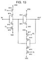
- the shift register illustrated in FIG. 13 includes, as a basic constituent unit, a first clocked inverter consisting of p-channel transistors M13, M14 and n-channel transistors M15, M16, an inverter consisting of a p-channel transistor M12 and an n-channel transistor M11, and a second clocked inverter consisting of p-channel transistors M17, M18 and n-channel transistors M19, M20.
- a clock CL of positive logic is delivered to the p-channel transistor M13 of the first clocked inverter, and a clock -CL of negative logic delivered to the n-channel transistor M16.
- a clock -CL of negative logic is delivered to the p-channel transistor M17 of the second clocked inverter, and a clock CL of positive logic delivered to the n-channel transistor M19.
- the output of the inverter is connected to the input of the second clocked inverter, and the input of the inverter connected to the output of the second clocked inverter.
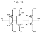
- the shift register illustrated in FIG. 14 includes, as a basic constituent unit, a first inverter consisting of a p-channel transistor M31 and an n-channel transistor M32, a second inverter consisting of a p-channel transistor M33 and an n-channel transistor M34, and a switching circuit interposed between these inverters and consisting of a p-channel transistor M35 and an n-channel transistor M36.
- these shift registers need at least two switching devices until an input signal is transferred to a next stage in synchronization with a clock signal.
- the electric charge charged from a power supply line and discharged therefrom is transferred to a next stage through at least two switching devices.
- the registers encounter difficulty in catching up with high-speed operation.
- the invention provides a shift register comprising switching devices having an active layer formed of polycrystalline silicon, wherein an electric charge that is charged to the shift register through a power supply line and discharged therefrom is transferred to a next stage (M2, M4) through only one switching device (M1, M3).
- the shift register has a pair of switching devices (M1, M3) capable of complimentary operation as an operating unit, wherein a signal is transferred to the next stage (M2, M4) by the pair of switching devices (M1, M3).
- the operating unit is adapted to transfer an input signal to the next stage in synchronization with a clock signal.
- the invention provides a shift register comprising a first pair of switching devices (M1, M3) having an active layer formed of polycrystalline silicon as a first operating unit, the pair of switching devices being capable of complimentary operation and functioning as an inverter, the shift register further comprising a second pair of complimentary, series connected switching devices (M2, M4), wherein a clock signal is fed to a controlled terminal of one (M1) of the first pair of switching devices, an output of the first operating unit is fed to a control terminal of one (M4) of the second pair of switching devices while the clock signal is fed to a control terminal of the other (M4) of the second pair of switching devices, and an output signal is delivered from an intermediate between the second pair of switching devices (M2, M4).
- M1, M3 having an active layer formed of polycrystalline silicon as a first operating unit
- M2 M4 complimentary, series connected switching devices
- the shift register has an off current of up to 1x10 -7 A, and an electric field of up to 0.2 MV/cm is applied between controlled electrodes of each switching device.
- an image display apparatus comprising the shift register defined above.
- the image display apparatus further includes an organic EL device as a pixel.
- the image display apparatus of the invention includes a shift register comprising switching devices having an active layer formed of poly-Si.
- the electric charge that is charged to the shift register through a power supply line and discharged therefrom is transferred to a next stage M2, M4 through only one switching device M1, M3.
- the shift register has a pair of switching devices M1, M3 capable of complimentary operation as an operating unit, and the pair of switching devices M1, M3 transfer a signal to the next stage M2, M4.
- This operating unit transfers an input signal to the next stage in synchronization with a clock signal.
- the shift register has a first pair of switching devices M1, M3 whose active layer is formed of poly-Si as a first operating unit, the pair of switching devices being capable of complimentary operation and functioning as an inverter, and a second pair of complimentary, series connected switching devices M2, M4.
- a clock signal is fed to a controlled terminal of one switching device M1 of the first pair, an output of the first operating unit is fed to a control terminal of one switching device M4 of the second pair while the clock signal is fed to a control terminal of the other switching device M4 of the second pair, and an output signal is delivered from an intermediate between the second pair of switching devices M2, M4.
- a clock signal rather than a power supply is fed to one of the controlled terminals of push-pull connected (or complementary) switching devices.
- one switching device receives at its control terminal the output signal from the first stage, the other switching device receives at its control terminal the clock signal, and an output is delivered from the intermediate between theses switching devices. Then the input signal is transferred in synchronization with the clock by way of only one switching device, whereby the output signal delayed by one clock is delivered.
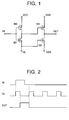
- FIG. 1 is a circuit diagram showing one exemplary arrangement of the shift register according to the invention.
- FIG. 2 is a timing chart showing the operation of the circuit.
- a first stage consists of a pair of first and third switching devices M1 and M3 having control terminals or gates both connected to an input terminal IN.
- the first switching device M1 has a pair of controlled terminals one (source) of which is connected to a clock input terminal CL.
- the other controlled terminal (drain) of the first switching device M1 is connected to one controlled terminal (drain) of the third switching device M3.
- Connected to the other controlled terminal (source) of the third switching device M3 is a power supply VDD.
- the first and third switching devices M1 and M3 of the first stage a pair of switching devices capable of complimentary operation or push-pull operation are preferably selected and used.
- the first switching device M1 is of N type and the third switching device M3 is of P type.
- a next stage consists of a pair of second and fourth switching devices M2 and M4.
- the second switching device M2 has a control terminal or gate connected to the clock input terminal CL.
- One controlled terminal (drain) of the second switching device M2 is connected to one controlled terminal (drain) of the fourth switching device M4 and to an output terminal OUT.
- the other controlled terminal (source) of the second switching device M2 is connected to a negative power supply VSS.
- the control terminal of the fourth switching device M4 is connected to both the controlled terminal (drain) of the first switching device M1 and the controlled terminal (drain) of the third switching device M3 of the first stage. Connected to the other controlled terminal (source) of the fourth switching device M4 is a power supply VDD.
- the second and fourth switching devices M2 and M4 of the next stage a pair of switching devices capable of complimentary operation or push-pull operation are preferably selected and used.
- the second switching device M2 is of N type and the fourth switching device M4 is of P type.
- the shift register of the illustrated construction upon receipt of an input pulse signal as shown in FIG. 2, it is provided to the control terminals of the first and third switching devices M1 and M3 in the first stage.
- the first and third switching devices M1 and M3 operate in accordance with the input signal while a clock signal is fed to the controlled terminal of the first switching device M1.
- the input signal is admitted in synchronization with the clock signal and transferred to the next stage as an output signal.
- the fourth switching device M4 of the next stage operates in accordance with the output signal from the first stage while the second switching device M2 in cascade connection therewith operates in accordance with the clock signal CL. Consequently, the output of these switching devices is also delivered in accordance with the clock signal. Since the first stage operates such that the signal is processed at the fall of the clock signal and the next stage operates such that the signal is processed at the rise of the clock signal, the output signal is delayed by one clock as shown in FIG. 2.
- the switching devices used herein may be conventional bipolar transistors or field effect transistors (FET) and especially, thin film transistors (TFT) of c-MOS type.
- FET field effect transistors
- TFT thin film transistors
- the shift register of the invention favors an off current of up to 1x10 -7 A, and especially up to 1x10 -8 A.
- the lower limit of the off current is not critical although it is usually about 1x10 -10 A. An off current above the limit may adversely affect stability.
- the electric field applied between the controlled terminals (drain and source) of the switching device is preferably up to 0.2 MV/cm, and especially up to 0.1 MV/cm.
- the lower limit of the electric field is not critical although it is usually about 0.05 MV/cm. An electric field intensity above the limit may adversely affect stability.
- the shift register of the invention provides for a maximum operating frequency of about twice greater than conventional shift registers using poly-Si.
- the shift register of the invention is not critical as long as the active layers of the switching devices are constructed of poly-Si and high-speed operation is required in its application. It is useful in a variety of applications, and especially liquid crystal and inorganic and organic EL image display apparatus.
- the shift register of the invention is combined with an organic EL device, which is a self light-emitting device capable of fast operation, to construct an image display apparatus.
- the organic EL device includes first and second electrodes, and an organic layer disposed therebetween and containing at least an organic material participating in a light emitting function.
- the first and second electrodes supply electrons and holes to the organic layer where they are recombined to emit light.
- Either of the first and second electrodes may be a hole or electron injecting electrode.
- the first electrode disposed closer to the substrate is a hole injecting electrode and the second electrode remote from the substrate is an electron injecting electrode.
- the electron injecting electrode is preferably made of a material having a low work function, for example, a metal element such as K, Li, Na, Mg, La, Ce, Ca, Sr, Ba, Al, Ag, In, Sn, Zn or Zr, and binary or ternary alloys made of two or three such metal elements for stability improvement.
- a metal element such as K, Li, Na, Mg, La, Ce, Ca, Sr, Ba, Al, Ag, In, Sn, Zn or Zr, and binary or ternary alloys made of two or three such metal elements for stability improvement.
- Exemplary alloys are Ag-Mg (Ag: 0.1 to 50 at%), Al-Li (Li: 0.01 to 14 at%), In-Mg (Mg: 50 to 80 at%), and Al-Ca (Ca: 0.01 to 20 at%). It is understood that the electron injecting electrode can be formed by evaporation or sputtering.
- the electron injecting electrode thin film may have a sufficient thickness for electron injection, for example, a thickness of at least 0.5 nm, preferably at least 1 nm, and more preferably at least 3 nm. Although the upper limit is not critical, the electrode thickness is typically about 3 to about 500 nm. On the electron injecting electrode, an auxiliary or protective electrode may be provided, if desired.
- an appropriate pressure is 1x10 -8 to 1x10 -5 Torr and the heating temperature of the evaporation source is about 100°C to about 1,400°C for metal materials and about 100°C to about 500°C for organic materials.
- a transparent or translucent electrode is preferred as the hole injecting electrode so that emitted light may exit from the substrate side.
- Useful materials for transparent electrodes include tin-doped indium oxide (ITO), zinc-doped indium oxide (IZO), zinc oxide (ZnO), tin oxide (SnO 2 ), and indium oxide (In 2 O 3 ), with ITO and IZO being preferred.
- the ITO usually contains In 2 O 3 and SnO 2 in stoichiometry although the oxygen content may deviate somewhat therefrom.
- Opaque, well-known metal materials may be used when the hole injecting electrode need not be transparent.
- the hole injecting electrode should have a sufficient thickness for hole injection and is preferably about 50 to about 500 nm thick, especially about 50 to 300 nm thick. Although no upper limit need be imposed on the thickness of the hole injecting electrode, too thick electrodes can peel off. A too thin electrode is undesirable in film strength, hole transporting capability, and resistivity.
- the hole injecting electrode can be formed by evaporation or other techniques although sputtering, especially pulse DC sputtering is preferable.
- the organic layers in the organic EL structure may be constructed as described below.
- the light emitting layer has functions of injecting holes and electrons, transporting them, and recombining holes and electrons to create excitons. It is preferred to use relatively electronically neutral compounds in the light emitting layer.
- the hole injecting and transporting layer has functions of facilitating injection of holes from the hole injecting electrode, transporting them stably, and blocking electrons.
- the electron injecting and transporting layer has functions of facilitating injection of electrons from the electron injecting electrode, transporting them stably, and blocking holes. These layers are effective for increasing the number of holes and electrons injected into the light emitting layer and confining holes and electrons therein for optimizing the recombination region to improve light emission efficiency.
- the thicknesses of the light emitting layer, hole injecting and transporting layer, and electron injecting and transporting layer are not critical and vary with a particular formation technique. Usually a single layer is about 5 to 500 nm thick, especially about 10 to 300 nm thick.
- the thicknesses of the hole injecting and transporting layer and electron injecting and transporting layer are equal to or range from 1/10 to 10 times the thickness of the light emitting layer although they depend on the design of a recombination/light emitting region.
- the electron or hole injecting and transporting layer is divided into an injecting layer and a transporting layer, preferably the injecting layer is at least 1 nm thick and the transporting layer is at least 1 nm thick.
- the upper limit of thickness is generally about 500 nm for the injecting layer and about 500 nm for the transporting layer. The same applies when two injecting and transporting layers are provided.
- the light emitting layer contains a fluorescent material that is a compound having a light emitting capability.
- the fluorescent material may be at least one member selected from compounds as disclosed, for example, in JP-A 63-264692, such as quinacridone, rubrene, and styryl dyes.
- quinoline derivatives such as metal complex dyes having 8-quinolinol or a derivative thereof as the ligand such as tris(8-quinolinolato)aluminum are included as well as tetraphenylbutadiene, anthracene, perylene, coronene, and 12-phthaloperinone derivatives. Further useful are the phenylanthracene derivatives described in JP-A 8-12600 and the tetraarylethene derivatives described in JP-A 8-12969.
- the fluorescent material in combination with a host material capable of light emission by itself, that is, to use the fluorescent material as a dopant.
- the content of the fluorescent material in the light emitting layer is preferably 0.01 to 20% by volume, especially 0.1 to 15% by volume.
- an appropriate content of rubrene is 0.01 to 20% by volume.
- quinolinolato complexes are preferable, with aluminum complexes having 8-quinolinol or a derivative thereof as the ligand being more preferable.
- aluminum complexes are disclosed in JP-A 63-264692, 3-255190, 5-70773, 5-258859 and 6-215874.
- Illustrative examples include tris(8-quinolinolato)aluminum, bis(8-quinolinolato)magnesium, bis(benzo ⁇ f ⁇ -8-quinolinolato)zinc, bis(2-methyl-8-quinolinolato)aluminum oxide, tris(8-quinolinolato)indium, tris(5-methyl-8-quinolinolato)aluminum, 8-quinolinolatolithium, tris(5-chloro-8-quinolinolato)gallium, bis(5-chloro-8-quinolinolato)calcium, 5,7-dichloro-8-quinolinolatoaluminum, tris(5,7-dibromo-8-hydroxyquinolinolato)aluminum, and poly[zinc(II)-bis(8-hydroxy-5-quinolinyl)methane].
- the light emitting layer may also serve as an electron injecting and transporting layer.
- the use of tris(8-quinolinolato)aluminum and analogues is preferred. These fluorescent materials may be evaporated.
- the light emitting layer is a layer of a mixture of at least one hole injecting and transporting compound and at least one electron injecting and transporting compound, which may contain a dopant.
- the content of the dopant is preferably 0.01 to 20% by volume, especially 0.1 to 15% by volume.
- the mix layer carrier hopping conduction paths are created, allowing carriers to move through a polarly predominant material while injection of carriers of opposite polarity is rather inhibited.
- the organic compound is less susceptible to damage, resulting in the advantage of an extended device life.
- the hole injecting and transporting compound and electron injecting and transporting compound used in the mix layer may be selected from compounds for the hole injecting and transporting layer and compounds for the electron injecting and transporting layer to be described later, respectively.
- the compounds for the hole injecting and transporting layer are preferably amine derivatives having strong fluorescence, for example, triphenyldiamine (TPD) derivatives, styrylamine derivatives and amine derivatives having an aromatic fused ring known as the hole transporting material.
- TPD triphenyldiamine
- the compounds for the electron injecting and transporting layer are preferably quinoline derivatives and metal complexes having 8-quinolinol or a derivative thereof as a ligand, especially tris(8-quinolinolato)aluminum (Alq3).
- the phenylanthracene derivatives and tetraarylethene derivatives described above are also preferably used.
- the weight ratio of the hole injecting and transporting compound to the electron injecting and transporting compound range from about 1/99 to 99/1, more preferably from about 10/90 to 90/10, especially from about 20/80 to 80/20.
- the thickness of the mix layer preferably ranges from the thickness corresponding to a single molecule layer to less than the thickness of an organic compound layer, for example, preferably from 1 to 85 nm, more preferably 5 to 60 nm, most preferably 5 to 50 nm.
- the mix layer is formed by a co-deposition process of evaporating the compounds from distinct sources. If both the compounds have equal or very close vapor pressure or evaporation temperature, they may be pre-mixed in a common evaporation boat, from which they are evaporated together.
- the mix layer is preferably a uniform mixture of both the compounds although the compounds can be present in island form.
- the light emitting layer is generally formed to a predetermined thickness by evaporating an organic fluorescent material or coating a dispersion thereof in a resin binder.
- the hole injecting and transporting layer there may be used various organic compounds as described, for example, in JP-A 63-295695, 2-191694, 3-792, 5-234681, 5-239455, 5-299174, 7-126225, 7-126226, and 8-100172, and EP 0650955A1.
- exemplary are tetraarylbenzidine compounds (triaryldiamines or triphenyldiamines: TPD), aromatic tertiary amines, hydrazone derivatives, carbazole derivatives, triazole derivatives, imidazole derivatives, oxadjazole derivatives having an amino group, and polythiophenes. Two or more of these compounds may be used, and on such combined use, they may be formed as separate layers or mixed.
- the hole injecting and transporting layer is formed separately as a hole injecting layer and a hole transporting layer
- two or more compounds are selected in a proper combination from the compounds commonly used in hole injecting and transporting layers.
- laminate layers in such an order that a layer of a compound having a lower ionization potential may be disposed adjacent the hole injecting electrode (ITO).
- ITO hole injecting electrode
- the order of lamination also applies where a plurality of hole injecting and transporting layers are provided. Such an order of lamination is effective for lowering the drive voltage and preventing current leakage and the development and growth of dark spots.
- the hole injecting and transporting layer may be formed by evaporating the above-mentioned compounds.
- the electron injecting and transporting layer there may be used quinoline derivatives including organic metal complexes having 8-quinolinol or a derivative thereof as a ligand such as tris(8-quinolinolato)aluminum (Alq3). oxadiazole derivatives, perylene derivatives, pyridine derivatives, pyrimidine derivatives, quinoxaline derivatives, diphenyiquinone derivatives, and nitro-substituted fluorene derivatives.
- the electron injecting and transporting layer can also serve as the light emitting layer. In this case, use of tris(8-quinolinolato)aluminum etc. is preferred.
- the electron injecting and transporting layer may be formed by evaporation or the like.
- the electron injecting and transporting layer is formed separately as an electron injecting layer and an electron transporting layer
- two or more compounds are selected in a proper combination from the compounds commonly used in electron injecting and transporting layers.
- the order of stacking also applies where a plurality of electron injecting and transporting layers are provided.
- vacuum evaporation is preferably used because homogeneous thin films are available.
- vacuum evaporation there is obtained a homogeneous thin film which is amorphous or has a crystal grain size of less than 0.2 ⁇ m. If the grain size is more than 0.2 ⁇ m, uneven light emission would take place and the drive voltage of the device must be increased with a substantial drop of charge injection efficiency.
- the conditions for vacuum evaporation are not critical although a vacuum of 10 -4 Pa or lower and a deposition rate of about 0.01 to 1 nm/sec are preferred. It is preferred to successively form layers in vacuum because the successive formation in vacuum can avoid adsorption of impurities on the interface between the layers, thus ensuring better performance. Also, the drive voltage of a device can be reduced and the development and growth of dark spots be restrained.
- boats having the compounds received therein are individually temperature controlled to achieve co-deposition.
- the substrate may be provided with a color filter film, a fluorescent material-containing color conversion film or a dielectric reflecting film for controlling the color of light emission.
- the color filter film used herein may be a color filter as used in liquid crystal displays and the like.
- the properties of a color filter may be adjusted in accordance with the light emission of the organic EL device so as to optimize the extraction efficiency and color purity.
- a color filter capable of cutting external light of short wavelength which is otherwise absorbed by the EL device materials and fluorescent conversion layer, because the light resistance and display contrast of the device are improved.
- An optical thin film such as a dielectric multilayer film may be used instead of the color filter.
- the organic EL device used herein is generally of the dc or pulse drive type.
- the applied voltage is generally about 2 to 30 volts.
- TFT thin film transistor
- a polycrystalline silicon layer having a grain size of the order of 0.5 to 2 ⁇ m can be formed.
- the TFT using this as the active layer has an N channel mobility of about 100 cm 2 /V ⁇ S and a threshold of about 0.5 V. It is noted that the above-described materials and parameters are given merely for illustrative purposes.
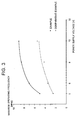
- a shift register represented by the circuit diagram of FIG. 1 was formed in accordance with the above-mentioned process.
- a shift register having 648 stages of constituent units shown by the circuit diagram of FIG. 1 was formed. While clock pulses were supplied, input signals are fed to the shift register to see if the shift register operated normally. It was confirmed that a delay signal was delivered from the output of each stage in synchronization with the clock pulse.
- the operating frequency of the shift register of the invention is about twice greater than that of the comparative shift register at every power supply voltage.
- an image display apparatus was constructed using the shift register of Example 1 and organic EL devices capable of high speed operation as image display devices.
- TFTs for driving the organic EL devices serving as pixels were formed as follows. First, an amorphous silicon layer of about 600 ⁇ was deposited on a substrate by a CVD technique. The depositing conditions included 100 SCCM of Si 2 H 6 gas, a pressure of 0.3 Torr, and a temperature of 480°C.
- the amorphous silicon layer was then converted into an active layer (polycrystalline silicon layer) by solid phase growth.
- the solid phase growth was effected by heat annealing followed by laser annealing.
- the heat annealing conditions included 1 SLM of N 2 , a temperature of 600°C, and a treating time of 24 hours.
- the laser annealing used a KrF excimer laser of 254 nm, with an energy density of 200 mJ/cm 2 and 50 shots.
- the poly-Si layer was then patterned, leaving an active silicon layer of 500 ⁇ .
- a SiO 2 layer serving as a gate oxide film was deposited to a thickness of about 800 ⁇ by a plasma CVD technique.
- the deposition conditions included an input power of 50 W, 50 SCCM of TEOS, 500 SCCM of O 2 , a pressure of 0.1 to 0.5 Torr, and a temperature of 350°C.
- a Mo-Si 2 layer serving as a gate electrode was deposited to a thickness of about 1,000 ⁇ by sputtering.
- the Mo-Si 2 layer and the previously formed SiO 2 layer were then patterned as by dry etching, obtaining a gate electrode and a gate oxide film.
- the structure was then heated in a nitrogen atmosphere at about 550°C for 10 hours for activating the dopants.
- the structure was further heated in a hydrogen atmosphere at about 400°C for 30 minutes for effecting hydrogenation to reduce the defect level density of the semiconductor layer.
- a SiO 2 layer serving as an interlayer insulating layer was formed to a thickness of about 8,000 ⁇ .
- the conditions under which SiO 2 was deposited included 10 SLM of O 2 /N 2 , 1 SLM of N 2 containing 5% of SiH 4 , 500 SCCM of N 2 containing 1% of PH 3 , 10 SLM of N 2 , a temperature of 410°C, and atmospheric pressure.
- the SiO 2 film serving as an interlayer insulating layer was etched to form contact holes. Aluminum was then evaporated to form drain and source wiring electrodes.
- the resulting TFT array had an off current of 4x10 -10 A and an electric field of up to 0.2 MV/cm between drain and source.
- ITO indium tin oxide
- organic layers including a hole injecting and transporting layer, a light emitting layer and a high-resistance electron injecting and transporting layer were formed by vacuum evaporation.
- the materials evaporated herein are shown below. Only exemplary materials are described herein although any desired material which can be deposited by evaporation is applicable as understood from the above-described concept of organic EL device.
- the substrate on which the ITO electrode layer etc. had been formed was cleaned on its surface with UV/O 3 , it was secured by a holder in a sputtering chamber, which was evacuated below 1x10 -4 Pa.
- N,N,N',N'-tetrakis(m-biphenyl)-1,1'-biphenyl-4,4'-diamine was evaporated at a deposition rate of 0.2 nm/sec to a thickness of 200 nm, forming a hole injecting and transporting layer.
- TPD tris(8-quinolinolato)aluminum
- Alq3 tris(8-quinolinolato)aluminum
- rubrene was evaporated at an overall deposition rate of 0.2 nm/sec to a thickness of 100 nm, forming a light emitting layer.
- the layer contained TPD and Alq3 in a volume ratio of 1:1 which was doped with 10% by volume of rubrene.
- the substrate was then transferred to a sputtering chamber.
- a target of Li 2 O having 4 mol% of V mixed therewith a high-resistance inorganic electron injecting and transporting layer was deposited to a thickness of 10 nm.
- the sputtering conditions included 30 SCCM of Ar, 5 SCCM of O 2 , room temperature (25°C), a deposition rate of 1 nm/min, an operating pressure of 0.2 to 2 Pa, and an input power of 500 W.
- the inorganic electron injecting layer thus deposited had substantially the same composition as the target.
- the organic EL display apparatus When the organic EL display apparatus thus obtained was driven in air at a constant current density of 10 mA/cm 2 , it operated normally with an initial luminance of 800 cd/m 2 and a drive voltage of 7.5 V. It was also confirmed that the pixel that was selected in accordance with the operation of the shift register was driven.
Applications Claiming Priority (2)
| Application Number | Priority Date | Filing Date | Title |
|---|---|---|---|
| JP27630099 | 1999-09-29 | ||
| JP27630099A JP2001100653A (ja) | 1999-09-29 | 1999-09-29 | シフトレジスタおよび画像表示装置 |
Publications (2)
| Publication Number | Publication Date |
|---|---|
| EP1089291A2 true EP1089291A2 (de) | 2001-04-04 |
| EP1089291A3 EP1089291A3 (de) | 2001-09-19 |
Family
ID=17567538
Family Applications (1)
| Application Number | Title | Priority Date | Filing Date |
|---|---|---|---|
| EP00308170A Withdrawn EP1089291A3 (de) | 1999-09-29 | 2000-09-19 | Schieberegister und Anzeigegerät mit diesem Schieberegister |
Country Status (3)
| Country | Link |
|---|---|
| EP (1) | EP1089291A3 (de) |
| JP (1) | JP2001100653A (de) |
| KR (1) | KR20010050331A (de) |
Cited By (1)
| Publication number | Priority date | Publication date | Assignee | Title |
|---|---|---|---|---|
| CN110728945A (zh) * | 2019-11-27 | 2020-01-24 | 京东方科技集团股份有限公司 | 移位寄存器单元及其驱动方法、栅极驱动电路和显示装置 |
Families Citing this family (2)
| Publication number | Priority date | Publication date | Assignee | Title |
|---|---|---|---|---|
| CN104599630B (zh) * | 2014-12-16 | 2017-04-19 | 上海天马有机发光显示技术有限公司 | 一种驱动电路及发光控制电路、显示面板、显示装置 |
| JP2019091516A (ja) * | 2017-11-15 | 2019-06-13 | シャープ株式会社 | シフトレジスタおよびそれを備えた表示装置 |
Citations (2)
| Publication number | Priority date | Publication date | Assignee | Title |
|---|---|---|---|---|
| EP0837445A1 (de) * | 1996-10-18 | 1998-04-22 | Canon Kabushiki Kaisha | Aktiv-Matrix-Substrat mit Zeilen- und Spaltentreibern für Flüssigkristallanzeige |
| JPH1185114A (ja) * | 1997-09-12 | 1999-03-30 | Sanyo Electric Co Ltd | データ線駆動回路 |
-
1999
- 1999-09-29 JP JP27630099A patent/JP2001100653A/ja not_active Withdrawn
-
2000
- 2000-09-04 KR KR1020000052105A patent/KR20010050331A/ko not_active Application Discontinuation
- 2000-09-19 EP EP00308170A patent/EP1089291A3/de not_active Withdrawn
Patent Citations (2)
| Publication number | Priority date | Publication date | Assignee | Title |
|---|---|---|---|---|
| EP0837445A1 (de) * | 1996-10-18 | 1998-04-22 | Canon Kabushiki Kaisha | Aktiv-Matrix-Substrat mit Zeilen- und Spaltentreibern für Flüssigkristallanzeige |
| JPH1185114A (ja) * | 1997-09-12 | 1999-03-30 | Sanyo Electric Co Ltd | データ線駆動回路 |
Non-Patent Citations (1)
| Title |
|---|
| HIROYUKI SEKINE ET AL: "HIGH-SPEED LINEAR IMAGE SENSOR WITH A SINGLE-PHASE-CLOCK POLY-SI TFT DRIVER" NEC RESEARCH AND DEVELOPMENT,JP,NIPPON ELECTRIC LTD. TOKYO, vol. 37, no. 2, 1 April 1996 (1996-04-01), pages 226-233, XP000621991 ISSN: 0547-051X * |
Cited By (1)
| Publication number | Priority date | Publication date | Assignee | Title |
|---|---|---|---|---|
| CN110728945A (zh) * | 2019-11-27 | 2020-01-24 | 京东方科技集团股份有限公司 | 移位寄存器单元及其驱动方法、栅极驱动电路和显示装置 |
Also Published As
| Publication number | Publication date |
|---|---|
| JP2001100653A (ja) | 2001-04-13 |
| EP1089291A3 (de) | 2001-09-19 |
| KR20010050331A (ko) | 2001-06-15 |
Similar Documents
| Publication | Publication Date | Title |
|---|---|---|
| US6369507B1 (en) | Organic EL display apparatus with a switching device | |
| JP2001195014A (ja) | 有機el素子の駆動装置 | |
| US6876007B2 (en) | Light emitting device driving by alternating current in which light emission is always obtained | |
| US7619244B2 (en) | Organic light emitting display apparatus | |
| US6882105B2 (en) | Organic light-emitting display device | |
| JP2001134217A (ja) | 有機el素子の駆動装置 | |
| US20090146930A1 (en) | Organic electro-luminescent display apparatus | |
| JP2006324537A (ja) | 表示装置 | |
| JP2005276542A (ja) | 有機発光表示装置 | |
| US6590554B1 (en) | Color image display system | |
| JP2001183996A (ja) | 画像表示装置および薄膜表示素子の駆動方法 | |
| US20010010374A1 (en) | Thin-film display system | |
| EP1089291A2 (de) | Schieberegister und Anzeigegerät mit diesem Schieberegister | |
| JP2001060691A (ja) | 半導体装置 | |
| JP4091021B2 (ja) | アクティブマトリックス型の表示装置 | |
| JP4246845B2 (ja) | 有機el素子の駆動装置および有機el表示装置 | |
| JP2000340359A (ja) | 有機el素子の駆動装置および有機el表示装置 | |
| JP2000340358A (ja) | 有機el素子の駆動装置および有機el表示装置 | |
| WO2004032577A1 (ja) | 有機el積層型有機スイッチング素子及び有機elディスプレイ | |
| JP4792634B2 (ja) | 光機能素子、有機el素子および有機el表示装置 | |
| KR100669415B1 (ko) | 박막 트랜지스터 제조 방법 | |
| JP2002270367A (ja) | 光機能素子、有機el素子および有機el表示装置 | |
| JP2000307119A (ja) | 有機el素子の駆動装置および有機el表示装置 |
Legal Events
| Date | Code | Title | Description |
|---|---|---|---|
| PUAI | Public reference made under article 153(3) epc to a published international application that has entered the european phase |
Free format text: ORIGINAL CODE: 0009012 |
|
| AK | Designated contracting states |
Kind code of ref document: A2 Designated state(s): AT BE CH CY DE DK ES FI FR GB GR IE IT LI LU MC NL PT SE |
|
| AX | Request for extension of the european patent |
Free format text: AL;LT;LV;MK;RO;SI |
|
| PUAL | Search report despatched |
Free format text: ORIGINAL CODE: 0009013 |
|
| AK | Designated contracting states |
Kind code of ref document: A3 Designated state(s): AT BE CH CY DE DK ES FI FR GB GR IE IT LI LU MC NL PT SE |
|
| AX | Request for extension of the european patent |
Free format text: AL;LT;LV;MK;RO;SI |
|
| RIC1 | Information provided on ipc code assigned before grant |
Free format text: 7G 11C 19/28 A, 7G 09G 3/36 B |
|
| AKX | Designation fees paid | ||
| REG | Reference to a national code |
Ref country code: DE Ref legal event code: 8566 |
|
| STAA | Information on the status of an ep patent application or granted ep patent |
Free format text: STATUS: THE APPLICATION IS DEEMED TO BE WITHDRAWN |
|
| 18D | Application deemed to be withdrawn |
Effective date: 20020320 |