EP1083602A2 - Lead frame and resin package and photoelectron device using the same - Google Patents
Lead frame and resin package and photoelectron device using the same Download PDFInfo
- Publication number
- EP1083602A2 EP1083602A2 EP00119722A EP00119722A EP1083602A2 EP 1083602 A2 EP1083602 A2 EP 1083602A2 EP 00119722 A EP00119722 A EP 00119722A EP 00119722 A EP00119722 A EP 00119722A EP 1083602 A2 EP1083602 A2 EP 1083602A2
- Authority
- EP
- European Patent Office
- Prior art keywords
- die pad
- inner leads
- lead
- leads
- thickness
- Prior art date
- Legal status (The legal status is an assumption and is not a legal conclusion. Google has not performed a legal analysis and makes no representation as to the accuracy of the status listed.)
- Withdrawn
Links
Images



Classifications
-
- H—ELECTRICITY
- H10—SEMICONDUCTOR DEVICES; ELECTRIC SOLID-STATE DEVICES NOT OTHERWISE PROVIDED FOR
- H10W—GENERIC PACKAGES, INTERCONNECTIONS, CONNECTORS OR OTHER CONSTRUCTIONAL DETAILS OF DEVICES COVERED BY CLASS H10
- H10W72/00—Interconnections or connectors in packages
-
- H—ELECTRICITY
- H10—SEMICONDUCTOR DEVICES; ELECTRIC SOLID-STATE DEVICES NOT OTHERWISE PROVIDED FOR
- H10W—GENERIC PACKAGES, INTERCONNECTIONS, CONNECTORS OR OTHER CONSTRUCTIONAL DETAILS OF DEVICES COVERED BY CLASS H10
- H10W70/00—Package substrates; Interposers; Redistribution layers [RDL]
- H10W70/40—Leadframes
- H10W70/461—Leadframes specially adapted for cooling
-
- H—ELECTRICITY
- H10—SEMICONDUCTOR DEVICES; ELECTRIC SOLID-STATE DEVICES NOT OTHERWISE PROVIDED FOR
- H10F—INORGANIC SEMICONDUCTOR DEVICES SENSITIVE TO INFRARED RADIATION, LIGHT, ELECTROMAGNETIC RADIATION OF SHORTER WAVELENGTH OR CORPUSCULAR RADIATION
- H10F77/00—Constructional details of devices covered by this subclass
- H10F77/50—Encapsulations or containers
-
- H—ELECTRICITY
- H10—SEMICONDUCTOR DEVICES; ELECTRIC SOLID-STATE DEVICES NOT OTHERWISE PROVIDED FOR
- H10W—GENERIC PACKAGES, INTERCONNECTIONS, CONNECTORS OR OTHER CONSTRUCTIONAL DETAILS OF DEVICES COVERED BY CLASS H10
- H10W70/00—Package substrates; Interposers; Redistribution layers [RDL]
- H10W70/40—Leadframes
- H10W70/411—Chip-supporting parts, e.g. die pads
-
- H—ELECTRICITY
- H10—SEMICONDUCTOR DEVICES; ELECTRIC SOLID-STATE DEVICES NOT OTHERWISE PROVIDED FOR
- H10W—GENERIC PACKAGES, INTERCONNECTIONS, CONNECTORS OR OTHER CONSTRUCTIONAL DETAILS OF DEVICES COVERED BY CLASS H10
- H10W70/00—Package substrates; Interposers; Redistribution layers [RDL]
- H10W70/40—Leadframes
- H10W70/421—Shapes or dispositions
-
- H—ELECTRICITY
- H10—SEMICONDUCTOR DEVICES; ELECTRIC SOLID-STATE DEVICES NOT OTHERWISE PROVIDED FOR
- H10W—GENERIC PACKAGES, INTERCONNECTIONS, CONNECTORS OR OTHER CONSTRUCTIONAL DETAILS OF DEVICES COVERED BY CLASS H10
- H10W70/00—Package substrates; Interposers; Redistribution layers [RDL]
- H10W70/40—Leadframes
- H10W70/421—Shapes or dispositions
- H10W70/424—Cross-sectional shapes
-
- H—ELECTRICITY
- H10—SEMICONDUCTOR DEVICES; ELECTRIC SOLID-STATE DEVICES NOT OTHERWISE PROVIDED FOR
- H10H—INORGANIC LIGHT-EMITTING SEMICONDUCTOR DEVICES HAVING POTENTIAL BARRIERS
- H10H20/00—Individual inorganic light-emitting semiconductor devices having potential barriers, e.g. light-emitting diodes [LED]
- H10H20/80—Constructional details
- H10H20/85—Packages
- H10H20/857—Interconnections, e.g. lead-frames, bond wires or solder balls
Definitions
- the present invention relates to a lead frame and a resin package using the lead frame. Furthermore, the present invention relates to a miniature photoelectron device on which a high output semiconductor laser is mounted, using the resin package.
- a photoelectron device including an optical semiconductor element is known, for example, from JP 6-203403A.
- This publication discloses the following photoelectron device.
- a lead frame including a die pad and inner leads whose end portions are arranged in the vicinity of the periphery of the die pad is produced, and then the lead frame is sealed with a resin to produce a resin package.
- This resin package is provided with an opening for exposing the the pad and the end portions of the inner leads.
- an optical semiconductor element is mounted on the the pad in the opening, and the electrodes of the optical semiconductor element are connected by wiring to the corresponding end portions of the inner leads exposed in the periphery of the die pad.
- a transparent optical member is provided in the opening to seal the optical semiconductor element.
- such a photoelectron device is mounted on an optical pick-up device or the like that records and/or reproduces an optical recording medium such as an optical disk.
- One approach to promote the miniaturization of the photoelectron device is to attain a finer pitch for inner leads constituting a lead frame.
- JP 5-326788A discloses a semiconductor device including fine pitched inner leads, produced by pressing the end portions of the inner leads of multiple pins to reduce the thickness.
- the end portions of the inner leads of the lead frame produced by rolling are pressed so that the thickness thereof is reduced to 1/6 at the largest, and thus thinner inner leads can be obtained.
- the photoelectron device for optical pick-up miniaturization is desired, particularly in one direction of the package for convenience in its installation and arrangement.
- the conventional photoelectron devices are substantially rectangular in plan, and it is becoming difficult to attain further reduction of the size in the direction of the shorter side of the rectangle.
- a first lead frame of the present invention includes a the pad including a the pad main portion having a large thickness and a die pad peripheral portion having an intermediate thickness smaller than that of the die pad main portion, provided on at least one side of the die pad main portion, at least one support lead connected to the die pad, and at least two first inner leads having a small thickness smaller than that of the die pad peripheral portion, arranged such that the end portions thereof are opposed to the the pad peripheral portion.
- the pad peripheral portion having an intermediate thickness is formed on the side of the die pad main portion to which the first inner leads are opposed.
- the region having an intermediate thickness is provided between the thick region and the thin region having significantly different thicknesses, a drastic change in the thickness can be eliminated, and the regions can be formed at one time by rolling.
- the thickness of the the pad necessary for heat release properties and the reduction of the thickness of the end portions of the inner leads necessary for fine pitch can be achieved at the same time.
- miniature leads can be formed easily by press stamping. Therefore, the lead frame including the fine pitched inner leads and the die pad having good heat release properties can be obtained easily and inexpensively.
- a second lead frame of the present invention includes a die pad including a die pad main portion having a large thickness, at least one support lead connected to the die pad, and at least three first inner leads having a small thickness smaller than that of the die pad main portion, arranged such that the end portions thereof are opposed to at least one side of the die pad.
- Each first inner lead has a narrow portion having a small width and a wide portion having a width larger than that of the narrow portion. The narrow portion is positioned on the die pad side, and the wide portion is positioned on the side opposite to the die pad.
- a connection point between the narrow portion and the wide portion of the central first inner lead of the at least three first inner leads is positioned farther from the die pad than connection points between the narrow portions and the wide portions of first inner leads adjacent to the central first inner lead.
- the gap between the central first inner lead and the adjacent first inner leads is smaller in the narrow portion than in the wide portion.
- the inner lead positioned farther from the center has a connection point nearer the die pad.
- the first inner lead positioned farther from the center has the longer wide portion. Therefore, the strength of the thin first inner leads can be kept high even in the vicinity of the end portions thereof. Therefore, deformation can be suppressed during processing. The strength of the exposed end portions from the sealing resin can be improved, and deformation hardly occurs. Thus, peeling from the resin after resin-sealing can be suppressed.
- the lead gap is smaller in the narrow portion, fine pitched first inner leads can be achieved as well. Furthermore, the thick die pad main portion allows good heat release properties.
- a third lead frame of the present invention includes a belt-shaped thick region having a large thickness and a belt-shaped thin region having a thickness smaller than that of the thick region, these regions being in parallel with each other.
- a die pad is formed in the thick region, and leads are formed in the thin region, and the leads extend in a direction substantially perpendicular to that of the belt-shaped region.
- a die pad is formed in a belt-shaped thick region, so that the heat release properties are good.
- Leads are formed in a belt-shaped thin region, so that fine pitched leads can be attained. These belt-shaped regions having different thicknesses are in parallel with each other, and therefore can be obtained easily by rolling.
- the leads extend in the direction substantially perpendicular to the direction in which the belt-shaped regions are formed, the thickness of the leads in the extending direction is uniform. Therefore, fine pitched leads can be produced easily and highly precisely.
- the processed leads hardly are deformed.
- a lead frame having fine pitched inner leads and good heat release properties can be obtained easily and inexpensively.
- a first resin package of the present invention includes a die pad including a die pad main portion having a large thickness and a die pad peripheral portion having an intermediate thickness smaller than that of the die pad main portion, provided on at least one side of the die pad main portion, at least one support lead connected to the die pad, at least two first inner leads having a small thickness smaller than that of the die pad peripheral portion, arranged such that the end portions thereof are opposed to the die pad peripheral portion, and a resin for sealing the die pad, the support lead and the first inner leads for integration while exposing a part of an upper surface and a part of a lower surface of the die pad and upper surfaces of the end portions of the first inner leads.
- the first resin package is obtained by sealing the first lead frame with a resin, and this embodiment allows a resin package with good heat release properties including fine pitched inner leads to be manufactured easily and inexpensively.
- a second resin package of the present invention includes a die pad including a die pad main portion having a large thickness, at least one support lead connected to the die pad, at least three first inner lead having a small thickness smaller than that of the die pad main portion, arranged such that the end portions thereof are opposed to at least one side of the die pad, a resin for sealing the die pad, the support lead and the first inner leads for integration while exposing a part of the upper surface and a part of the lower surface of the the pad and upper surfaces of the end portions of the first inner leads.
- Each first inner lead has a narrow portion having a small width and a wide portion having a width larger than that of the narrow portion. The narrow portion is positioned on the the pad side, and the wide portion is positioned on the side opposite to the die pad.
- a connection point between the narrow portion and the wide portion of the central first inner lead of the at least three first inner leads is positioned farther from the die pad than connection points between the narrow portions and the wide portions of first inner leads adjacent to the central first inner lead.
- the gap between the central first inner lead and the adjacent first inner leads is smaller in the narrow portion than in the wide portion.
- the second resin package is obtained by sealing the second lead frame with a resin, and reduces peeling of the fine pitched first inner leads from the resin. Furthermore, the strength of the end portions exposed from the sealing resin can be improved.
- the thick die pad main portion allows good heat release properties.
- a photoelectron device of the present invention includes the first or second resin package, a photoelectron element mounted on the upper surface of the die pad, and an optically transparent member for sealing the photoelectron element.
- Such a photoelectron device has fine pitched inner leads, it can be miniature, and since it has a thick die pad, the heat release properties can be good.
- Such a photoelectron device can be manufactured easily and inexpensively.
- FIG. 1 is a plan view of a lead frame of the present invention.
- FIG. 2 is a cross-sectional view taken along line II-II of FIG. 1 from the direction indicated by the arrow.
- a lead frame 100 is obtained by rolling a plate-like metal member in a direction indicated by arrow 150, forming a plurality of belt-shaped regions that have different thicknesses parallel to the rolling direction 150, and press-stamping the rolled metal member into a pattern in plan as shown in FIG. 1. More specifically, the lead frame has belt-shaped regions parallel to the rolling direction 150, and the belt-shaped regions have a thickness of t0, t1, t2, or t3, where t0 > t1 ⁇ t2 ⁇ t3 is satisfied. The upper surfaces of the regions are present substantially on a common plane, and the thickness of the each region is changed by changing the position of the lower surface.
- FIG. 1 shows only two repeating units, but a practical lead frame has a large number of such units that are repeated continuously in the roiling direction 150.
- the shape in plan of the die pad 200 is substantially rectangular, and the the pad 200 is provided in such a manner that the shorter side of the rectangle is parallel to the rolling direction 150.
- the lead frame further includes a plurality of leads extending in the direction substantially perpendicular to the rolling direction 150 on the sides of both shorter sides of the die pad 200.
- Each lead is thinner than the die pad peripheral portion 201 having an intermediate thickness (t2), and has at least two variations in thickness. More specifically, each lead has a portion with a thickness t0 of 0.25 to 0.3mm on the outer lead side and a thinner portion with a small thickness t1 of around 0.2mm on the inner lead side.
- the leads are provided so as to extend in the direction substantially perpendicular to the rolling direction 150 so that each portion of the lead in the extending direction can be uniform in thickness. Therefore, a fine pitching process of the leads can be performed with ease and with high precision. Furthermore, the processed leads are hardly deformed.
- the die pad 200 is connected to a support lead 110 so as to be held.
- a connection portion 111 of the support lead 110 that is connected to the the pad 200 has a small thickness (t1), and the width W thereof in the rolling direction 150 is larger than that of other leads for the strength purpose.
- the width W preferably is about 1.5 to 3 times larger than the width in the same direction of the end portions of first inner leads 101, which will be described later.
- the first inner leads 101 are provided in such a manner that the end portions thereof are opposed to the shorter side of the die pad 200.
- five first inner leads 101 are arranged on each of the right and left sides of the die pad 200.
- the width (L1) of the end portion of each first inner lead 101 is 0.15mm.
- the arrangement gap (L2) between the end portions of the first inner leads 101 is 0.15mm.
- the first inner leads 101 are connected to outer leads 103 on the side opposite to the die pad 200.
- the width (L3) of each outer lead 103 is 0.25mm.
- the arrangement gap (L4) between the outer leads 103 is 0.25mm.
- the support lead 110 is connected to the same outer lead 103 as above on the side opposite to the die pad 200.
- the distinction between "inner” and “outer” used herein with the leads is based on whether the leads are exposed from the periphery of a resin package produced by resin sealing as described later.
- each first inner lead 101 has two variations, that is, a small width on the end portion side (on the side of the die pad 200) and a larger width on the opposite side (on the side of the outer lead 103).
- a portion having a small width is referred to as “narrow portion” and a portion having a width larger than that of the narrow portion is referred to as "wide portion”.
- the position of the point (connection point) at which the narrow portion is turned into the wide portion is determined by the position of the first inner lead 101. More specifically, the central first inner lead of the five first inner leads arranged on one side of the die pad 200 has a connection point at the position farthest from the die pad 200, when compared with the other first inner leads.
- the two first inner leads adjacent to the central inner lead have connection points at positions nearer the die pad 200 than the central first inner lead.
- the two outermost first inner leads have connection points at positions even nearer the die pad 200. While varying the positions of the connection points in this manner, the gap between the first inner leads 101 is smaller in the narrow portion than in the wide portion. As a result, the first inner lead 101 positioned farther from the central first inner lead has the longer wide portion. Therefore, the strength of the thin first inner leads can be kept high even in the vicinity of the end portion thereof. Consequently, deformation during processing can be suppressed. Furthermore, the strength of the end portions exposed from a sealing resin can be improved, so that deformation hardly occurs. Therefore, peeling from the resin can be suppressed when resin sealing is performed as described later. Moreover, in addition to these effects, fine pitched end portions of first inner leads 101 can be achieved.
- each lead is formed by rolling to a predetermined thickness and then each lead is provided with a predetermined width by press stamping.
- the gap between the leads and between the leads and the die pad 200 is substantially equal to the width of the lead. Since the thickness of the lead can be reduced, miniaturization can be possible with press stamping, and pressing for correcting deformation of the leads is not necessary after processing.
- the heat release properties become better.
- the die pad peripheral portion 201 having a thickness t2 (t0 ⁇ t2 ⁇ t3) is provided in the periphery of the die pad 200. With this portion, the variation extent can be changed stepwise during formation. Thus, rolling formability can be better (buffer effect).
- the thickness of the leads is effective to achieve fine pitched leads.
- the die pad peripheral portion 201 having an intermediate thickness between the thickness of the thin lead and the thickness of the thick die pad is formed to improve the rolling formability (buffer effect).
- fine pitched thin inner leads can be arranged with high precision between a length of about 1mm, which is the length of the shorter side of the die pad 200.
- a thin second inner lead 102 having a thickness t1 and a width L3 is formed outside the arranged plurality of first inner leads 101.
- the end portion of the second inner lead 102 having the same width L3 and thickness t1 curves toward the gap between the end portions of the first inner leads 101 and the die pad peripheral portion 201 and extends in the rolling direction 150.
- the end portion of the second inner lead 102 (more precisely, the outer edge of the end portion of the second inner lead 102 in the direction of the shorter side of the die pad 200) is positioned within a range defined by the width of the die pad 200 in the direction of the shorter side.
- a region having an intermediate thickness (t2) is provided between a thick region (a thickness t3) for the die pad main portion 203 and a thin region (a thickness t1) for the first inner leads 101 opposed thereto.
- the die pad peripheral portion 201 is provided in the region having an intermediate thickness.
- the intermediate region having an intermediate thickness between the thickness of the former and the thickness of the latter in a region between the former and the latter. This reduces a change in thickness, so that an integrated lead frame can be formed precisely and efficiently by rolling. Furthermore, in the subsequent press stamping, since the thickness is changed gradually, deformation of the leads can be prevented, especially during stamping of the thin region.
- the above-described embodiment is particularly effective when the thickness t3 of the die pad 200 is at least twice the thickness t1 of the thin region of the first inner leads.
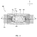
- FIG. 3 is a plan view of a photoelectron device 300 obtained by sealing the lead frame 100 of Embodiment 1 with a resin 302 so as to provide a resin package, mounting a photoelectron element 303 thereon, and cutting the lead frame into individual devices.
- the resin 302 is translucent so that the portion covered by the resin 302 can be shown explicitly in FIG. 3.
- FIG. 4 is a cross-sectional view taken along line IV-IV of FIG. 3 from the direction indicated by the arrow.
- a X-Y-Z rectangular coordinate system as shown in FIGS. 3 and 4 is used.
- the X axis direction corresponds to the rolling direction 150 in FIG. 1
- the Z axis direction corresponds to the vertical direction (thickness direction) of the resin package.
- the resin 302 is formed in a substantially rectangular solid shape, and the outer leads 103 are exposed from both end faces of the resin 302.
- An opening 307 is provided on the upper surface of the resin package, and the die pad 200, the connection portion 111 of the support lead 110 that is connected to the die pad 200, the end portions of the first inner leads 101, and the end portions of the second inner leads 102 are exposed in the opening.
- the upper surfaces of the metal portions such as the die pad 200 and the first inner leads 101 in the opening 307 are substantially flush with the upper surface of the resin 302 surrounding the metal portions.
- Such an opening 307 can be formed by performing the resin-sealing while placing a mold in a portion corresponding to the opening 307.
- the lower surface of the die pad main portion 203 of the die pad 200 is exposed in the lower surface of the resin package. Exposing a part of the die pad 200 allows efficient heat release for the photoelectron element 303 mounted on the die pad 200 via this exposed portion.
- the width of the die pad 200 in the shorter side direction (X axis direction) is D1
- the width of the die pad main portion 203 in the same direction is D2 (see FIG. 1).
- This stepwise change in thickness on the side of the longer side on the lower surface of the die pad 200 can increase an area that is in contact with the resin 302, so that the adhesiveness with the resin can be improved.
- the thickness in the X axis direction of the resin adhering on the side of the longer side of the die pad 200 can be small, so that the size of the resin package in the X axis direction can be reduced further.
- the portions having different thicknesses on the side of the longer side of the die pad 200 as above can be formed, for example, during rolling or the subsequent press stamping in the process of manufacturing the lead frame.
- the width of the opening 307 in the X axis direction is D3 in the portion of the the pad 200.
- the width D3 of the opening is smaller than the width D1 in the shorter side direction of the die pad 200. This allows the longer side portion of the die pad 200 to be fixed firmly with resin from the upper and lower directions.
- the difference between D1 and D3, namely, the overlapping width of the resin, can be suitably determined in view of the fixing strength of the die pad 200 and the opening width necessary for the opening 307.
- the width of the opening 307 in the X axis direction is D4 in the vicinity of the arranged end portions of the first inner leads 101.
- D4 is smaller than D3. This allows improved fixing strength of the end portions of first inner leads 101 and second inner leads 102, and the connection portion 111 of the support lead 110.
- the lengths of the portions of the first inner leads 101 and the second inner leads 102 that are exposed in the opening 307 are shorter than those of the portions sealed with the resin 302. Sealing most parts of the inner leads improves the fixing strength of the inner leads. Moreover, deformation of the end portions or peeling from the resin hardly occur. Furthermore, with respect to the outer lead side, resin-sealing is performed up to the portion having the same width (L3) and the same thickness (t0) as those of the outer leads 103. Thus, the outer leads 103 are fixed firmly.
- each lead exposed in the opening 307 is connected to the photoelectron element 303 by wiring. Therefore, the shape and the size of the opening 307 are designed so as to obtain peripheral space and regions necessary for this connection.
- connection portion 111 of the support lead 110 that is connected to the die pad 200 in such a manner that the connection portion 111 extends between the end portions of the inner leads 101 and the die pad 200, so as to expose the connection portion 111 in the opening 307 in the same manner that the end portions of the second inner leads 102 are exposed.
- This allows connection between the exposed connection portion 111 and the photoelectron element 303 by wiring. This makes it unnecessary to provide the necessary lead for reference potential setting such as a ground in the die pad 200, so that the size of the resin package in the X axis direction can be reduced further.
- the photoelectron element 303 includes a light-emitting device and a photoreceptor, although not shown in detail in the drawings.
- the light-emitting device irradiates an optical disk with a light beam, and reflected light therefrom is received by the photoreceptor.
- the electrodes of the photoelectron element 303 are connected to the leads exposed in the opening, such as the end portions of the first inner leads 101, by wiring (not shown), so as to establish electric connections. Thereafter, optical members (lens, hologram, transparent resin, etc.) are provided on the photoelectron element 303 to seal the opening 307.
Landscapes
- Lead Frames For Integrated Circuits (AREA)
- Led Device Packages (AREA)
Abstract
Description
Claims (22)
- A lead frame comprising:a die pad comprising a die pad main portion having a large thickness and a die pad peripheral portion having an intermediate thickness smaller than that of the die pad main portion, provided on at least one side of the die pad main portion;at least one support lead connected to the die pad; andat least two first inner leads having a small thickness smaller than that of the die pad peripheral portion, arranged such that end portions thereof are opposed to the die pad peripheral portion.
- The lead frame according to claim 1, further comprising a thin second inner lead having a thickness substantially the same as that of the first inner leads,wherein the second inner lead extends substantially in a same direction as the first inner leads, andan end portion of the second inner lead is positioned between the end portions of the first inner leads and the the pad peripheral portion.
- The lead frame according to claim 1, wherein first outer leads having a thickness and a width larger than those of the end portions of the first inner leads are provided continuously from the first inner leads.
- The lead frame according to claim 1, which is manufactured by processes including rolling.
- The lead frame according to claim 1, wherein an upper surface of the die pad, an upper surface of the support lead, and an upper surface of the first inner lead are on a substantially common plane.
- A lead frame comprising:a die pad comprising a die pad main portion having a large thickness;at least one support lead connected to the die pad; andat least three first inner leads having a small thickness smaller than that of the die pad main portion, arranged such that end portions thereof are opposed to at least one side of the die pad,wherein each first inner lead has a narrow portion having a small width and a wide portion having a width larger than that of the narrow portion, the narrow portion positioned on the die pad side, the wide portion positioned on a side opposite to the die pad,a connection point between the narrow portion and the wide portion of a central first inner lead of the at least three first inner leads is positioned farther from the die pad than connection points between the narrow portions and the wide portions of first inner leads adjacent to the central first inner lead, anda gap between the central first inner lead and the adjacent first inner leads is smaller in the narrow portion than in the wide portion.
- The lead frame according to claim 6, further comprising a thin second inner lead having a thickness substantially the same as that of the first inner leads,wherein the second inner lead extends substantially in a same direction as the first inner leads, andan end portion of the second inner lead is positioned between the end portions of the first inner leads and the die pad.
- The lead frame according to claim 7, wherein a plurality of the second inner leads are provided such that the first inner leads are interposed between the second inner leads.
- The lead frame according to claim 7, wherein an outer edge of the end portion of the second inner lead in a direction of a side of the die pad opposing the end portions of the first inner leads is positioned within a range defined by the width of the die pad in that direction.
- A lead frame comprising a belt-shaped thick region having a large thickness and a belt-shaped thin region having a thickness smaller than that of the thick region, these regions being parallel to each other,wherein a die pad is formed in the thick region, and leads are formed in the thin region, andthe leads extend in a direction substantially perpendicular to that of the belt-shaped regions.
- The lead frame according to claim 10, whereinthe lead includes a plurality of first inner leads,end portions of the first inner leads are opposed to the die pad, andboth widths and gaps of the first inner leads are smaller on the end portion side than on a side opposite thereto.
- The lead frame according to claim 10, wherein the thick region and the thin region are formed by rolling.
- The lead frame according to claim 10, further comprising at least one belt-shaped intermediate region having an intermediate thickness between the belt-shaped thick region and the belt-shape thin region in parallel,wherein the belt-shaped intermediate region is formed so that a change in thickness between the belt-shaped thick region and the belt-shape thin region occurs stepwise.
- The lead frame according to claim 10, wherein an upper surface of the thick region and an upper surface of the thin region are on a substantially common plane.
- A resin package comprising:a the pad comprising a the pad main portion having a large thickness and a die pad peripheral portion having an intermediate thickness smaller than that of the die pad main portion, provided on at least one side of the die pad main portion;at least one support lead connected to the die pad;at least two first inner leads having a small thickness smaller than that of the die pad peripheral portion, arranged such that end portions thereof are opposed to the the pad peripheral portion; anda resin for sealing the the pad, the support lead and the first inner leads for integration while exposing a part of an upper surface and a part of a lower surface of the die pad and upper surfaces of the end portions of the first inner leads.
- The resin package according to claim 15, wherein a length of a portion of the first inner leads covered with the resin is longer than a length of exposed portions of the first inner leads.
- The resin package according to claim 15, wherein upper and lower surfaces of at least a part of a side different from the side of the die pad to which the first inner leads are opposed is covered by the resin.
- The resin package according to claim 15, whereineach first inner lead has a narrow portion having a small width and a wide portion having a width larger than that of the narrow portion, the narrow portion positioned on the die pad side, and the wide portion positioned on a side opposite to the die pad,gaps between the first inner leads are wider in the wide portion than in the narrow portion, andat least the wide portion is covered with the resin.
- A resin package comprising:a die pad comprising a die pad main portion having a large thickness;at least one support lead connected to the die pad;at least three first inner leads having a small thickness smaller than that of the die pad main portion, arranged such that end portions thereof are opposed to at least one side of the die pad,a resin for sealing the die pad, the support lead and the first inner leads for integration while exposing a part of an upper surface and a part of a lower surface of the die pad and upper surfaces of the end portions of the first inner leads,wherein each first inner lead has a narrow portion having a small width and a wide portion having a width larger than that of the narrow portion, the narrow portion being positioned on the die pad side, the wide portion being positioned on a side opposite to the die pad,a connection point between the narrow portion and the wide portion of a central first inner lead of the at least three first inner leads is positioned farther from the die pad than connection points between the narrow portions and the wide portions of first inner leads adjacent to the central first inner lead, anda gap between the central first inner lead and the adjacent first inner leads is smaller in the narrow portion than in the wide portion.
- The resin package according to claim 19, whereinthe part of an upper surface of the die pad and the upper surfaces of the end portions of the first inner leads are exposed by forming an opening, anda width of the opening in a direction of a side of the die pad opposing the first inner leads is smaller on the end portion side of the first inner leads than on the die pad portion side.
- A photoelectron device comprising:the resin package according to claim 15 or 19;a photoelectron element mounted on an upper surface of the die pad; andan optically transparent member for sealing the photoelectron element.
- The photoelectron device according to claim 21, wherein the photoelectron element comprises a light source for emitting light with which a recording medium is irradiated, and a photoreceptor for receiving reflected light from the recording medium.
Applications Claiming Priority (2)
| Application Number | Priority Date | Filing Date | Title |
|---|---|---|---|
| JP25705099 | 1999-09-10 | ||
| JP25705099 | 1999-09-10 |
Publications (2)
| Publication Number | Publication Date |
|---|---|
| EP1083602A2 true EP1083602A2 (en) | 2001-03-14 |
| EP1083602A3 EP1083602A3 (en) | 2002-01-16 |
Family
ID=17301052
Family Applications (1)
| Application Number | Title | Priority Date | Filing Date |
|---|---|---|---|
| EP00119722A Withdrawn EP1083602A3 (en) | 1999-09-10 | 2000-09-09 | Lead frame and resin package and photoelectron device using the same |
Country Status (7)
| Country | Link |
|---|---|
| US (1) | US6501156B1 (en) |
| EP (1) | EP1083602A3 (en) |
| JP (1) | JP3461332B2 (en) |
| KR (1) | KR20010070069A (en) |
| CN (1) | CN1216424C (en) |
| SG (1) | SG105463A1 (en) |
| TW (1) | TW466713B (en) |
Cited By (4)
| Publication number | Priority date | Publication date | Assignee | Title |
|---|---|---|---|---|
| EP1473775A3 (en) * | 2003-04-28 | 2006-01-11 | Matsushita Electric Industrial Co., Ltd. | Method for producing solid-state imaging device |
| EP1494292A3 (en) * | 2003-07-01 | 2009-10-21 | Panasonic Corporation | Solid-state imaging device and method for manufacturing the same |
| EP2315263A4 (en) * | 2008-07-29 | 2014-08-20 | Nichia Corp | DEVICE EMITTING LIGHT |
| CN120916531A (en) * | 2025-10-09 | 2025-11-07 | 浙江晶科能源有限公司 | Photovoltaic cell, preparation method of photovoltaic cell and photovoltaic module |
Families Citing this family (36)
| Publication number | Priority date | Publication date | Assignee | Title |
|---|---|---|---|---|
| JP4417541B2 (en) * | 2000-10-23 | 2010-02-17 | ローム株式会社 | Semiconductor device and manufacturing method thereof |
| JP3879452B2 (en) * | 2001-07-23 | 2007-02-14 | 松下電器産業株式会社 | Resin-sealed semiconductor device and manufacturing method thereof |
| US7102216B1 (en) * | 2001-08-17 | 2006-09-05 | Amkor Technology, Inc. | Semiconductor package and leadframe with horizontal leads spaced in the vertical direction and method of making |
| JP3638136B2 (en) * | 2001-12-27 | 2005-04-13 | 株式会社三井ハイテック | Lead frame and semiconductor device using the same |
| JP4211359B2 (en) * | 2002-03-06 | 2009-01-21 | 日亜化学工業株式会社 | Manufacturing method of semiconductor device |
| CN100334721C (en) * | 2002-06-28 | 2007-08-29 | 矽品精密工业股份有限公司 | Flip Chip Semiconductor Package |
| KR100902766B1 (en) * | 2002-09-27 | 2009-06-15 | 페어차일드코리아반도체 주식회사 | Discrete Packages with Insulated Ceramic Heat Sink |
| CN100490140C (en) * | 2003-07-15 | 2009-05-20 | 飞思卡尔半导体公司 | Double gauge lead frame |
| JP4031748B2 (en) | 2003-10-06 | 2008-01-09 | ローム株式会社 | Semiconductor laser |
| US6867072B1 (en) | 2004-01-07 | 2005-03-15 | Freescale Semiconductor, Inc. | Flipchip QFN package and method therefor |
| TWI245399B (en) * | 2004-03-11 | 2005-12-11 | Advanced Semiconductor Eng | Leadframe with die pad |
| US7456499B2 (en) * | 2004-06-04 | 2008-11-25 | Cree, Inc. | Power light emitting die package with reflecting lens and the method of making the same |
| JP2007012857A (en) * | 2005-06-30 | 2007-01-18 | Renesas Technology Corp | Semiconductor device |
| WO2007037190A1 (en) * | 2005-09-27 | 2007-04-05 | Matsushita Electric Industrial Co., Ltd. | Heat dissipating wiring board, method for manufacturing same, and electric device using heat dissipating wiring board |
| US8174096B2 (en) * | 2006-08-25 | 2012-05-08 | Asm Assembly Materials Ltd. | Stamped leadframe and method of manufacture thereof |
| JP5089184B2 (en) | 2007-01-30 | 2012-12-05 | ローム株式会社 | Resin-sealed semiconductor device and manufacturing method thereof |
| JP5122172B2 (en) | 2007-03-30 | 2013-01-16 | ローム株式会社 | Semiconductor light emitting device |
| US8278148B2 (en) * | 2007-09-13 | 2012-10-02 | Stats Chippac Ltd. | Integrated circuit package system with leads separated from a die paddle |
| JP5416975B2 (en) | 2008-03-11 | 2014-02-12 | ローム株式会社 | Semiconductor light emitting device |
| US8158999B2 (en) * | 2008-03-14 | 2012-04-17 | Sung Jung Minute Industry Co., Ltd. | Reinforced chip package structure |
| US8716848B2 (en) * | 2008-03-24 | 2014-05-06 | SemiLEDs Optoelectronics Co., Ltd. | LED device with conductive wings and tabs |
| US8829685B2 (en) * | 2009-03-31 | 2014-09-09 | Semiconductor Components Industries, Llc | Circuit device having funnel shaped lead and method for manufacturing the same |
| TWI397139B (en) * | 2009-12-01 | 2013-05-21 | 萬國半導體有限公司 | Lead-exposed semiconductor package process |
| WO2011122665A1 (en) * | 2010-03-30 | 2011-10-06 | 大日本印刷株式会社 | Leadframe or substrate for led, semiconductor device, and method for manufacturing leadframe or substrate for led |
| JP2012028699A (en) * | 2010-07-27 | 2012-02-09 | Panasonic Corp | Semiconductor device, lead frame assembly and manufacturing method of the same |
| US8933548B2 (en) * | 2010-11-02 | 2015-01-13 | Dai Nippon Printing Co., Ltd. | Lead frame for mounting LED elements, lead frame with resin, method for manufacturing semiconductor devices, and lead frame for mounting semiconductor elements |
| JP2012113919A (en) * | 2010-11-24 | 2012-06-14 | Toshiba Corp | Lighting device |
| DE102012215449A1 (en) * | 2012-08-31 | 2014-03-27 | Osram Opto Semiconductors Gmbh | HOUSING FOR AN ELECTRONIC COMPONENT, ELECTRONIC MODULE, METHOD FOR MANUFACTURING A HOUSING FOR AN ELECTRONIC COMPONENT AND METHOD FOR PRODUCING AN ELECTRONIC MODULE |
| JP2014073517A (en) * | 2012-10-04 | 2014-04-24 | Denso Corp | Method of manufacturing metal piece |
| CN103178041B (en) * | 2013-03-27 | 2016-05-04 | 日月光封装测试(上海)有限公司 | Lead frame moulding and glue sealing method |
| US9082760B2 (en) * | 2014-06-16 | 2015-07-14 | Chang Wah Technology Co., Ltd. | Dual layered lead frame |
| US9418920B2 (en) | 2015-01-05 | 2016-08-16 | Stmicroelectronics Pte Ltd | Integrated circuit (IC) package with thick die pad functioning as a heat sink |
| US10083899B2 (en) * | 2017-01-23 | 2018-09-25 | Infineon Technologies Ag | Semiconductor package with heat slug and rivet free die attach area |
| DE102017102700A1 (en) | 2017-02-10 | 2018-09-13 | Atg Luther & Maelzer Gmbh | Test apparatus and method for testing printed circuit boards |
| US12368054B2 (en) * | 2020-01-09 | 2025-07-22 | Texas Instruments Incorporated | Lead frame rolling |
| US11747273B2 (en) * | 2020-09-28 | 2023-09-05 | Asahi Kasei Microdevices Corporation | Gas sensor |
Family Cites Families (22)
| Publication number | Priority date | Publication date | Assignee | Title |
|---|---|---|---|---|
| JPS53126268A (en) | 1977-04-11 | 1978-11-04 | Hitachi Ltd | Semiconductor device |
| JPH01106456A (en) | 1987-10-19 | 1989-04-24 | Matsushita Electric Ind Co Ltd | Semiconductor integrated circuit device |
| JPH01150347A (en) | 1987-12-07 | 1989-06-13 | Nec Corp | Lead frame for manufacture of semiconductor device |
| JPH0824157B2 (en) | 1989-08-01 | 1996-03-06 | 株式会社三井ハイテック | Method for manufacturing semiconductor device |
| JPH03147358A (en) | 1989-11-02 | 1991-06-24 | Nec Corp | Lead frame |
| JP2533012B2 (en) | 1991-06-27 | 1996-09-11 | 三洋電機株式会社 | Surface mount semiconductor device |
| US5451813A (en) | 1991-09-05 | 1995-09-19 | Rohm Co., Ltd. | Semiconductor device with lead frame having different thicknesses |
| JPH05326788A (en) | 1992-05-25 | 1993-12-10 | Nippon Steel Corp | Lead frame material and semiconductor device using the same |
| JPH06203403A (en) | 1992-10-22 | 1994-07-22 | Matsushita Electron Corp | Semiconductor laser device and optical pickup device |
| JPH06196603A (en) * | 1992-12-23 | 1994-07-15 | Shinko Electric Ind Co Ltd | Manufacture of lead frame |
| US5454905A (en) * | 1994-08-09 | 1995-10-03 | National Semiconductor Corporation | Method for manufacturing fine pitch lead frame |
| EP0790652B1 (en) | 1995-08-02 | 2007-02-21 | Matsushita Electric Industrial Co., Ltd. | Solid-state image pickup device and its manufacture |
| JP3012816B2 (en) * | 1996-10-22 | 2000-02-28 | 松下電子工業株式会社 | Resin-sealed semiconductor device and method of manufacturing the same |
| TW351008B (en) * | 1996-12-24 | 1999-01-21 | Matsushita Electronics Corp | Lead holder, manufacturing method of lead holder, semiconductor and manufacturing method of semiconductor |
| EP0895287A3 (en) * | 1997-07-31 | 2006-04-05 | Matsushita Electric Industrial Co., Ltd. | Semiconductor device and lead frame for the same |
| JP3285815B2 (en) * | 1998-03-12 | 2002-05-27 | 松下電器産業株式会社 | Lead frame, resin-encapsulated semiconductor device and method of manufacturing the same |
| JP3562311B2 (en) * | 1998-05-27 | 2004-09-08 | 松下電器産業株式会社 | Method for manufacturing lead frame and resin-encapsulated semiconductor device |
| US6229200B1 (en) * | 1998-06-10 | 2001-05-08 | Asat Limited | Saw-singulated leadless plastic chip carrier |
| US6143981A (en) * | 1998-06-24 | 2000-11-07 | Amkor Technology, Inc. | Plastic integrated circuit package and method and leadframe for making the package |
| US6281568B1 (en) * | 1998-10-21 | 2001-08-28 | Amkor Technology, Inc. | Plastic integrated circuit device package and leadframe having partially undercut leads and die pad |
| US6208020B1 (en) * | 1999-02-24 | 2001-03-27 | Matsushita Electronics Corporation | Leadframe for use in manufacturing a resin-molded semiconductor device |
| US6274927B1 (en) * | 1999-06-03 | 2001-08-14 | Amkor Technology, Inc. | Plastic package for an optical integrated circuit device and method of making |
-
2000
- 2000-09-04 JP JP2000266601A patent/JP3461332B2/en not_active Expired - Fee Related
- 2000-09-05 TW TW089118131A patent/TW466713B/en not_active IP Right Cessation
- 2000-09-08 US US09/657,484 patent/US6501156B1/en not_active Expired - Lifetime
- 2000-09-08 SG SG200005123A patent/SG105463A1/en unknown
- 2000-09-09 EP EP00119722A patent/EP1083602A3/en not_active Withdrawn
- 2000-09-09 KR KR1020000053820A patent/KR20010070069A/en not_active Ceased
- 2000-09-11 CN CN001270214A patent/CN1216424C/en not_active Expired - Lifetime
Cited By (4)
| Publication number | Priority date | Publication date | Assignee | Title |
|---|---|---|---|---|
| EP1473775A3 (en) * | 2003-04-28 | 2006-01-11 | Matsushita Electric Industrial Co., Ltd. | Method for producing solid-state imaging device |
| EP1494292A3 (en) * | 2003-07-01 | 2009-10-21 | Panasonic Corporation | Solid-state imaging device and method for manufacturing the same |
| EP2315263A4 (en) * | 2008-07-29 | 2014-08-20 | Nichia Corp | DEVICE EMITTING LIGHT |
| CN120916531A (en) * | 2025-10-09 | 2025-11-07 | 浙江晶科能源有限公司 | Photovoltaic cell, preparation method of photovoltaic cell and photovoltaic module |
Also Published As
| Publication number | Publication date |
|---|---|
| KR20010070069A (en) | 2001-07-25 |
| JP2001148456A (en) | 2001-05-29 |
| CN1288261A (en) | 2001-03-21 |
| JP3461332B2 (en) | 2003-10-27 |
| SG105463A1 (en) | 2004-08-27 |
| CN1216424C (en) | 2005-08-24 |
| TW466713B (en) | 2001-12-01 |
| US6501156B1 (en) | 2002-12-31 |
| EP1083602A3 (en) | 2002-01-16 |
Similar Documents
| Publication | Publication Date | Title |
|---|---|---|
| US6501156B1 (en) | Lead frame which includes a die pad, a support lead, and inner leads | |
| CN100459136C (en) | Solid-state imaging device and manufacturing method thereof | |
| JP3782406B2 (en) | Solid-state imaging device and manufacturing method thereof | |
| US7273765B2 (en) | Solid-state imaging device and method for producing the same | |
| US20150003077A1 (en) | Light emitting device | |
| US20090290054A1 (en) | Solid-state imaging device | |
| JP3999780B2 (en) | Lead frame manufacturing method | |
| CN101064763B (en) | Image sensor and manufacturing method thereof | |
| JP2003179292A (en) | Semiconductor laser device and method of manufacturing the same | |
| KR100691178B1 (en) | Side light emitting diode with light emitting diode chip placed behind the lead frame | |
| JP2004104153A (en) | Light emitting element and semiconductor device | |
| JPH08293756A (en) | Surface acoustic wave device package | |
| CN1533003A (en) | semiconductor laser device | |
| JPS59178757A (en) | Lead frame | |
| JPH11102998A (en) | Package for electronic component | |
| CN120376978A (en) | Optical drive base and preparation method | |
| JPS5824020B2 (en) | semiconductor equipment | |
| CN112904618A (en) | Backlight module and light guide plate manufacturing method | |
| KR100378277B1 (en) | A semiconductor device | |
| KR100379094B1 (en) | A structure and manufacturing method of the lead frame for semiconductor packages | |
| JP2000083138A (en) | Image reader and light emitting element array for the same | |
| JP2021162660A (en) | Optical waveguide module and light source module | |
| JPH0982849A (en) | Heat sink for semiconductor package | |
| JPH03290937A (en) | Bumped metallic lead and its manufacture | |
| JPS6347272B2 (en) |
Legal Events
| Date | Code | Title | Description |
|---|---|---|---|
| PUAI | Public reference made under article 153(3) epc to a published international application that has entered the european phase |
Free format text: ORIGINAL CODE: 0009012 |
|
| AK | Designated contracting states |
Kind code of ref document: A2 Designated state(s): AT BE CH CY DE DK ES FI FR GB GR IE IT LI LU MC NL PT SE Kind code of ref document: A2 Designated state(s): DE FR GB |
|
| AX | Request for extension of the european patent |
Free format text: AL;LT;LV;MK;RO;SI |
|
| RAP1 | Party data changed (applicant data changed or rights of an application transferred) |
Owner name: MATSUSHITA ELECTRIC INDUSTRIAL CO., LTD. |
|
| PUAL | Search report despatched |
Free format text: ORIGINAL CODE: 0009013 |
|
| AK | Designated contracting states |
Kind code of ref document: A3 Designated state(s): AT BE CH CY DE DK ES FI FR GB GR IE IT LI LU MC NL PT SE |
|
| AX | Request for extension of the european patent |
Free format text: AL;LT;LV;MK;RO;SI |
|
| RIC1 | Information provided on ipc code assigned before grant |
Free format text: 7H 01L 23/495 A, 7H 01L 31/02 B, 7H 01L 33/00 B, 7H 01L 23/48 B, 7H 01L 23/50 B |
|
| 17P | Request for examination filed |
Effective date: 20011221 |
|
| AKX | Designation fees paid |
Free format text: DE FR GB |
|
| 17Q | First examination report despatched |
Effective date: 20040615 |
|
| RAP1 | Party data changed (applicant data changed or rights of an application transferred) |
Owner name: PANASONIC CORPORATION |
|
| RTI1 | Title (correction) |
Free format text: LEAD FRAME AND RESIN PACKAGE AND OPTOELECTRONIC DEVICE USING THE SAME |
|
| STAA | Information on the status of an ep patent application or granted ep patent |
Free format text: STATUS: THE APPLICATION IS DEEMED TO BE WITHDRAWN |
|
| 18D | Application deemed to be withdrawn |
Effective date: 20100309 |