EP1083597A2 - Vefahren zur Herstellung einer kontrollierbaren und reproduzierbaren Kupfer-Doppeldamaszen-Struktur - Google Patents
Vefahren zur Herstellung einer kontrollierbaren und reproduzierbaren Kupfer-Doppeldamaszen-Struktur Download PDFInfo
- Publication number
- EP1083597A2 EP1083597A2 EP00640008A EP00640008A EP1083597A2 EP 1083597 A2 EP1083597 A2 EP 1083597A2 EP 00640008 A EP00640008 A EP 00640008A EP 00640008 A EP00640008 A EP 00640008A EP 1083597 A2 EP1083597 A2 EP 1083597A2
- Authority
- EP
- European Patent Office
- Prior art keywords
- layer
- spin
- copper
- dual damascene
- dielectric
- Prior art date
- Legal status (The legal status is an assumption and is not a legal conclusion. Google has not performed a legal analysis and makes no representation as to the accuracy of the status listed.)
- Withdrawn
Links
Images


Classifications
-
- H—ELECTRICITY
- H01—ELECTRIC ELEMENTS
- H01L—SEMICONDUCTOR DEVICES NOT COVERED BY CLASS H10
- H01L21/00—Processes or apparatus adapted for the manufacture or treatment of semiconductor or solid state devices or of parts thereof
- H01L21/70—Manufacture or treatment of devices consisting of a plurality of solid state components formed in or on a common substrate or of parts thereof; Manufacture of integrated circuit devices or of parts thereof
- H01L21/71—Manufacture of specific parts of devices defined in group H01L21/70
- H01L21/768—Applying interconnections to be used for carrying current between separate components within a device comprising conductors and dielectrics
- H01L21/76838—Applying interconnections to be used for carrying current between separate components within a device comprising conductors and dielectrics characterised by the formation and the after-treatment of the conductors
- H01L21/76841—Barrier, adhesion or liner layers
- H01L21/76843—Barrier, adhesion or liner layers formed in openings in a dielectric
-
- H—ELECTRICITY
- H01—ELECTRIC ELEMENTS
- H01L—SEMICONDUCTOR DEVICES NOT COVERED BY CLASS H10
- H01L21/00—Processes or apparatus adapted for the manufacture or treatment of semiconductor or solid state devices or of parts thereof
- H01L21/70—Manufacture or treatment of devices consisting of a plurality of solid state components formed in or on a common substrate or of parts thereof; Manufacture of integrated circuit devices or of parts thereof
- H01L21/71—Manufacture of specific parts of devices defined in group H01L21/70
- H01L21/768—Applying interconnections to be used for carrying current between separate components within a device comprising conductors and dielectrics
- H01L21/76838—Applying interconnections to be used for carrying current between separate components within a device comprising conductors and dielectrics characterised by the formation and the after-treatment of the conductors
- H01L21/7684—Smoothing; Planarisation
-
- H—ELECTRICITY
- H01—ELECTRIC ELEMENTS
- H01L—SEMICONDUCTOR DEVICES NOT COVERED BY CLASS H10
- H01L21/00—Processes or apparatus adapted for the manufacture or treatment of semiconductor or solid state devices or of parts thereof
- H01L21/70—Manufacture or treatment of devices consisting of a plurality of solid state components formed in or on a common substrate or of parts thereof; Manufacture of integrated circuit devices or of parts thereof
- H01L21/71—Manufacture of specific parts of devices defined in group H01L21/70
- H01L21/768—Applying interconnections to be used for carrying current between separate components within a device comprising conductors and dielectrics
- H01L21/76838—Applying interconnections to be used for carrying current between separate components within a device comprising conductors and dielectrics characterised by the formation and the after-treatment of the conductors
- H01L21/76841—Barrier, adhesion or liner layers
- H01L21/76871—Layers specifically deposited to enhance or enable the nucleation of further layers, i.e. seed layers
- H01L21/76874—Layers specifically deposited to enhance or enable the nucleation of further layers, i.e. seed layers for electroless plating
-
- H—ELECTRICITY
- H01—ELECTRIC ELEMENTS
- H01L—SEMICONDUCTOR DEVICES NOT COVERED BY CLASS H10
- H01L21/00—Processes or apparatus adapted for the manufacture or treatment of semiconductor or solid state devices or of parts thereof
- H01L21/70—Manufacture or treatment of devices consisting of a plurality of solid state components formed in or on a common substrate or of parts thereof; Manufacture of integrated circuit devices or of parts thereof
- H01L21/71—Manufacture of specific parts of devices defined in group H01L21/70
- H01L21/768—Applying interconnections to be used for carrying current between separate components within a device comprising conductors and dielectrics
- H01L21/76838—Applying interconnections to be used for carrying current between separate components within a device comprising conductors and dielectrics characterised by the formation and the after-treatment of the conductors
- H01L21/76841—Barrier, adhesion or liner layers
- H01L21/76871—Layers specifically deposited to enhance or enable the nucleation of further layers, i.e. seed layers
- H01L21/76876—Layers specifically deposited to enhance or enable the nucleation of further layers, i.e. seed layers for deposition from the gas phase, e.g. CVD
-
- H—ELECTRICITY
- H01—ELECTRIC ELEMENTS
- H01L—SEMICONDUCTOR DEVICES NOT COVERED BY CLASS H10
- H01L21/00—Processes or apparatus adapted for the manufacture or treatment of semiconductor or solid state devices or of parts thereof
- H01L21/70—Manufacture or treatment of devices consisting of a plurality of solid state components formed in or on a common substrate or of parts thereof; Manufacture of integrated circuit devices or of parts thereof
- H01L21/71—Manufacture of specific parts of devices defined in group H01L21/70
- H01L21/768—Applying interconnections to be used for carrying current between separate components within a device comprising conductors and dielectrics
- H01L21/76838—Applying interconnections to be used for carrying current between separate components within a device comprising conductors and dielectrics characterised by the formation and the after-treatment of the conductors
- H01L21/76877—Filling of holes, grooves or trenches, e.g. vias, with conductive material
- H01L21/76879—Filling of holes, grooves or trenches, e.g. vias, with conductive material by selective deposition of conductive material in the vias, e.g. selective C.V.D. on semiconductor material, plating
Definitions
- the invention relates to the fabrication of integrated circuit devices, and more particularly, to a method for reducing dishing and erosion effects in the copper surface of copper dual damascene structures.
- the first or lowest level of interconnect wires is typically formed as a first step in the process after which a second or overlying level of interconnect wires is deposited over the first level.
- the first level of interconnect wires is typically in contact with active regions in a semiconductor substrate but is not limited to such contact.
- the first level of interconnect can for instance also be in contact with a conductor that leads to other devices that form part of a larger, multi-chip structure.
- the two levels of metal wires are connected by openings between the two layers that are filled with metal where the openings between the two layers are lines up with and match contact points in one or both of the levels of metal lines.
- Previously used techniques to form multi-levels of wiring apply the technique of first forming the interconnect level metal in a first plane followed by forming the overlying level of interconnect wire in a second plane.
- This structure typically starts with the surface of a semiconductor substrate into which active devices have been created. These active devices can include bipolar transistors, MOSFET devices, doped regions that interconnect with other regions of the device while provisions may also have been provided to make interconnects with I/O terminals in the periphery of the device.
- the surface into which the pattern of interconnect lines of the first plane is formed may also be an insulation layer deposited over the surface of the substrate or a layer of oxide may first have been formed on the surface of the substrate.
- the interconnecting pattern itself needs to be defined. This is done using conventional photolithographic techniques whereby the openings are made (in the layer) above the points that need to be contacted in the substrate.
- the openings, once created, may by lined with layers of material to enhance metal adhesion (to the sidewalls of the opening), the glue layer, or to prevent diffusion of materials into and from the substrate in subsequent processing steps, the barrier layer.
- the barrier layer a variety of materials can be used such as Ti/Tin:W (titanium/titanium nitride:tungsten), titaniumtungsten/titanium or titanium-tungsten nitride/titanium or titanium nitride or titamium nitride/titanium, silicon nitride (Si3N4), tungsten, tantalum, niobium, molybdenum.
- the final phase in creating the first level of interconnect lines is to fill the created openings with metal, typically aluminum, tungsten or copper, dependent on the particular application and requirements and restrictions imposed by such parameters as line width, aspect ratio of the opening, required planarity of the surface of the deposited metal and others.
- This process of line formation in overlying layers on metal can be repeated in essentially the same manner as just highlighted for the first layer of interconnecting wires.
- This process of forming sequential layers of interconnecting levels of wire is in many instances prone to problems and limitations. Copper has in recent times found more application in the use of metal wires due to its low resistivity, high electromigration resistance and stress voiding resistance. Copper however exhibits the disadvantage of high diffusivity in common insulating materials such as silicon dioxide and oxygen-containing polymers. This leads to, for instance, the diffusion of copper into polyimide during high temperature processing of the polyimide resulting in severe erosion of the copper and the polyimide due to the copper combining with oxygen in the polyimide.
- the erosion may result in loss of adhesion, delamination, voids, and ultimately a catastrophic failure of the component.
- the copper that is used in an interconnect may diffuse into the silicon dioxide layer causing the dielectric strength to become conductive and also decreasing the dielectric strength of the silicon dioxide layer.
- a copper diffusion barrier is therefore often required; silicon nitride is often applied as a diffusion barrier to copper. Silicon nitride however has a dielectric constant that is high compared to silicon dioxide thereby limiting the use of silicon nitride in encapsulating copper interconnect lines.
- the CMP method may need to be used where copper is used as a wiring material.
- the copper etch rate must be raised by increasing the amount of the component responsible for copper etching contained in the polishing slurry. If the component is used in an increased amount, the etching will occur isotropically. Consequently, buried copper is etched away, causing dishing in the wiring. It is, when forming interconnect lines using copper, desirable to use methods that do not depend on patterning the copper lines using a chemical etching process since etching of copper is very difficult and is a process that is only recently being further investigated.
- copper as a metal for interconnect wiring is further hindered by copper's susceptibility to oxidation.
- Conventional photoresist processing cannot be used when the copper is to be patterned into various wire shapes because the photoresist needs to be removed at the end of the process by heating it in a highly oxidized environment, such as an oxygen plasma, thereby converting it to an easily removed ash.
- a metal plug is first formed in a surface; this surface in most instances is the surface of a semiconductor substrate.
- a layer of Intra Level Dielectric (ILD) is deposited (using for instance Plasma Enhanced CVD technology with SiO 2 as a dielectric) over the surface into which trenches for metal lines are formed (using for instance Reactive Ion Etching technology).
- ILD Intra Level Dielectric
- the trenches overlay the metal plug and are filled with metal (using for instance either the CVD or a metal flow process). Planarization of this metal to the top surface of the layer of ILD completes the damascene structure.
- Some early damascene structures have been achieved using Reactive Ion Etching (RIE) for the process of planarization but Chemical Mechanical Planarization (CMP) is used exclusively today.
- RIE Reactive Ion Etching
- CMP Chemical Mechanical Planarization
- Damascene is an interconnection fabrication process in which grooves are formed in an insulating layer and filled with metal to form the conductive lines.
- Dual damascene is a multi-level interconnection process in which, in-addition to forming the grooves of single damascene, conductive via openings also are formed.
- One of the dual damascene approaches uses a dielectric layer that is formed by three consecutive depositions whereby the central layer functions as an etch stop layer.
- This etch stop layer can be SiN, the top and bottom layer of this three layer configuration can be SiO 2 .
- This triple layer dielectric allows first forming the vias by resist patterning the vias and etching through the three layers of dielectric. The conductive pattern can then be formed in the top layer of dielectric whereby the central layer of SiN forms the stop layer for the etch of the conducting pattern.
- Another approach, still using the three-layer dielectric formed on the substrate surface, is to first form the pattern for the conducting lines in the top layer of the dielectric whereby the SiN layer again serves as etch stop. The vias can then be formed by aligning the via pattern with the pattern of the conducting lines and patterning and etching the vias through the etch stop layer of SiN and the first layer of dielectric.
- Yet another approach is to deposit the three layer dielectric in two steps, first depositing the first layer of SiO 2 and the etch stop layer of SiN. At this point the via pattern can be exposed and etched. The top layer of SiO 2 dielectric is then deposited; the conducting lines are now patterned and etched. The SiN layer will stop the etching except where the via openings have already been etched.
- Dual damascene is an improvement over single damascene because it permits the filling of both the conductive grooves and vias with metal at the same time, thereby eliminating processing steps.
- Some of the problems encountered in creating the dual damascene structure relate to the fact that the depth of the interconnect channels is difficult to control due to non-uniform film deposition and the precise control of etch rates during the process of etching the interconnect pattern. This can result in interconnect line profiles that are not uniform across the wafer with deeper line profiles in the center of the wafer and shallower line profiles toward the periphery of the wafer. For smaller device feature holes are required that have small aspect ratios making the filling of the holes with sputtering very difficult.
- the metals that are typically used for interconnect lines such as aluminum, copper, gold and silver, can not readily be deposited using CVD technology even though this latter technology does provide better depth of penetration.
- CVD technology For materials where CYD can be used for their deposition such as polysilicon and tungsten, these material exhibit higher resistivity as compared to aluminum, copper, gold and silver.
- the invention provides a method to reduce the indicated dishing and erosion in the surface of the polished copper thereby improving planarity and uniformity of copper trenches in large and small device features.
- the invention teaches a method of forming a Cu seed layer over the surface of the Inter Metal Dielectric (IMD) and inside the dual damascene opening, filling the dual damascene opening with a spin-on material such as SOG, etching the seed layer above the IMD, removing the spin-on material, and completing the dual damascene structure with an electroless deposition of Cu in the dual damascene opening.
- a spin-on material such as SOG
- US 5,705,430 shows a dual damascene process with a sacrificial via fill.
- a principle objective of the invention is to reduce surface dishing and erosion in the copper surface of a dual damascene structure.
- Another objective of the invention is to improve global planarity and uniformity of the copper surfaces of dual damascene structures.
- a new method for creating a dual damascene structure.
- a layer of IMD is first deposited over the surface of a substrate.
- a cap layer is deposited over this layer of IMD, the dual damascene structure (having a via and a trench opening) is then patterned through the cap layer and into the layer of IMD.
- a tantalum or tungsten or titanium based barrier layer is deposited in the dual damascene structure and over the surface of the cap layer, a copper seed layer is further deposited over the barrier layer.
- the dual damascene structure is then filled with a spin on material; this spin on material can be fully or partially cured.
- the tantalum or tungsten or titanium based barrier layer and the copper seed layer are removed above the layer of IMD; the cap layer can be partially removed above the layer of IMD or can be left in place.
- the spin on material remains in place in the via and trench opening of the dual damascene structure during the latter operation thereby protecting the inside surfaces of these openings during the latter process (of removing the copper seed and the Ta or W or Ti based barrier layer from above the surface of the IMD.
- the spin-on material is next removed and copper is deposited by selective electroless plating.
- the cap layer that is still (at least partially) present above the surface of the IMD now protects the IMD dielectric from being contaminated with copper solution during the selective electroless deposition of the copper.
- the excess copper is removed above the surface of the IMD by a touch-up CMP.
- the cap layer on the surface of the IMD can, after the copper has been deposited, be removed if this is so desired.
- a liner or oxidation/diffusion protection layer is deposited over the dual damascene structure and its surrounding area.
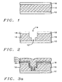
- Fig. 1 shows a cross section of a metal surface with a layer of IMD and a cap layer deposited over the layer of metal.
- Fig. 2 shows a cross section of the dual damascene structure formed through the cap layer and in the layer of IMD.
- Fig. 3a shows a cross section after the deposition of a barrier layer, a copper seed layer and a resist spin-on material over the dual damascene profile and its surrounding cap layer.
- Fig. 3b shows the cross section of Fig. 3a after the removal of the excess resist spin-on material.
- Fig. 4a shows a cross section after the deposition of a barrier layer, a copper seed layer and a SOG or polyimide spinon material over the dual damascene profile and its surrounding cap layer.
- Fig. 4b shows the cross section of Fig. 4a after the barrier layer, the copper seed layer and the spin-on material have been removed from above the surface of the surrounding cap layer (above the IMD).
- Fig. 5 shows a cross section of the dual damascene structure after selective electroless deposition of copper over the dual damascene structure.
- Fig. 6 shows a cross section after the excess copper has been removed from the surface of the surrounding cap layer by a touch-up CMP.
- Fig. 7 shows a cross section after the final deposition of an oxidation/diffusion protection layer.
- FIG. 1 there is shown a cross section of a metal surface 10 over which a layer 16 of Inter Metal dielectric (IMD) has been deposited.
- IMD Inter Metal dielectric
- the requirements for the cap layer are essentially the same as the requirements for a typical copper barrier layer with the understanding that it can be readily removed from the surface of the IMD by either an etch or CMP.
- a further requirement is that the cap layer be deposited to an adequate thickness, for instance between about 100 and 3000 Angstrom, so that this layer can provide its basic function of protecting the surface of the IMD during subsequent processing steps.
- the functions of the barrier layer and the copper seed layer have previously been highlighted. That is the copper seed layer serves to promote the selective electroless deposition of copper while the barrier layer prevents diffusion of materials between the dual damascene structure and its adjacent areas during subsequent processing steps.
- Fig. 2 shows a cross section of a dual damascene structure that has been formed through the cap layer 18 and in layer 16 of Inter Metal Dielectric (IMD).
- the dual damascene structure consists of the via part 12 that is in direct contact with the underlying layer of metal 10 and the interconnect line (or trench) part 14 that overlays the via structure 12.
- Figs. 3a and 3b address the case where the spin-on material is resist while Figs. 4a and 4b address the case where the spin-on material is SOG or polyimide.
- Fig. 3a shows a cross section of the dual damascene structure after the deposition of a barrier layer 20 over which a copper seed layer 22 has been deposited.
- a spin-on material 24 comprising resist is then deposited over the copper seed layer 22.
- Barrier layer 20 is deposited over the sidewalls of the dual damascene and over the surface of the cap layer 18 above the layer 16 of IMD, barrier layer 20 contains a tantalum or tungsten or titanium based material.
- the copper seed layer 22 is deposited over the barrier layer 20.
- the resist spin-on material 24 is used to fill the complete profile of the dual damascene structure, that is the via part 12 (Fig. 2) and the interconnect line part 14 (Fig. 2).
- Other spin-on materials can be Spin On Glass (SOG) or polyimide; these latter two spin-on materials are discussed under Figs. 4a and 4b following.
- the spin-on material may, during subsequent processing, be partially or completely cured.
- the function of the spin-on material is to protect the inside surfaces of the dual damascene structure during subsequent processing steps.
- Fig. 3a and 3b reflect that, if the spin-on material 24 is resist, the excess spin-on material 24 on the Cu seed layer 22 and above the layer of IMD (that surrounds the dual damascene opening) is etched away by a plasma dry etch, the plasma can be O 2 or H 2 based. After this, the copper seed layer 22 and the barrier layer 20 can be removed by an anisotropic dry etch (using a C1 or F-based plasma) with an overetch into cap layer 18. Because resist has high resistance to dry etch, resist 24 protects the underlying copper seed layer 22.
- An other method is to use DMSO/CCl 4 or HF/CH 3 COOH to selectively wet etch copper seed layer 22 while HF can selectively etch the tantalum/tungsten/titanium barrier layer 20 without etching much of the resist that is present over the dual damascene structure.
- Figs. 4a and 4b address the application where the spin-on material is SOG and polyimide.
- the excess spin-on material 24 above the layer 16 of IMD, the copper seed layer 22 and the barrier layer 20 are removed using CMP.
- the CMP process can be stopped after over-polish into cap layer 18.
- Fig. 4a shows a cross section of the dual damascene structure after the tantalum or tungsten or titanium barrier layer 20 (Fig. 4a), the copper seed layer 22 (Fig. 4a) and the SOG or polyimide based spin-on material 24 (Fig. 4a) have been removed above the cap layer 18.
- the spin-on material 24, Fig. 4b remains in place inside the opening of the dual damascene structure.
- the spin-on material 24 in this manner provides protection of the copper seed layer 22 inside the dual damascene structure and leaves this seed layer 22 essentially in place.
- the spin-on material 24 is removed from the inside of the opening as a separate processing step.
- the first entry (row) in column #2 for the resist spin-on material (highlighted with 1) relates to the removal of the excess spin-on material above the copper seed layer
- the second entry in column #2 for the resist spin-on material (highlighted with 2) relates to the removal of the copper seed and the barrier layers.
- the processing conditions for the removal of the resist spin-on material above the dual damascene structure is a dry etch (as shown in the table above), the temperature is between about 150 and 300 degrees C., the etchants used have been indicated in the table above, the flow rate is between about 10 and 3000 SCCM with a pressure between about 50 and 10000 mTORR while the time of the process of removal is between about 1 and 5 minutes.
- the processing conditions are as follows: the process is a dry etch for the removal of resist and polyimide (as shown in the table above), the temperature is between about 150 and 300 degrees C., the etchant used has been indicated in the table above as H 2 , the flow rate is between about 10 and 3000 SCCM with a pressure between about 50 and 10000 mTORR while the time of the process of removal is between about 1 second and 5 minutes.
- the cap layer 18 is still (at least partially) present above the layer of IMD. This presence of the cap layer 18 above the layer of IMD protects the IMD during the subsequent processing step of filling the dual damascene structure with copper.
- Fig. 5 shows a cross section of the dual damascene structure after the selective electroless deposition of a layer 26 of copper inside the opening for the dual damascene structure.
- the cap layer 18 is in place thereby protecting the surface of the IMD from being contaminated by the copper solution during the plating process.
- the process of filling the dual damascene structure with copper is an electroless plating process. Electroplating cannot be used for this application since a blanket copper film will form using this method. Selective CVD can also be used for the process of depositing the copper although this approach has as yet not found wide application.
- selective electroless deposition of copper into the dual damascene structure there is no copper deposition on the area above the IMD that surrounds the dual damascene opening while the copper plug will extend above the surface of the field area, see Fig. 5.
- a simply touch-up CMP the whole surface will be planarized resulting in a structure as shown in Fig. 6. Dishing or erosion has in this manner been eliminated. Electroplating cannot be used in this case since there is no continuous copper seed layer that can conduct the current.
- Fig. 6 shows a cross section after the excess copper has been removed from above the surface of the cap layer 18 down to the level of the top plane of the dual damascene structure 26 by a touch-up CMP.
- Fig. 7 shows the completion of the dual damascene structure of the invention by the deposition of a layer 30 that serves as a liner and/or copper oxidation/diffusion barrier layer.
- This layer 30 has been deposited over the cap layer 18, layer 30 serves as a final protective layer for the underlying structure.
- the liner 30 may contain Si3N4; layer 30 is typically deposited over the entire surface of the substrate.
- the cross section as shown in Fig. 7 indicates an application where the cap layer has been lowered (by partial removal) to below the surface of the copper 26 of the dual damascene structure.
- the layer 30 in this manner covers both the surface of the copper 26 and overlays the cap layer 18.
- dishing and erosion are due to the high polishing rate of copper as compared to that polishing rate of the barrier metal. With the structure as shown in Fig. 5, in which the copper plug is above the field area, dishing and erosion will not occur.
Landscapes
- Engineering & Computer Science (AREA)
- Physics & Mathematics (AREA)
- Condensed Matter Physics & Semiconductors (AREA)
- General Physics & Mathematics (AREA)
- Manufacturing & Machinery (AREA)
- Computer Hardware Design (AREA)
- Microelectronics & Electronic Packaging (AREA)
- Power Engineering (AREA)
- Internal Circuitry In Semiconductor Integrated Circuit Devices (AREA)
Applications Claiming Priority (2)
| Application Number | Priority Date | Filing Date | Title |
|---|---|---|---|
| US390782 | 1999-09-07 | ||
| US09/390,782 US6184138B1 (en) | 1999-09-07 | 1999-09-07 | Method to create a controllable and reproducible dual copper damascene structure |
Publications (2)
| Publication Number | Publication Date |
|---|---|
| EP1083597A2 true EP1083597A2 (de) | 2001-03-14 |
| EP1083597A3 EP1083597A3 (de) | 2003-06-18 |
Family
ID=23543915
Family Applications (1)
| Application Number | Title | Priority Date | Filing Date |
|---|---|---|---|
| EP00640008A Withdrawn EP1083597A3 (de) | 1999-09-07 | 2000-07-18 | Vefahren zur Herstellung einer kontrollierbaren und reproduzierbaren Kupfer-Doppeldamaszen-Struktur |
Country Status (4)
| Country | Link |
|---|---|
| US (1) | US6184138B1 (de) |
| EP (1) | EP1083597A3 (de) |
| JP (1) | JP2001102452A (de) |
| SG (1) | SG104923A1 (de) |
Cited By (2)
| Publication number | Priority date | Publication date | Assignee | Title |
|---|---|---|---|---|
| EP1249866A2 (de) * | 2001-03-23 | 2002-10-16 | Texas Instruments Inc. | Verwendung einer Opferschicht zur Erleichterung der Metallisierung |
| WO2002084718A1 (en) * | 2001-04-12 | 2002-10-24 | Cabot Microelectronics Corporation | Method of reducing in-trench smearing during polishing |
Families Citing this family (49)
| Publication number | Priority date | Publication date | Assignee | Title |
|---|---|---|---|---|
| TW417249B (en) * | 1997-05-14 | 2001-01-01 | Applied Materials Inc | Reliability barrier integration for cu application |
| SG79235A1 (en) * | 1998-07-16 | 2001-03-20 | Univ Singapore | Highly selective and complete interconnect metal line and via/contact hole filling by electroless plating |
| US7381642B2 (en) | 2004-09-23 | 2008-06-03 | Megica Corporation | Top layers of metal for integrated circuits |
| US7405149B1 (en) * | 1998-12-21 | 2008-07-29 | Megica Corporation | Post passivation method for semiconductor chip or wafer |
| US6965165B2 (en) | 1998-12-21 | 2005-11-15 | Mou-Shiung Lin | Top layers of metal for high performance IC's |
| US6924226B2 (en) * | 1999-10-02 | 2005-08-02 | Uri Cohen | Methods for making multiple seed layers for metallic interconnects |
| US7105434B2 (en) * | 1999-10-02 | 2006-09-12 | Uri Cohen | Advanced seed layery for metallic interconnects |
| US6610151B1 (en) * | 1999-10-02 | 2003-08-26 | Uri Cohen | Seed layers for interconnects and methods and apparatus for their fabrication |
| US6329701B1 (en) * | 1999-10-04 | 2001-12-11 | Advanced Micro Devices, Inc. | Semiconductor device comprising copper interconnects with reduced in-line diffusion |
| US6376361B1 (en) * | 1999-10-18 | 2002-04-23 | Chartered Semiconductor Manufacturing Ltd. | Method to remove excess metal in the formation of damascene and dual interconnects |
| US6340638B1 (en) * | 2000-03-31 | 2002-01-22 | Taiwan Semiconductor Manufacturing Company, Ltd | Method for forming a passivation layer on copper conductive elements |
| KR100404941B1 (ko) * | 2000-06-20 | 2003-11-07 | 주식회사 하이닉스반도체 | 반도체 소자의 금속 배선 형성방법 |
| US6352917B1 (en) * | 2000-06-21 | 2002-03-05 | Chartered Semiconductor Manufacturing Ltd. | Reversed damascene process for multiple level metal interconnects |
| US6531777B1 (en) * | 2000-06-22 | 2003-03-11 | Advanced Micro Devices, Inc. | Barrier metal integrity testing using a dual level line to line leakage testing pattern and partial CMP |
| US6605534B1 (en) * | 2000-06-28 | 2003-08-12 | International Business Machines Corporation | Selective deposition of a conductive material |
| US6562715B1 (en) | 2000-08-09 | 2003-05-13 | Applied Materials, Inc. | Barrier layer structure for copper metallization and method of forming the structure |
| US6376376B1 (en) * | 2001-01-16 | 2002-04-23 | Chartered Semiconductor Manufacturing Ltd. | Method to prevent CU dishing during damascene formation |
| US6667217B1 (en) * | 2001-03-01 | 2003-12-23 | Taiwan Semiconductor Manufacturing Company | Method of fabricating a damascene copper inductor structure using a sub-0.18 um CMOS process |
| US6448185B1 (en) * | 2001-06-01 | 2002-09-10 | Intel Corporation | Method for making a semiconductor device that has a dual damascene interconnect |
| US6607976B2 (en) | 2001-09-25 | 2003-08-19 | Applied Materials, Inc. | Copper interconnect barrier layer structure and formation method |
| US6455434B1 (en) * | 2001-10-23 | 2002-09-24 | International Business Machines Corporation | Prevention of slurry build-up within wafer topography during polishing |
| US6916398B2 (en) * | 2001-10-26 | 2005-07-12 | Applied Materials, Inc. | Gas delivery apparatus and method for atomic layer deposition |
| KR20030056913A (ko) * | 2001-12-28 | 2003-07-04 | 주식회사 하이닉스반도체 | 반도체 소자의 구리배선 형성방법 |
| US6879051B1 (en) | 2002-01-16 | 2005-04-12 | Advanced Micro Devices, Inc. | Systems and methods to determine seed layer thickness of trench sidewalls |
| US6531386B1 (en) | 2002-02-08 | 2003-03-11 | Chartered Semiconductor Manufacturing Ltd. | Method to fabricate dish-free copper interconnects |
| KR100431086B1 (ko) * | 2002-07-11 | 2004-05-12 | 주식회사 하이닉스반도체 | 반도체 소자의 구리 배선 형성 방법 |
| US6833318B2 (en) * | 2002-11-20 | 2004-12-21 | United Microelectronics Corp. | Gap-filling process |
| US7825516B2 (en) * | 2002-12-11 | 2010-11-02 | International Business Machines Corporation | Formation of aligned capped metal lines and interconnections in multilevel semiconductor structures |
| US6975032B2 (en) | 2002-12-16 | 2005-12-13 | International Business Machines Corporation | Copper recess process with application to selective capping and electroless plating |
| KR100515058B1 (ko) * | 2003-03-31 | 2005-09-14 | 삼성전자주식회사 | 금속 패턴을 갖는 반도체 소자의 형성방법 |
| JP4638140B2 (ja) * | 2003-07-09 | 2011-02-23 | マグナチップセミコンダクター有限会社 | 半導体素子の銅配線形成方法 |
| JP2006303063A (ja) * | 2005-04-19 | 2006-11-02 | Elpida Memory Inc | 半導体装置の製造方法 |
| US7915735B2 (en) * | 2005-08-05 | 2011-03-29 | Micron Technology, Inc. | Selective metal deposition over dielectric layers |
| US7271086B2 (en) * | 2005-09-01 | 2007-09-18 | Micron Technology, Inc. | Microfeature workpieces and methods of forming a redistribution layer on microfeature workpieces |
| US7662714B2 (en) * | 2005-10-05 | 2010-02-16 | Dongbu Electronics Co., Ltd. | Method for forming metal line of semiconductor device |
| US20070080455A1 (en) * | 2005-10-11 | 2007-04-12 | International Business Machines Corporation | Semiconductors and methods of making |
| US7763538B2 (en) * | 2006-01-10 | 2010-07-27 | Freescale Semiconductor, Inc. | Dual plasma treatment barrier film to reduce low-k damage |
| US7863183B2 (en) * | 2006-01-18 | 2011-01-04 | International Business Machines Corporation | Method for fabricating last level copper-to-C4 connection with interfacial cap structure |
| JP2008060532A (ja) * | 2006-08-04 | 2008-03-13 | Seiko Epson Corp | 半導体装置 |
| JP5211503B2 (ja) * | 2007-02-16 | 2013-06-12 | 富士通セミコンダクター株式会社 | 半導体装置の製造方法 |
| US8153528B1 (en) * | 2009-11-20 | 2012-04-10 | Integrated Photovoltaic, Inc. | Surface characteristics of graphite and graphite foils |
| CN102592982B (zh) * | 2011-01-17 | 2017-05-03 | 精材科技股份有限公司 | 晶片封装体的形成方法 |
| US8796150B2 (en) | 2011-01-24 | 2014-08-05 | International Business Machines Corporation | Bilayer trench first hardmask structure and process for reduced defectivity |
| US9029260B2 (en) * | 2011-06-16 | 2015-05-12 | Taiwan Semiconductor Manufacturing Company, Ltd. | Gap filling method for dual damascene process |
| CN103094189B (zh) * | 2011-10-31 | 2015-11-25 | 中芯国际集成电路制造(上海)有限公司 | 硅通孔的形成方法 |
| CN104465500A (zh) * | 2014-11-26 | 2015-03-25 | 上海华力微电子有限公司 | 一种改善铜互连的方法 |
| JP6318188B2 (ja) * | 2016-03-30 | 2018-04-25 | 株式会社日立国際電気 | 半導体装置の製造方法、基板処理装置およびプログラム |
| US10109525B1 (en) | 2017-11-21 | 2018-10-23 | United Microelectronics Corp. | Fabrication method and structure of semiconductor device with contact and plug |
| KR20200029835A (ko) * | 2018-09-11 | 2020-03-19 | 삼성전자주식회사 | 반도체 소자의 배선 형성 방법 및 이에 의한 반도체 소자의 배선 |
Citations (3)
| Publication number | Priority date | Publication date | Assignee | Title |
|---|---|---|---|---|
| US5674787A (en) * | 1996-01-16 | 1997-10-07 | Sematech, Inc. | Selective electroless copper deposited interconnect plugs for ULSI applications |
| EP0834916A2 (de) * | 1996-10-07 | 1998-04-08 | Motorola, Inc. | Verfahren zur Herstellung einer Halbleiterstruktur mit Gebieten, die aus Materialen mit niedriger dielektrischer Konstante hergestellt sind |
| EP0930647A1 (de) * | 1998-01-20 | 1999-07-21 | International Business Machines Corporation | Verfahren zum selektiven Füllen von Gräben mit leitendem Metall |
Family Cites Families (5)
| Publication number | Priority date | Publication date | Assignee | Title |
|---|---|---|---|---|
| US5183795A (en) | 1989-12-13 | 1993-02-02 | Intel Corporation | Fully planar metalization process |
| US5739579A (en) | 1992-06-29 | 1998-04-14 | Intel Corporation | Method for forming interconnections for semiconductor fabrication and semiconductor device having such interconnections |
| US5705430A (en) | 1995-06-07 | 1998-01-06 | Advanced Micro Devices, Inc. | Dual damascene with a sacrificial via fill |
| US5686337A (en) | 1996-01-11 | 1997-11-11 | Vanguard International Semiconductor Corporation | Method for fabricating stacked capacitors in a DRAM cell |
| US6093966A (en) * | 1998-03-20 | 2000-07-25 | Motorola, Inc. | Semiconductor device with a copper barrier layer and formation thereof |
-
1999
- 1999-09-07 US US09/390,782 patent/US6184138B1/en not_active Expired - Lifetime
-
2000
- 2000-05-31 SG SG200003006A patent/SG104923A1/en unknown
- 2000-07-18 EP EP00640008A patent/EP1083597A3/de not_active Withdrawn
- 2000-08-14 JP JP2000245826A patent/JP2001102452A/ja active Pending
Patent Citations (3)
| Publication number | Priority date | Publication date | Assignee | Title |
|---|---|---|---|---|
| US5674787A (en) * | 1996-01-16 | 1997-10-07 | Sematech, Inc. | Selective electroless copper deposited interconnect plugs for ULSI applications |
| EP0834916A2 (de) * | 1996-10-07 | 1998-04-08 | Motorola, Inc. | Verfahren zur Herstellung einer Halbleiterstruktur mit Gebieten, die aus Materialen mit niedriger dielektrischer Konstante hergestellt sind |
| EP0930647A1 (de) * | 1998-01-20 | 1999-07-21 | International Business Machines Corporation | Verfahren zum selektiven Füllen von Gräben mit leitendem Metall |
Cited By (4)
| Publication number | Priority date | Publication date | Assignee | Title |
|---|---|---|---|---|
| EP1249866A2 (de) * | 2001-03-23 | 2002-10-16 | Texas Instruments Inc. | Verwendung einer Opferschicht zur Erleichterung der Metallisierung |
| EP1249866A3 (de) * | 2001-03-23 | 2003-04-09 | Texas Instruments Inc. | Verwendung einer Opferschicht zur Erleichterung der Metallisierung |
| WO2002084718A1 (en) * | 2001-04-12 | 2002-10-24 | Cabot Microelectronics Corporation | Method of reducing in-trench smearing during polishing |
| US6841479B2 (en) | 2001-04-12 | 2005-01-11 | Cabot Microelectronics Corporation | Method of reducing in-trench smearing during polishing |
Also Published As
| Publication number | Publication date |
|---|---|
| EP1083597A3 (de) | 2003-06-18 |
| US6184138B1 (en) | 2001-02-06 |
| SG104923A1 (en) | 2004-07-30 |
| JP2001102452A (ja) | 2001-04-13 |
Similar Documents
| Publication | Publication Date | Title |
|---|---|---|
| US6184138B1 (en) | Method to create a controllable and reproducible dual copper damascene structure | |
| JP4266502B2 (ja) | 半導体基板の表面上における銅のデュアル・ダマシン構造体の表面を処理する方法 | |
| US6004188A (en) | Method for forming copper damascene structures by using a dual CMP barrier layer | |
| US6380087B1 (en) | CMP process utilizing dummy plugs in damascene process | |
| US6071809A (en) | Methods for forming high-performing dual-damascene interconnect structures | |
| US6309957B1 (en) | Method of low-K/copper dual damascene | |
| US6696222B2 (en) | Dual damascene process using metal hard mask | |
| US6245663B1 (en) | IC interconnect structures and methods for making same | |
| US6627539B1 (en) | Method of forming dual-damascene interconnect structures employing low-k dielectric materials | |
| US7514354B2 (en) | Methods for forming damascene wiring structures having line and plug conductors formed from different materials | |
| US6103625A (en) | Use of a polish stop layer in the formation of metal structures | |
| US5891805A (en) | Method of forming contacts | |
| US6372632B1 (en) | Method to eliminate dishing of copper interconnects by the use of a sacrificial oxide layer | |
| WO2000039849A1 (en) | Dual-damascene interconnect structures and methods of fabricating same | |
| US6191025B1 (en) | Method of fabricating a damascene structure for copper medullization | |
| US20040171256A1 (en) | Mask layer and interconnect structure for dual damascene semiconductor manufacturing | |
| US6214745B1 (en) | Method of improving surface planarity of chemical-mechanical polishing operation by forming shallow dummy pattern | |
| US6380078B1 (en) | Method for fabrication of damascene interconnects and related structures | |
| JPH11274122A (ja) | 半導体装置およびその製造方法 | |
| US6156642A (en) | Method of fabricating a dual damascene structure in an integrated circuit | |
| US6284642B1 (en) | Integrated method of damascene and borderless via process | |
| US6383943B1 (en) | Process for improving copper fill integrity | |
| US6218291B1 (en) | Method for forming contact plugs and simultaneously planarizing a substrate surface in integrated circuits | |
| KR19980063840A (ko) | 매립 플러그 및 상호접속물 형성 방법 | |
| US6977216B2 (en) | Method for forming metal wire in semiconductor device |
Legal Events
| Date | Code | Title | Description |
|---|---|---|---|
| PUAI | Public reference made under article 153(3) epc to a published international application that has entered the european phase |
Free format text: ORIGINAL CODE: 0009012 |
|
| AK | Designated contracting states |
Kind code of ref document: A2 Designated state(s): AT BE CH CY DE DK ES FI FR GB GR IE IT LI LU MC NL PT SE |
|
| AX | Request for extension of the european patent |
Free format text: AL;LT;LV;MK;RO;SI |
|
| PUAL | Search report despatched |
Free format text: ORIGINAL CODE: 0009013 |
|
| AK | Designated contracting states |
Designated state(s): AT BE CH CY DE DK ES FI FR GB GR IE IT LI LU MC NL PT SE |
|
| AX | Request for extension of the european patent |
Extension state: AL LT LV MK RO SI |
|
| 17P | Request for examination filed |
Effective date: 20031217 |
|
| AKX | Designation fees paid |
Designated state(s): AT BE CH CY DE DK ES FI FR GB GR IE IT LI LU MC NL PT SE |
|
| STAA | Information on the status of an ep patent application or granted ep patent |
Free format text: STATUS: THE APPLICATION HAS BEEN WITHDRAWN |
|
| 18W | Application withdrawn |
Effective date: 20070928 |