EP1081811B1 - Method for manufacturing electrical connectors for enhancing coplanarity - Google Patents
Method for manufacturing electrical connectors for enhancing coplanarity Download PDFInfo
- Publication number
- EP1081811B1 EP1081811B1 EP00118149A EP00118149A EP1081811B1 EP 1081811 B1 EP1081811 B1 EP 1081811B1 EP 00118149 A EP00118149 A EP 00118149A EP 00118149 A EP00118149 A EP 00118149A EP 1081811 B1 EP1081811 B1 EP 1081811B1
- Authority
- EP
- European Patent Office
- Prior art keywords
- die
- leg
- contact
- interior cavity
- opposed
- Prior art date
- Legal status (The legal status is an assumption and is not a legal conclusion. Google has not performed a legal analysis and makes no representation as to the accuracy of the status listed.)
- Expired - Lifetime
Links
- 238000000034 method Methods 0.000 title claims abstract description 28
- 238000004519 manufacturing process Methods 0.000 title claims abstract description 7
- 230000002708 enhancing effect Effects 0.000 title 1
- 238000000465 moulding Methods 0.000 claims abstract description 20
- 150000001875 compounds Chemical class 0.000 claims abstract description 18
- 238000009413 insulation Methods 0.000 claims abstract description 4
- 238000005452 bending Methods 0.000 claims description 2
- 238000002347 injection Methods 0.000 description 5
- 239000007924 injection Substances 0.000 description 5
- 229910000679 solder Inorganic materials 0.000 description 2
- HUWSZNZAROKDRZ-RRLWZMAJSA-N (3r,4r)-3-azaniumyl-5-[[(2s,3r)-1-[(2s)-2,3-dicarboxypyrrolidin-1-yl]-3-methyl-1-oxopentan-2-yl]amino]-5-oxo-4-sulfanylpentane-1-sulfonate Chemical compound OS(=O)(=O)CC[C@@H](N)[C@@H](S)C(=O)N[C@@H]([C@H](C)CC)C(=O)N1CCC(C(O)=O)[C@H]1C(O)=O HUWSZNZAROKDRZ-RRLWZMAJSA-N 0.000 description 1
- 238000007792 addition Methods 0.000 description 1
- 229940127573 compound 38 Drugs 0.000 description 1
- 238000012986 modification Methods 0.000 description 1
- 230000004048 modification Effects 0.000 description 1
- PIDFDZJZLOTZTM-KHVQSSSXSA-N ombitasvir Chemical group COC(=O)N[C@@H](C(C)C)C(=O)N1CCC[C@H]1C(=O)NC1=CC=C([C@H]2N([C@@H](CC2)C=2C=CC(NC(=O)[C@H]3N(CCC3)C(=O)[C@@H](NC(=O)OC)C(C)C)=CC=2)C=2C=CC(=CC=2)C(C)(C)C)C=C1 PIDFDZJZLOTZTM-KHVQSSSXSA-N 0.000 description 1
- 230000002093 peripheral effect Effects 0.000 description 1
Images


Classifications
-
- H—ELECTRICITY
- H01—ELECTRIC ELEMENTS
- H01R—ELECTRICALLY-CONDUCTIVE CONNECTIONS; STRUCTURAL ASSOCIATIONS OF A PLURALITY OF MUTUALLY-INSULATED ELECTRICAL CONNECTING ELEMENTS; COUPLING DEVICES; CURRENT COLLECTORS
- H01R43/00—Apparatus or processes specially adapted for manufacturing, assembling, maintaining, or repairing of line connectors or current collectors or for joining electric conductors
- H01R43/20—Apparatus or processes specially adapted for manufacturing, assembling, maintaining, or repairing of line connectors or current collectors or for joining electric conductors for assembling or disassembling contact members with insulating base, case or sleeve
- H01R43/24—Assembling by moulding on contact members
-
- Y—GENERAL TAGGING OF NEW TECHNOLOGICAL DEVELOPMENTS; GENERAL TAGGING OF CROSS-SECTIONAL TECHNOLOGIES SPANNING OVER SEVERAL SECTIONS OF THE IPC; TECHNICAL SUBJECTS COVERED BY FORMER USPC CROSS-REFERENCE ART COLLECTIONS [XRACs] AND DIGESTS
- Y10—TECHNICAL SUBJECTS COVERED BY FORMER USPC
- Y10T—TECHNICAL SUBJECTS COVERED BY FORMER US CLASSIFICATION
- Y10T29/00—Metal working
- Y10T29/49—Method of mechanical manufacture
- Y10T29/49002—Electrical device making
- Y10T29/49117—Conductor or circuit manufacturing
- Y10T29/49124—On flat or curved insulated base, e.g., printed circuit, etc.
- Y10T29/49155—Manufacturing circuit on or in base
- Y10T29/49158—Manufacturing circuit on or in base with molding of insulated base
-
- Y—GENERAL TAGGING OF NEW TECHNOLOGICAL DEVELOPMENTS; GENERAL TAGGING OF CROSS-SECTIONAL TECHNOLOGIES SPANNING OVER SEVERAL SECTIONS OF THE IPC; TECHNICAL SUBJECTS COVERED BY FORMER USPC CROSS-REFERENCE ART COLLECTIONS [XRACs] AND DIGESTS
- Y10—TECHNICAL SUBJECTS COVERED BY FORMER USPC
- Y10T—TECHNICAL SUBJECTS COVERED BY FORMER US CLASSIFICATION
- Y10T29/00—Metal working
- Y10T29/49—Method of mechanical manufacture
- Y10T29/49002—Electrical device making
- Y10T29/49117—Conductor or circuit manufacturing
- Y10T29/49169—Assembling electrical component directly to terminal or elongated conductor
- Y10T29/49171—Assembling electrical component directly to terminal or elongated conductor with encapsulating
- Y10T29/49172—Assembling electrical component directly to terminal or elongated conductor with encapsulating by molding of insulating material
-
- Y—GENERAL TAGGING OF NEW TECHNOLOGICAL DEVELOPMENTS; GENERAL TAGGING OF CROSS-SECTIONAL TECHNOLOGIES SPANNING OVER SEVERAL SECTIONS OF THE IPC; TECHNICAL SUBJECTS COVERED BY FORMER USPC CROSS-REFERENCE ART COLLECTIONS [XRACs] AND DIGESTS
- Y10—TECHNICAL SUBJECTS COVERED BY FORMER USPC
- Y10T—TECHNICAL SUBJECTS COVERED BY FORMER US CLASSIFICATION
- Y10T29/00—Metal working
- Y10T29/49—Method of mechanical manufacture
- Y10T29/49002—Electrical device making
- Y10T29/49117—Conductor or circuit manufacturing
- Y10T29/49174—Assembling terminal to elongated conductor
- Y10T29/49176—Assembling terminal to elongated conductor with molding of electrically insulating material
-
- Y—GENERAL TAGGING OF NEW TECHNOLOGICAL DEVELOPMENTS; GENERAL TAGGING OF CROSS-SECTIONAL TECHNOLOGIES SPANNING OVER SEVERAL SECTIONS OF THE IPC; TECHNICAL SUBJECTS COVERED BY FORMER USPC CROSS-REFERENCE ART COLLECTIONS [XRACs] AND DIGESTS
- Y10—TECHNICAL SUBJECTS COVERED BY FORMER USPC
- Y10T—TECHNICAL SUBJECTS COVERED BY FORMER US CLASSIFICATION
- Y10T29/00—Metal working
- Y10T29/49—Method of mechanical manufacture
- Y10T29/49002—Electrical device making
- Y10T29/49117—Conductor or circuit manufacturing
- Y10T29/49204—Contact or terminal manufacturing
- Y10T29/49208—Contact or terminal manufacturing by assembling plural parts
- Y10T29/49218—Contact or terminal manufacturing by assembling plural parts with deforming
-
- Y—GENERAL TAGGING OF NEW TECHNOLOGICAL DEVELOPMENTS; GENERAL TAGGING OF CROSS-SECTIONAL TECHNOLOGIES SPANNING OVER SEVERAL SECTIONS OF THE IPC; TECHNICAL SUBJECTS COVERED BY FORMER USPC CROSS-REFERENCE ART COLLECTIONS [XRACs] AND DIGESTS
- Y10—TECHNICAL SUBJECTS COVERED BY FORMER USPC
- Y10T—TECHNICAL SUBJECTS COVERED BY FORMER US CLASSIFICATION
- Y10T29/00—Metal working
- Y10T29/49—Method of mechanical manufacture
- Y10T29/49002—Electrical device making
- Y10T29/49117—Conductor or circuit manufacturing
- Y10T29/49204—Contact or terminal manufacturing
- Y10T29/49208—Contact or terminal manufacturing by assembling plural parts
- Y10T29/4922—Contact or terminal manufacturing by assembling plural parts with molding of insulation
-
- Y—GENERAL TAGGING OF NEW TECHNOLOGICAL DEVELOPMENTS; GENERAL TAGGING OF CROSS-SECTIONAL TECHNOLOGIES SPANNING OVER SEVERAL SECTIONS OF THE IPC; TECHNICAL SUBJECTS COVERED BY FORMER USPC CROSS-REFERENCE ART COLLECTIONS [XRACs] AND DIGESTS
- Y10—TECHNICAL SUBJECTS COVERED BY FORMER USPC
- Y10T—TECHNICAL SUBJECTS COVERED BY FORMER US CLASSIFICATION
- Y10T29/00—Metal working
- Y10T29/49—Method of mechanical manufacture
- Y10T29/49002—Electrical device making
- Y10T29/49117—Conductor or circuit manufacturing
- Y10T29/49204—Contact or terminal manufacturing
- Y10T29/49208—Contact or terminal manufacturing by assembling plural parts
- Y10T29/49222—Contact or terminal manufacturing by assembling plural parts forming array of contacts or terminals
-
- Y—GENERAL TAGGING OF NEW TECHNOLOGICAL DEVELOPMENTS; GENERAL TAGGING OF CROSS-SECTIONAL TECHNOLOGIES SPANNING OVER SEVERAL SECTIONS OF THE IPC; TECHNICAL SUBJECTS COVERED BY FORMER USPC CROSS-REFERENCE ART COLLECTIONS [XRACs] AND DIGESTS
- Y10—TECHNICAL SUBJECTS COVERED BY FORMER USPC
- Y10T—TECHNICAL SUBJECTS COVERED BY FORMER US CLASSIFICATION
- Y10T29/00—Metal working
- Y10T29/53—Means to assemble or disassemble
- Y10T29/5313—Means to assemble electrical device
- Y10T29/532—Conductor
- Y10T29/53209—Terminal or connector
Definitions
- the present invention is related to a method for making an electrical connector and a connector made by this method according to the preamble portion of patent claims 1 and 11, respecitvely.
- Such a method and such a connector are known from JP-A-9286040.
- contacts are positioned in a mold after which the mold is filled with a suitable molding compound which is allowed to harden to form an insulative housing surrounding the contact.
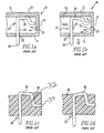
- the mold is shown generally at numeral 10 and has an upper die 12 and an opposed lower die 14.
- the mold also has an interior section 16 and an exterior section 18 with a connecting molding compound injection port 20.
- a conductive contact 24 is positioned in the contact and receiving aperture 22.
- the contact 24 has a vertical leg 26 with a contact terminal 28. It also has a horizontal leg 30 with an oblique section 32 and a terminal horizontal section 34.
- a molding compound is introduced to the interior 16 of the mold 10 through the injection port 20.
- the molding compound begins to fill the interior 16 of the mold 10 around the lead contact 24.
- the pressure of the molding compound may cause the contact to be flexed and displace it from its original position.
- the front of the horizontal leg 30 as the contact 24 is flexed downwardly and molded compound enters the space 36 between the contact 24 and the upper die 12.
- Fig. 1c the filling of the interior 16 of the mold 10 in the way shown in Fig.
- FIG. 1b may result in hardened molding compound 38 in position above the horizontal leg 30 in the completed connector.
- FIG. 1d it may also be possible that hardened molding compound 40 may be superimposed over the inner side of the horizontal leg 30 so that the leg extends obliquely upwardly as is shown in Fig. 1d. Consequently there may be an undesirable lack of coplanarity between the upper horizontal leg 30 of the contacts and the upper surface of the housing.
- JP-A-9286040 discloses a method for making a method for manufacturing an electrical connector comprising an insulative housing 40 with a base side 42 and an opposed side 44 and lateral sides 46, 48, 50, 52 interposed between said base side 42 and said opposed side 44 and at least one conductive contact 94 extending from the base side 42 of the insulation in a first leg and than laterially adjacent the top side of the housing 40 in a second leg 100, said method comprising the steps of:
- the present invention is a method for manufacturing an electrical connector comprising an insulative housing with a base side and an opposed side and lateral sides interposed between said base side and said opposed side and at least one conductive contact extending from the base side of the insulation in a first leg and then laterally adjacent the top side of the housing in a second leg.
- a mold comprising a first die and an opposed second die all defining an interior cavity and an exterior area.
- a molding compound input port extends between the exterior area and the interior cavity and a contact receiving aperture extending through the first die from the exterior area to the interior cavity.
- the conductive contact is then positioned so that the first leg extends upwardly from the exterior area through the contact receiving aperture into the interior cavity.
- the first leg extends through said interior cavity, and the second leg extends laterally adjacent the opposed die.
- the interior cavity of the mold is then filled with a polymeric molding compound, and force is applied on the second leg to cause the second leg of the contact to bear against the second die.
- a connector made according to the method of the present invention includes an insulative housing 40 which has a base side 42, a top side 44, a front lateral side 46 and a rear lateral side 48.
- This housing 40 also has opposed end lateral sides 50 and 52.
- On the top surface 44 there are opposed lateral raised areas 54 and 56 and a central recessed area 58.
- mounting apertures 60, 62 and 64 In the central recessed area 58 and extending vertically through the housing 40, mounting apertures 60, 62 and 64.
- a peripheral recess 66 Extending vertically through the housing and then positioned on the lateral raised areas 54 and 56 of the top surface 44, there are a plurality of contacts as at contact 68.
- This contact 68 includes, as does the other contacts, an upper solder tab 70 and a lower contact terminal 72.
- a mold is shown generally at numeral 74.
- This mold 74 includes a movable upper die 76 which includes a mold top surface 78.
- the mold 74 also includes stationery lower die 80 which includes a bottom surface 82 and lateral surfaces as at surface 84.
- the mold has an interior 86 which is connected to an exterior area 88 by means of a molding compound injection port 90.
- In the bottom surface 82 of the lower die 80 there is a contact receiving aperture 92.
- a contact shown generally at numeral 94 is engaged with the contact receiving aperture 92.
- This contact 94 has a vertical leg 96 with a terminal 98 that extends outwardly from the lower die 80.
- the vertical leg 96 also extends upwardly to adjacent the top surface 78 of the movable upper die 76. At this point the terminal extends laterally in a horizontal leg 100.
- An oblique section 102 extends in a forward and downward direction to horizontal mid-section 104.
- a force 108 acts on the upper edge 110 of the horizontal legs 100 of the contact 94.
- This force results in the contacts bending in the direction of arrow 112 which displaces the vertical leg to a position 96' shown in phantom in Figure 6.
- the oblique section also bends to position 114.
- this equal and opposite force 108 molding compound is prevented from being positioned between the top edge 110' of the horizontal leg 100' an the interior surface 78' of the upper die 76' of the mold. Consequently, the horizontal leg 100' of the contact 94, which may be a solder pad, will be coplanar or at least parallel with the upper surface 120 of the completed housing 122.
Landscapes
- Engineering & Computer Science (AREA)
- Manufacturing & Machinery (AREA)
- Manufacturing Of Electrical Connectors (AREA)
- Injection Moulding Of Plastics Or The Like (AREA)
- Connector Housings Or Holding Contact Members (AREA)
- Coupling Device And Connection With Printed Circuit (AREA)
Applications Claiming Priority (2)
| Application Number | Priority Date | Filing Date | Title |
|---|---|---|---|
| SG9904116A SG80641A1 (en) | 1999-08-30 | 1999-08-30 | Method for manufacturing electrical connectors for enhancing coplanarity |
| SG9904116 | 1999-08-30 |
Publications (3)
| Publication Number | Publication Date |
|---|---|
| EP1081811A2 EP1081811A2 (en) | 2001-03-07 |
| EP1081811A3 EP1081811A3 (en) | 2003-04-02 |
| EP1081811B1 true EP1081811B1 (en) | 2006-05-17 |
Family
ID=20430417
Family Applications (1)
| Application Number | Title | Priority Date | Filing Date |
|---|---|---|---|
| EP00118149A Expired - Lifetime EP1081811B1 (en) | 1999-08-30 | 2000-08-29 | Method for manufacturing electrical connectors for enhancing coplanarity |
Country Status (6)
| Country | Link |
|---|---|
| US (2) | US7000317B1 (enExample) |
| EP (1) | EP1081811B1 (enExample) |
| JP (1) | JP4540196B2 (enExample) |
| AT (1) | ATE326782T1 (enExample) |
| DE (1) | DE60027970T2 (enExample) |
| SG (1) | SG80641A1 (enExample) |
Families Citing this family (5)
| Publication number | Priority date | Publication date | Assignee | Title |
|---|---|---|---|---|
| JP4276526B2 (ja) * | 2003-11-26 | 2009-06-10 | 矢崎総業株式会社 | 電気接続箱や自動車の補機を制御する電子ユニットの構成部品とされるブスバー成形体及びその製造方法並びに電子ユニット |
| US7970699B1 (en) * | 2006-03-27 | 2011-06-28 | Loan Insights, Inc. | Customized consumer loan search and optimized loan pricing |
| DE102010046050A1 (de) | 2010-09-22 | 2012-03-22 | Tyco Electronics Amp Gmbh | Verfahren und Justagevorrichtung zum Ausrichten von Kontaktstiften eines elektrischen Bauteils sowie elektrisches Bauteil |
| TWM456013U (zh) * | 2012-07-27 | 2013-06-21 | Riidea Inc | 電源連接器端子之結構 |
| DE102013219861B4 (de) * | 2013-10-01 | 2016-05-12 | Fraunhofer-Gesellschaft zur Förderung der angewandten Forschung e.V. | Kontaktierungsverfahren |
Family Cites Families (17)
| Publication number | Priority date | Publication date | Assignee | Title |
|---|---|---|---|---|
| US4231628A (en) | 1978-12-14 | 1980-11-04 | Amp Incorporated | Electrical connector receptacles |
| JPS5882786U (ja) | 1981-11-30 | 1983-06-04 | ソニー株式会社 | マルチコネクタ |
| US4710134A (en) | 1986-09-29 | 1987-12-01 | Amp Incorporated | Low insertion force chip carrier connector with movable housing |
| US4817283A (en) * | 1987-08-21 | 1989-04-04 | Amp Incorporated | Method of forming a modular plug coupler |
| JPH06701Y2 (ja) * | 1989-07-19 | 1994-01-05 | 建設省関東地方建設局長 | 堤防を越える排水管 |
| US5167528A (en) * | 1990-04-20 | 1992-12-01 | Matsushita Electric Works, Ltd. | Method of manufacturing an electrical connector |
| JPH0416881U (enExample) * | 1990-05-31 | 1992-02-12 | ||
| JPH04181676A (ja) * | 1990-11-15 | 1992-06-29 | Hirose Electric Co Ltd | 電気コネクタとその製作方法 |
| JPH0562743A (ja) | 1991-08-30 | 1993-03-12 | Fujitsu Ltd | 電子装置におけるモジユール用コネクタ構造 |
| US5483843A (en) * | 1992-06-01 | 1996-01-16 | Thermo Separation Products Inc. | Transport apparatus |
| TW370305U (en) * | 1996-04-09 | 1999-09-11 | Hon Hai Prec Ind Co Ltd | Mold for cartridge connectors |
| JP3339300B2 (ja) | 1996-04-23 | 2002-10-28 | 矢崎総業株式会社 | コネクタの製造方法 |
| US5902136A (en) * | 1996-06-28 | 1999-05-11 | Berg Technology, Inc. | Electrical connector for use in miniaturized, high density, and high pin count applications and method of manufacture |
| JPH10217253A (ja) * | 1997-02-07 | 1998-08-18 | Sankyo Kasei Co Ltd | インサート成形法並びにインサート成形装置 |
| JP3239308B2 (ja) * | 1997-03-13 | 2001-12-17 | 矢崎総業株式会社 | インサート成形品の製造方法 |
| JPH11185926A (ja) * | 1997-12-25 | 1999-07-09 | Yazaki Corp | コネクタ、コネクタの製造方法及びこの製造方法に用いられる型構造 |
| JP3405201B2 (ja) * | 1998-06-17 | 2003-05-12 | 住友電装株式会社 | 機器用コネクタの製造方法 |
-
1999
- 1999-08-30 SG SG9904116A patent/SG80641A1/en unknown
-
2000
- 2000-08-29 AT AT00118149T patent/ATE326782T1/de not_active IP Right Cessation
- 2000-08-29 EP EP00118149A patent/EP1081811B1/en not_active Expired - Lifetime
- 2000-08-29 DE DE60027970T patent/DE60027970T2/de not_active Expired - Fee Related
- 2000-08-29 US US09/650,053 patent/US7000317B1/en not_active Expired - Fee Related
- 2000-08-30 JP JP2000260916A patent/JP4540196B2/ja not_active Expired - Fee Related
-
2005
- 2005-11-17 US US11/281,789 patent/US8056225B2/en not_active Expired - Fee Related
Also Published As
| Publication number | Publication date |
|---|---|
| SG80641A1 (en) | 2001-05-22 |
| EP1081811A2 (en) | 2001-03-07 |
| US8056225B2 (en) | 2011-11-15 |
| EP1081811A3 (en) | 2003-04-02 |
| JP4540196B2 (ja) | 2010-09-08 |
| US7000317B1 (en) | 2006-02-21 |
| DE60027970T2 (de) | 2007-04-26 |
| JP2001102147A (ja) | 2001-04-13 |
| DE60027970D1 (de) | 2006-06-22 |
| US20060075634A1 (en) | 2006-04-13 |
| ATE326782T1 (de) | 2006-06-15 |
Similar Documents
| Publication | Publication Date | Title |
|---|---|---|
| US6048482A (en) | Method for manufacturing an electrical connector | |
| US4231628A (en) | Electrical connector receptacles | |
| US4696525A (en) | Socket for stacking integrated circuit packages | |
| US4269467A (en) | Electrical connector receptacle having molded conductors | |
| US7270573B2 (en) | Electrical connector with load bearing features | |
| JP3078616B2 (ja) | プラグコネクタおよびその製造方法 | |
| JP2932152B2 (ja) | 電気コネクタに於ける端子及び電気コネクタの形成方法 | |
| JP3405201B2 (ja) | 機器用コネクタの製造方法 | |
| EP1081811B1 (en) | Method for manufacturing electrical connectors for enhancing coplanarity | |
| JP5382868B2 (ja) | 基板用同軸コネクタ、一対の連鎖端子、および基板用同軸コネクタを製造する製造方法 | |
| US6371816B1 (en) | Electric connector and a method of making same | |
| FI67458B (fi) | Elektriskt kontaktdon med stickkontakt och stickdosa och foerfarande foer dess framstaellning | |
| JP2942691B2 (ja) | コネクタ差込部付きインシュレータの製造方法 | |
| CN2515823Y (zh) | 电连接器 | |
| US6293826B1 (en) | Electrical connector with metal side members and method of producing same | |
| US7101793B2 (en) | Power module and its manufacturing method | |
| JPH04174989A (ja) | 雄端子の製造方法 | |
| EP0702434B1 (en) | Molded electrical connector | |
| JPH11149972A (ja) | 電気コネクタの製造方法 | |
| CN217507698U (zh) | 连接器固定件结构 | |
| JP2992425B2 (ja) | 回路基板 | |
| JP2786667B2 (ja) | 電気部品列の製造型 | |
| JP2684464B2 (ja) | フレキシブルコネクタの製造方法 | |
| JP2025012191A (ja) | コネクタの製造方法及びコネクタ | |
| US20040158982A1 (en) | Wire press-contact method and method of attaching press-contact terminal to connector housing |
Legal Events
| Date | Code | Title | Description |
|---|---|---|---|
| PUAI | Public reference made under article 153(3) epc to a published international application that has entered the european phase |
Free format text: ORIGINAL CODE: 0009012 |
|
| AK | Designated contracting states |
Kind code of ref document: A2 Designated state(s): AT BE CH CY DE DK ES FI FR GB GR IE IT LI LU MC NL PT SE |
|
| AX | Request for extension of the european patent |
Free format text: AL;LT;LV;MK;RO;SI |
|
| PUAL | Search report despatched |
Free format text: ORIGINAL CODE: 0009013 |
|
| AK | Designated contracting states |
Designated state(s): AT BE CH CY DE DK ES FI FR GB GR IE IT LI LU MC NL PT SE Kind code of ref document: A3 Designated state(s): AT BE CH CY DE DK ES FI FR GB GR IE IT LI LU MC NL PT SE |
|
| AX | Request for extension of the european patent |
Extension state: AL LT LV MK RO SI |
|
| 17P | Request for examination filed |
Effective date: 20030919 |
|
| AKX | Designation fees paid |
Designated state(s): AT BE CH CY DE DK ES FI FR GB GR IE IT LI LU MC NL PT SE |
|
| 17Q | First examination report despatched |
Effective date: 20031216 |
|
| GRAP | Despatch of communication of intention to grant a patent |
Free format text: ORIGINAL CODE: EPIDOSNIGR1 |
|
| GRAS | Grant fee paid |
Free format text: ORIGINAL CODE: EPIDOSNIGR3 |
|
| GRAA | (expected) grant |
Free format text: ORIGINAL CODE: 0009210 |
|
| RIN1 | Information on inventor provided before grant (corrected) |
Inventor name: SPYKERMAN,CONWAY FRANCIS |
|
| RAP1 | Party data changed (applicant data changed or rights of an application transferred) |
Owner name: FCI |
|
| AK | Designated contracting states |
Kind code of ref document: B1 Designated state(s): AT BE CH CY DE DK ES FI FR GB GR IE IT LI LU MC NL PT SE |
|
| PG25 | Lapsed in a contracting state [announced via postgrant information from national office to epo] |
Ref country code: IT Free format text: LAPSE BECAUSE OF FAILURE TO SUBMIT A TRANSLATION OF THE DESCRIPTION OR TO PAY THE FEE WITHIN THE PRESCRIBED TIME-LIMIT;WARNING: LAPSES OF ITALIAN PATENTS WITH EFFECTIVE DATE BEFORE 2007 MAY HAVE OCCURRED AT ANY TIME BEFORE 2007. THE CORRECT EFFECTIVE DATE MAY BE DIFFERENT FROM THE ONE RECORDED. Effective date: 20060517 Ref country code: FI Free format text: LAPSE BECAUSE OF FAILURE TO SUBMIT A TRANSLATION OF THE DESCRIPTION OR TO PAY THE FEE WITHIN THE PRESCRIBED TIME-LIMIT Effective date: 20060517 Ref country code: BE Free format text: LAPSE BECAUSE OF FAILURE TO SUBMIT A TRANSLATION OF THE DESCRIPTION OR TO PAY THE FEE WITHIN THE PRESCRIBED TIME-LIMIT Effective date: 20060517 Ref country code: NL Free format text: LAPSE BECAUSE OF FAILURE TO SUBMIT A TRANSLATION OF THE DESCRIPTION OR TO PAY THE FEE WITHIN THE PRESCRIBED TIME-LIMIT Effective date: 20060517 Ref country code: AT Free format text: LAPSE BECAUSE OF FAILURE TO SUBMIT A TRANSLATION OF THE DESCRIPTION OR TO PAY THE FEE WITHIN THE PRESCRIBED TIME-LIMIT Effective date: 20060517 Ref country code: CH Free format text: LAPSE BECAUSE OF FAILURE TO SUBMIT A TRANSLATION OF THE DESCRIPTION OR TO PAY THE FEE WITHIN THE PRESCRIBED TIME-LIMIT Effective date: 20060517 Ref country code: LI Free format text: LAPSE BECAUSE OF FAILURE TO SUBMIT A TRANSLATION OF THE DESCRIPTION OR TO PAY THE FEE WITHIN THE PRESCRIBED TIME-LIMIT Effective date: 20060517 |
|
| REG | Reference to a national code |
Ref country code: GB Ref legal event code: FG4D |
|
| REG | Reference to a national code |
Ref country code: CH Ref legal event code: EP |
|
| REG | Reference to a national code |
Ref country code: IE Ref legal event code: FG4D |
|
| REF | Corresponds to: |
Ref document number: 60027970 Country of ref document: DE Date of ref document: 20060622 Kind code of ref document: P |
|
| PG25 | Lapsed in a contracting state [announced via postgrant information from national office to epo] |
Ref country code: SE Free format text: LAPSE BECAUSE OF FAILURE TO SUBMIT A TRANSLATION OF THE DESCRIPTION OR TO PAY THE FEE WITHIN THE PRESCRIBED TIME-LIMIT Effective date: 20060817 Ref country code: DK Free format text: LAPSE BECAUSE OF FAILURE TO SUBMIT A TRANSLATION OF THE DESCRIPTION OR TO PAY THE FEE WITHIN THE PRESCRIBED TIME-LIMIT Effective date: 20060817 |
|
| PG25 | Lapsed in a contracting state [announced via postgrant information from national office to epo] |
Ref country code: ES Free format text: LAPSE BECAUSE OF FAILURE TO SUBMIT A TRANSLATION OF THE DESCRIPTION OR TO PAY THE FEE WITHIN THE PRESCRIBED TIME-LIMIT Effective date: 20060828 |
|
| PG25 | Lapsed in a contracting state [announced via postgrant information from national office to epo] |
Ref country code: IE Free format text: LAPSE BECAUSE OF NON-PAYMENT OF DUE FEES Effective date: 20060829 |
|
| PG25 | Lapsed in a contracting state [announced via postgrant information from national office to epo] |
Ref country code: MC Free format text: LAPSE BECAUSE OF NON-PAYMENT OF DUE FEES Effective date: 20060831 |
|
| PG25 | Lapsed in a contracting state [announced via postgrant information from national office to epo] |
Ref country code: PT Free format text: LAPSE BECAUSE OF FAILURE TO SUBMIT A TRANSLATION OF THE DESCRIPTION OR TO PAY THE FEE WITHIN THE PRESCRIBED TIME-LIMIT Effective date: 20061017 |
|
| NLV1 | Nl: lapsed or annulled due to failure to fulfill the requirements of art. 29p and 29m of the patents act | ||
| ET | Fr: translation filed | ||
| REG | Reference to a national code |
Ref country code: CH Ref legal event code: PL |
|
| PLBE | No opposition filed within time limit |
Free format text: ORIGINAL CODE: 0009261 |
|
| STAA | Information on the status of an ep patent application or granted ep patent |
Free format text: STATUS: NO OPPOSITION FILED WITHIN TIME LIMIT |
|
| 26N | No opposition filed |
Effective date: 20070220 |
|
| PGFP | Annual fee paid to national office [announced via postgrant information from national office to epo] |
Ref country code: DE Payment date: 20070831 Year of fee payment: 8 |
|
| PGFP | Annual fee paid to national office [announced via postgrant information from national office to epo] |
Ref country code: GB Payment date: 20070705 Year of fee payment: 8 |
|
| PG25 | Lapsed in a contracting state [announced via postgrant information from national office to epo] |
Ref country code: GR Free format text: LAPSE BECAUSE OF FAILURE TO SUBMIT A TRANSLATION OF THE DESCRIPTION OR TO PAY THE FEE WITHIN THE PRESCRIBED TIME-LIMIT Effective date: 20060818 |
|
| PGFP | Annual fee paid to national office [announced via postgrant information from national office to epo] |
Ref country code: FR Payment date: 20070803 Year of fee payment: 8 |
|
| PG25 | Lapsed in a contracting state [announced via postgrant information from national office to epo] |
Ref country code: LU Free format text: LAPSE BECAUSE OF NON-PAYMENT OF DUE FEES Effective date: 20060829 |
|
| PG25 | Lapsed in a contracting state [announced via postgrant information from national office to epo] |
Ref country code: CY Free format text: LAPSE BECAUSE OF FAILURE TO SUBMIT A TRANSLATION OF THE DESCRIPTION OR TO PAY THE FEE WITHIN THE PRESCRIBED TIME-LIMIT Effective date: 20060517 |
|
| GBPC | Gb: european patent ceased through non-payment of renewal fee |
Effective date: 20080829 |
|
| REG | Reference to a national code |
Ref country code: FR Ref legal event code: ST Effective date: 20090430 |
|
| PG25 | Lapsed in a contracting state [announced via postgrant information from national office to epo] |
Ref country code: FR Free format text: LAPSE BECAUSE OF NON-PAYMENT OF DUE FEES Effective date: 20080901 Ref country code: DE Free format text: LAPSE BECAUSE OF NON-PAYMENT OF DUE FEES Effective date: 20090303 |
|
| PG25 | Lapsed in a contracting state [announced via postgrant information from national office to epo] |
Ref country code: GB Free format text: LAPSE BECAUSE OF NON-PAYMENT OF DUE FEES Effective date: 20080829 |