EP1078352B1 - A bus arrangement for a driver of a matrix display - Google Patents
A bus arrangement for a driver of a matrix display Download PDFInfo
- Publication number
- EP1078352B1 EP1078352B1 EP99921838.1A EP99921838A EP1078352B1 EP 1078352 B1 EP1078352 B1 EP 1078352B1 EP 99921838 A EP99921838 A EP 99921838A EP 1078352 B1 EP1078352 B1 EP 1078352B1
- Authority
- EP
- European Patent Office
- Prior art keywords
- semiconductor switches
- conductors
- terminal
- terminals
- data
- Prior art date
- Legal status (The legal status is an assumption and is not a legal conclusion. Google has not performed a legal analysis and makes no representation as to the accuracy of the status listed.)
- Expired - Lifetime
Links
- 239000011159 matrix material Substances 0.000 title description 6
- 239000004020 conductor Substances 0.000 claims description 45
- 239000003990 capacitor Substances 0.000 claims description 7
- 230000008878 coupling Effects 0.000 claims description 3
- 238000010168 coupling process Methods 0.000 claims description 3
- 238000005859 coupling reaction Methods 0.000 claims description 3
- 239000004065 semiconductor Substances 0.000 claims 12
- 239000004973 liquid crystal related substance Substances 0.000 description 10
- 239000002184 metal Substances 0.000 description 4
- 238000003491 array Methods 0.000 description 3
- 210000002858 crystal cell Anatomy 0.000 description 3
- 238000005070 sampling Methods 0.000 description 3
- 238000000034 method Methods 0.000 description 2
- 239000010409 thin film Substances 0.000 description 2
- 230000006870 function Effects 0.000 description 1
Images
Classifications
-
- G—PHYSICS
- G09—EDUCATION; CRYPTOGRAPHY; DISPLAY; ADVERTISING; SEALS
- G09G—ARRANGEMENTS OR CIRCUITS FOR CONTROL OF INDICATING DEVICES USING STATIC MEANS TO PRESENT VARIABLE INFORMATION
- G09G5/00—Control arrangements or circuits for visual indicators common to cathode-ray tube indicators and other visual indicators
- G09G5/10—Intensity circuits
-
- G—PHYSICS
- G09—EDUCATION; CRYPTOGRAPHY; DISPLAY; ADVERTISING; SEALS
- G09G—ARRANGEMENTS OR CIRCUITS FOR CONTROL OF INDICATING DEVICES USING STATIC MEANS TO PRESENT VARIABLE INFORMATION
- G09G3/00—Control arrangements or circuits, of interest only in connection with visual indicators other than cathode-ray tubes
- G09G3/20—Control arrangements or circuits, of interest only in connection with visual indicators other than cathode-ray tubes for presentation of an assembly of a number of characters, e.g. a page, by composing the assembly by combination of individual elements arranged in a matrix no fixed position being assigned to or needed to be assigned to the individual characters or partial characters
- G09G3/34—Control arrangements or circuits, of interest only in connection with visual indicators other than cathode-ray tubes for presentation of an assembly of a number of characters, e.g. a page, by composing the assembly by combination of individual elements arranged in a matrix no fixed position being assigned to or needed to be assigned to the individual characters or partial characters by control of light from an independent source
- G09G3/36—Control arrangements or circuits, of interest only in connection with visual indicators other than cathode-ray tubes for presentation of an assembly of a number of characters, e.g. a page, by composing the assembly by combination of individual elements arranged in a matrix no fixed position being assigned to or needed to be assigned to the individual characters or partial characters by control of light from an independent source using liquid crystals
- G09G3/3611—Control of matrices with row and column drivers
- G09G3/3685—Details of drivers for data electrodes
- G09G3/3688—Details of drivers for data electrodes suitable for active matrices only
-
- G—PHYSICS
- G09—EDUCATION; CRYPTOGRAPHY; DISPLAY; ADVERTISING; SEALS
- G09G—ARRANGEMENTS OR CIRCUITS FOR CONTROL OF INDICATING DEVICES USING STATIC MEANS TO PRESENT VARIABLE INFORMATION
- G09G2310/00—Command of the display device
- G09G2310/02—Addressing, scanning or driving the display screen or processing steps related thereto
- G09G2310/0264—Details of driving circuits
- G09G2310/027—Details of drivers for data electrodes, the drivers handling digital grey scale data, e.g. use of D/A converters
-
- G—PHYSICS
- G09—EDUCATION; CRYPTOGRAPHY; DISPLAY; ADVERTISING; SEALS
- G09G—ARRANGEMENTS OR CIRCUITS FOR CONTROL OF INDICATING DEVICES USING STATIC MEANS TO PRESENT VARIABLE INFORMATION
- G09G2310/00—Command of the display device
- G09G2310/02—Addressing, scanning or driving the display screen or processing steps related thereto
- G09G2310/0264—Details of driving circuits
- G09G2310/0297—Special arrangements with multiplexing or demultiplexing of display data in the drivers for data electrodes, in a pre-processing circuitry delivering display data to said drivers or in the matrix panel, e.g. multiplexing plural data signals to one D/A converter or demultiplexing the D/A converter output to multiple columns
-
- G—PHYSICS
- G09—EDUCATION; CRYPTOGRAPHY; DISPLAY; ADVERTISING; SEALS
- G09G—ARRANGEMENTS OR CIRCUITS FOR CONTROL OF INDICATING DEVICES USING STATIC MEANS TO PRESENT VARIABLE INFORMATION
- G09G3/00—Control arrangements or circuits, of interest only in connection with visual indicators other than cathode-ray tubes
- G09G3/20—Control arrangements or circuits, of interest only in connection with visual indicators other than cathode-ray tubes for presentation of an assembly of a number of characters, e.g. a page, by composing the assembly by combination of individual elements arranged in a matrix no fixed position being assigned to or needed to be assigned to the individual characters or partial characters
- G09G3/22—Control arrangements or circuits, of interest only in connection with visual indicators other than cathode-ray tubes for presentation of an assembly of a number of characters, e.g. a page, by composing the assembly by combination of individual elements arranged in a matrix no fixed position being assigned to or needed to be assigned to the individual characters or partial characters using controlled light sources
- G09G3/28—Control arrangements or circuits, of interest only in connection with visual indicators other than cathode-ray tubes for presentation of an assembly of a number of characters, e.g. a page, by composing the assembly by combination of individual elements arranged in a matrix no fixed position being assigned to or needed to be assigned to the individual characters or partial characters using controlled light sources using luminous gas-discharge panels, e.g. plasma panels
-
- G—PHYSICS
- G09—EDUCATION; CRYPTOGRAPHY; DISPLAY; ADVERTISING; SEALS
- G09G—ARRANGEMENTS OR CIRCUITS FOR CONTROL OF INDICATING DEVICES USING STATIC MEANS TO PRESENT VARIABLE INFORMATION
- G09G3/00—Control arrangements or circuits, of interest only in connection with visual indicators other than cathode-ray tubes
- G09G3/20—Control arrangements or circuits, of interest only in connection with visual indicators other than cathode-ray tubes for presentation of an assembly of a number of characters, e.g. a page, by composing the assembly by combination of individual elements arranged in a matrix no fixed position being assigned to or needed to be assigned to the individual characters or partial characters
- G09G3/34—Control arrangements or circuits, of interest only in connection with visual indicators other than cathode-ray tubes for presentation of an assembly of a number of characters, e.g. a page, by composing the assembly by combination of individual elements arranged in a matrix no fixed position being assigned to or needed to be assigned to the individual characters or partial characters by control of light from an independent source
- G09G3/36—Control arrangements or circuits, of interest only in connection with visual indicators other than cathode-ray tubes for presentation of an assembly of a number of characters, e.g. a page, by composing the assembly by combination of individual elements arranged in a matrix no fixed position being assigned to or needed to be assigned to the individual characters or partial characters by control of light from an independent source using liquid crystals
- G09G3/3611—Control of matrices with row and column drivers
- G09G3/3685—Details of drivers for data electrodes
Definitions
- This invention relates generally to a bus arrangement for display devices and particularly to a system for applying brightness signals to pixels of a display device, such as a liquid crystal display (LCD) or a plasma display.
- a display device such as a liquid crystal display (LCD) or a plasma display.
- Display devices such as liquid crystal displays or plasma displays, are composed of a matrix or an array of pixels arranged horizontally in rows and vertically in columns.
- the video information to be displayed is applied as brightness (gray scale) signals to data lines which are individually associated with each column of pixels.
- the rows of pixels are sequentially scanned and the capacitances of the pixels within the activated row are charged to the various brightness levels in accordance with the levels of the brightness signals applied to the individual columns.
- the M brightness information signals are applied to an input port of an input demultiplexer of the array.
- the demultiplexer converts the M brightness information signals to MXN signals developed in MXN parallel conductors that are coupled via MXN data line drives to MXN column conductors of the array.
- the input demultiplexer may be formed by MXN thin film transistor (TFT's). Groups of M parallel conductors are successively selected, during each horizontal line interval of the video signal. The selection of each group of M parallel conductors is obtained by selection pulse signals developed in a bus of N parallel conductors.
- the capacitance of the input busing structure associated with the N selection parallel conductors and the input busing structure associated with the M brightness information carrying parallel conductors can be a major source of both power dissipation and yield loss, especially for higher resolution self-scanned Active Matrix Liquid Crystal Displays (AMLCDs).
- AMLCDs Active Matrix Liquid Crystal Displays
- Long metal runs across the display and multiple crossovers (Source/Drain metal-to-Gate metal) cause significant capacitive loads, resulting in both capacitance shorting failures, unwanted crosstalk among the brightness information carrying conductors and excessive dynamic power dissipation. It is desirable to reduce the number of crossovers of the input busing structure associated with the N selection parallel conductors and of the input busing structure associated with the M brightness information carrying parallel conductors.
- Dependant claim relates to an advantageous embodiment.
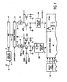
- FIGURE 1 illustrates an integrated driver arrangement for storing information in an SVGA liquid crystal array. It should be understood that the invention may be utilized for storing information in pixels of a plasma display.
- Analog circuitry 11 receives a video signal representative of picture information to be displayed from, for example, an antenna 12. The analog circuitry 11 provides a video signal on a line 13 as an input signal to an analog-to-digital converter (A/D) 14.
- A/D analog-to-digital converter
- A/D converter 14 includes an output bus 19-to provide brightness levels, or gray scale codes, to a memory 21 having 100 groups of output lines 22. Each group of output lines 22 of memory 21 applies the stored digital information to a corresponding digital-to-analog (D/A) converter 23. There are 100 D/A converters 23 that correspond to the 100 groups of lines 22, respectively.
- An output analog signal DBS(j) from a given D/A converter 23 is coupled via a corresponding brightness information carrying conductor DB(j) to a demultiplexer transistor MN1 associated with a corresponding column.
- Transistors MN1 may be thin film transistors (TFTs).
- TFTs thin film transistors
- Demultiplexer transistor MN1 applies the information of signal DBS(j) carried on corresponding brightness information carrying conductor DB(j) to a corresponding sampling capacitor C43 for storing an analog signal VC43 in capacitor C43.
- Signal VC43 is coupled to a corresponding data line driver 100 that drives corresponding data line 17 associated with a corresponding column.
- a select line scanner 60 produces row select signals in lines 18 for selecting, in a conventional manner, a given row of array 16.
- the voltages carried in 100 data lines 17 are applied during a 32 microsecond line time to pixels 16a of the selected row.
- the sampling in a given group of 100 signals DBS(j) of FIGURE 1 carried in brightness information carrying conductors DB(j) occurs simultaneously under the control of a corresponding data-word pulse signal DWS(i) forming a selection word.
- the symbol (i) assumes values from 1 to 24 associated with the 24 separate conductors DW(i).
- Each pulse signal DWS(i) controls the sampling of a corresponding group of 100 signals DBS(j) in capacitors C43.
- a two-stage pipeline cycle may be used.
- Signals DBS(j) are demultiplexed and stored in 2400 capacitors C43 by the operation of pulse signals DWS(i). Then, the information in capacitors C43 is transferred simultaneously to data line driver 100. Thus, capacitors C43 become available for the demultiplexing of the next row information, while the previous row information is applied to the pixels.
- FIGURE 1 may operate, for example, similarly to that described in, for example, U. S. Patent No. 5,673,063 in the name of Sherman Weisbrod , entitled "A DATA LINE DRIVER FOR APPLYING BRIGHTNESS SIGNALS TO A DISPLAY".
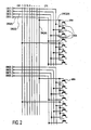
- the busing arrangement of conductors DW(i) and DB(j), embodying an inventive feature, is explained in connection with FIGURE 2 . Similar symbols and numerals in FIGURES 1 and 2 indicate similar items or functions.
- the crossover capacitance of the input busing structure associated with conductors DW(i) and DB(j) can be a major source of both power dissipation and yield loss, especially for higher resolution self-scanned Active Matrix Liquid Crystal Displays (AMLCDs).
- AMLCDs Active Matrix Liquid Crystal Displays
- Long metal runs across the display and multiple crossovers (Source/Drain metal-to-Gate metal) cause significant capacitive loads, resulting in both capacitance shorting failures, unwanted crosstalk among the brightness information carrying conductors, and excessive dynamic power dissipation.
- the busing arrangement of FIGURE 2 reduces the number of capacitive crossovers associated with the input bus structure thus reducing the power dissipation and improving yield.
- the brightness information carrying conductors DB(j) instead of being arranged individually and uniformly across the display, are grouped together into local “clusters” such as, for example, brightness information carrying conductors DB(1) - DB(4).
- the cluster of brightness information carrying conductors DB(1) - DB(4) are coupled to four transistors MN1 having gate electrodes that share, in common, conductor DW(24).
- the number of crossovers of brightness information carrying conductors DB(j)-to-data-word conductors DW(i) have been reduced by a factor of about 4 : 1. This, advantageously, reduces dynamic power dissipation, improves yield and reduces the crosstalk among the brightness information carrying-conductors.
- the cluster busing arrangement adds a multiplicity of new local sub-arrays DBSA to the bus structure. Although these new local sub-arrays do add some additional crossovers of their own (2.5 per brightness information carrying conductor), this is a small price to pay for reducing the average number of crossovers in the main brightness information carrying conductor to data-word conductor matrix from 20/data-line to only 5/data-line. The total capacitive coupling in the input bus structure is thereby cut by a factor of approximately 4 using the cluster bus technique.
- cluster busing therefore, include higher yield, lower power dissipation, and reduced crosstalk.
- another advantage to cluster busing is that we now break up the pattern of consecutive columns connected to a single signal DBS(j). Small errors in signal DBS(j)-to-signal DBS(j) will normally result in noticeable "block” errors because the human eye is very sensitive to large block patterns. Using the cluster bus technique, the blocks are broken-up into a finer pitch that is, advantageously, less obvious to the viewer.
- the structure may be improved through the addition of clusters of sub-arrays to reduce the complexity and capacitance of the main array.
Landscapes
- Engineering & Computer Science (AREA)
- Physics & Mathematics (AREA)
- Computer Hardware Design (AREA)
- General Physics & Mathematics (AREA)
- Theoretical Computer Science (AREA)
- Chemical & Material Sciences (AREA)
- Crystallography & Structural Chemistry (AREA)
- Control Of Indicators Other Than Cathode Ray Tubes (AREA)
- Liquid Crystal Display Device Control (AREA)
- Liquid Crystal (AREA)
- Electronic Switches (AREA)
Applications Claiming Priority (3)
| Application Number | Priority Date | Filing Date | Title |
|---|---|---|---|
| US8576698P | 1998-05-16 | 1998-05-16 | |
| PCT/US1999/010227 WO1999060555A2 (en) | 1998-05-16 | 1999-05-11 | A buss arrangement for a driver of a matrix display |
| US85766P | 2008-08-01 |
Publications (2)
| Publication Number | Publication Date |
|---|---|
| EP1078352A2 EP1078352A2 (en) | 2001-02-28 |
| EP1078352B1 true EP1078352B1 (en) | 2015-07-08 |
Family
ID=22193802
Family Applications (1)
| Application Number | Title | Priority Date | Filing Date |
|---|---|---|---|
| EP99921838.1A Expired - Lifetime EP1078352B1 (en) | 1998-05-16 | 1999-05-11 | A bus arrangement for a driver of a matrix display |
Country Status (9)
| Country | Link |
|---|---|
| EP (1) | EP1078352B1 (enExample) |
| JP (1) | JP5240884B2 (enExample) |
| KR (1) | KR100660446B1 (enExample) |
| CN (1) | CN1183501C (enExample) |
| AU (1) | AU3894799A (enExample) |
| MX (1) | MXPA00011202A (enExample) |
| TW (1) | TW519612B (enExample) |
| WO (1) | WO1999060555A2 (enExample) |
| ZA (1) | ZA200006423B (enExample) |
Families Citing this family (15)
| Publication number | Priority date | Publication date | Assignee | Title |
|---|---|---|---|---|
| KR100578911B1 (ko) | 2003-11-26 | 2006-05-11 | 삼성에스디아이 주식회사 | 전류 역다중화 장치 및 이를 이용한 전류 기입형 표시 장치 |
| KR100578913B1 (ko) | 2003-11-27 | 2006-05-11 | 삼성에스디아이 주식회사 | 역다중화기를 이용한 표시 장치 및 그 구동 방법 |
| KR100578914B1 (ko) | 2003-11-27 | 2006-05-11 | 삼성에스디아이 주식회사 | 역다중화기를 이용한 표시 장치 |
| KR100589381B1 (ko) | 2003-11-27 | 2006-06-14 | 삼성에스디아이 주식회사 | 역다중화기를 이용한 표시 장치 및 그 구동 방법 |
| KR101126343B1 (ko) | 2004-04-30 | 2012-03-23 | 엘지디스플레이 주식회사 | 일렉트로-루미네센스 표시장치 |
| KR100600350B1 (ko) * | 2004-05-15 | 2006-07-14 | 삼성에스디아이 주식회사 | 역다중화 및 이를 구비한 유기 전계발광 표시 장치 |
| KR100622217B1 (ko) | 2004-05-25 | 2006-09-08 | 삼성에스디아이 주식회사 | 유기 전계발광 표시장치 및 역다중화부 |
| TWI309813B (en) | 2005-12-23 | 2009-05-11 | Au Optronics Corp | Display device and pixel testing method thereof |
| JP6064313B2 (ja) | 2011-10-18 | 2017-01-25 | セイコーエプソン株式会社 | 電気光学装置、電気光学装置の駆動方法および電子機器 |
| JP6141590B2 (ja) | 2011-10-18 | 2017-06-07 | セイコーエプソン株式会社 | 電気光学装置および電子機器 |
| JP2014029438A (ja) * | 2012-07-31 | 2014-02-13 | Sony Corp | 表示装置、駆動回路、および電子機器 |
| JP6535441B2 (ja) * | 2014-08-06 | 2019-06-26 | セイコーエプソン株式会社 | 電気光学装置、電子機器、及び電気光学装置の駆動方法 |
| JP6626802B2 (ja) * | 2016-09-07 | 2019-12-25 | セイコーエプソン株式会社 | 電気光学装置および電子機器 |
| JP6581951B2 (ja) * | 2016-09-07 | 2019-09-25 | セイコーエプソン株式会社 | 電気光学装置の駆動方法 |
| JP6702352B2 (ja) * | 2018-05-07 | 2020-06-03 | セイコーエプソン株式会社 | 電気光学装置及び電子機器 |
Citations (1)
| Publication number | Priority date | Publication date | Assignee | Title |
|---|---|---|---|---|
| JPH03121415A (ja) * | 1989-06-30 | 1991-05-23 | Toshiba Corp | ディスプレイ装置 |
Family Cites Families (5)
| Publication number | Priority date | Publication date | Assignee | Title |
|---|---|---|---|---|
| EP0238867B1 (en) * | 1986-02-21 | 1994-12-14 | Canon Kabushiki Kaisha | Display apparatus |
| US5170158A (en) * | 1989-06-30 | 1992-12-08 | Kabushiki Kaisha Toshiba | Display apparatus |
| JPH07152350A (ja) * | 1993-11-30 | 1995-06-16 | Sharp Corp | 表示装置及びその駆動方法 |
| JP3403027B2 (ja) * | 1996-10-18 | 2003-05-06 | キヤノン株式会社 | 映像水平回路 |
| JP4011715B2 (ja) * | 1997-03-03 | 2007-11-21 | 東芝松下ディスプレイテクノロジー株式会社 | 表示装置 |
-
1999
- 1999-05-11 EP EP99921838.1A patent/EP1078352B1/en not_active Expired - Lifetime
- 1999-05-11 WO PCT/US1999/010227 patent/WO1999060555A2/en not_active Ceased
- 1999-05-11 MX MXPA00011202A patent/MXPA00011202A/es active IP Right Grant
- 1999-05-11 CN CNB998062235A patent/CN1183501C/zh not_active Expired - Lifetime
- 1999-05-11 JP JP2000550091A patent/JP5240884B2/ja not_active Expired - Lifetime
- 1999-05-11 AU AU38947/99A patent/AU3894799A/en not_active Abandoned
- 1999-05-11 KR KR1020007012843A patent/KR100660446B1/ko not_active Expired - Lifetime
- 1999-05-15 TW TW088107917A patent/TW519612B/zh not_active IP Right Cessation
-
2000
- 2000-11-08 ZA ZA200006423A patent/ZA200006423B/xx unknown
Patent Citations (1)
| Publication number | Priority date | Publication date | Assignee | Title |
|---|---|---|---|---|
| JPH03121415A (ja) * | 1989-06-30 | 1991-05-23 | Toshiba Corp | ディスプレイ装置 |
Also Published As
| Publication number | Publication date |
|---|---|
| EP1078352A2 (en) | 2001-02-28 |
| TW519612B (en) | 2003-02-01 |
| AU3894799A (en) | 1999-12-06 |
| KR20010043655A (ko) | 2001-05-25 |
| WO1999060555A3 (en) | 2000-03-09 |
| JP2002516417A (ja) | 2002-06-04 |
| JP5240884B2 (ja) | 2013-07-17 |
| KR100660446B1 (ko) | 2006-12-22 |
| CN1301377A (zh) | 2001-06-27 |
| WO1999060555A2 (en) | 1999-11-25 |
| MXPA00011202A (es) | 2003-04-22 |
| CN1183501C (zh) | 2005-01-05 |
| ZA200006423B (en) | 2002-01-30 |
Similar Documents
| Publication | Publication Date | Title |
|---|---|---|
| EP1078352B1 (en) | A bus arrangement for a driver of a matrix display | |
| KR100323913B1 (ko) | 반도체장치 | |
| JPH06148680A (ja) | マトリクス型液晶表示装置 | |
| JPS59111197A (ja) | マトリクス型表示装置の駆動回路 | |
| GR3024364T3 (en) | Data driving circuit for lcd display. | |
| WO2003042964A2 (en) | Liquid crystal display | |
| DE69406267D1 (de) | Datentreibervorrichtung für verwendung in einer flüssigkristallanzeige | |
| US20060146211A1 (en) | Non rectangular display device | |
| CN110136630A (zh) | 一种显示面板及其驱动方法、显示装置 | |
| KR100262226B1 (ko) | 평면패널 표시장치 및 그 구동방법 | |
| US11587485B2 (en) | Display panel, method for driving the same, and display device | |
| US10991327B2 (en) | Method of driving pixel arrangement structure and display panel and display apparatus associated therewith | |
| US12067925B2 (en) | Display panel and electronic terminal | |
| US12236838B2 (en) | Display panel, driving method thereof, and display device | |
| US6825836B1 (en) | Bus arrangement for a driver of a matrix display | |
| US6703996B2 (en) | Device and method for addressing LCD pixels | |
| US6636196B2 (en) | Electro-optic display device using a multi-row addressing scheme | |
| CN220731152U (zh) | 电子纸显示装置、显示面板和显示装置 | |
| US12118162B1 (en) | Touch display drive circuit, drive method and touch display panel | |
| US20070139403A1 (en) | Visual Display Driver and Method of Operating Same | |
| KR100528351B1 (ko) | 액정표시장치의 구동방법 및 패널구조 | |
| JPH11174486A (ja) | 液晶表示装置 | |
| KR20010004898A (ko) | 액정 디스플레이의 구동방법 | |
| JPH05313604A (ja) | 表示装置 |
Legal Events
| Date | Code | Title | Description |
|---|---|---|---|
| PUAI | Public reference made under article 153(3) epc to a published international application that has entered the european phase |
Free format text: ORIGINAL CODE: 0009012 |
|
| 17P | Request for examination filed |
Effective date: 20001102 |
|
| AK | Designated contracting states |
Kind code of ref document: A2 Designated state(s): DE FR GB |
|
| 17Q | First examination report despatched |
Effective date: 20011015 |
|
| RBV | Designated contracting states (corrected) |
Designated state(s): DE FR GB |
|
| RAP1 | Party data changed (applicant data changed or rights of an application transferred) |
Owner name: THOMSON LICENSING |
|
| RAP1 | Party data changed (applicant data changed or rights of an application transferred) |
Owner name: THOMSON LICENSING |
|
| REG | Reference to a national code |
Ref country code: DE Ref legal event code: R079 Ref document number: 69945360 Country of ref document: DE Free format text: PREVIOUS MAIN CLASS: G09G0001000000 Ipc: G09G0003360000 |
|
| GRAP | Despatch of communication of intention to grant a patent |
Free format text: ORIGINAL CODE: EPIDOSNIGR1 |
|
| RIC1 | Information provided on ipc code assigned before grant |
Ipc: G09G 3/36 20060101AFI20150119BHEP Ipc: G09G 3/28 20130101ALI20150119BHEP |
|
| INTG | Intention to grant announced |
Effective date: 20150211 |
|
| GRAS | Grant fee paid |
Free format text: ORIGINAL CODE: EPIDOSNIGR3 |
|
| GRAA | (expected) grant |
Free format text: ORIGINAL CODE: 0009210 |
|
| AK | Designated contracting states |
Kind code of ref document: B1 Designated state(s): DE FR GB |
|
| REG | Reference to a national code |
Ref country code: GB Ref legal event code: FG4D |
|
| REG | Reference to a national code |
Ref country code: DE Ref legal event code: R084 Ref document number: 69945360 Country of ref document: DE |
|
| REG | Reference to a national code |
Ref country code: DE Ref legal event code: R096 Ref document number: 69945360 Country of ref document: DE |
|
| REG | Reference to a national code |
Ref country code: DE Ref legal event code: R097 Ref document number: 69945360 Country of ref document: DE |
|
| PLBE | No opposition filed within time limit |
Free format text: ORIGINAL CODE: 0009261 |
|
| STAA | Information on the status of an ep patent application or granted ep patent |
Free format text: STATUS: NO OPPOSITION FILED WITHIN TIME LIMIT |
|
| REG | Reference to a national code |
Ref country code: FR Ref legal event code: PLFP Year of fee payment: 18 |
|
| 26N | No opposition filed |
Effective date: 20160411 |
|
| GBPC | Gb: european patent ceased through non-payment of renewal fee |
Effective date: 20160511 |
|
| REG | Reference to a national code |
Ref country code: FR Ref legal event code: PLFP Year of fee payment: 19 |
|
| PG25 | Lapsed in a contracting state [announced via postgrant information from national office to epo] |
Ref country code: GB Free format text: LAPSE BECAUSE OF NON-PAYMENT OF DUE FEES Effective date: 20160511 |
|
| REG | Reference to a national code |
Ref country code: DE Ref legal event code: R082 Ref document number: 69945360 Country of ref document: DE Representative=s name: DEHNS, DE Ref country code: DE Ref legal event code: R082 Ref document number: 69945360 Country of ref document: DE Representative=s name: HOFSTETTER, SCHURACK & PARTNER PATENT- UND REC, DE |
|
| REG | Reference to a national code |
Ref country code: FR Ref legal event code: PLFP Year of fee payment: 20 |
|
| PGFP | Annual fee paid to national office [announced via postgrant information from national office to epo] |
Ref country code: DE Payment date: 20180517 Year of fee payment: 20 |
|
| PGFP | Annual fee paid to national office [announced via postgrant information from national office to epo] |
Ref country code: FR Payment date: 20180523 Year of fee payment: 20 |
|
| REG | Reference to a national code |
Ref country code: FR Ref legal event code: TP Owner name: THOMSON LICENSING DTV, FR Effective date: 20180830 |
|
| REG | Reference to a national code |
Ref country code: DE Ref legal event code: R082 Ref document number: 69945360 Country of ref document: DE Representative=s name: DEHNS, DE Ref country code: DE Ref legal event code: R081 Ref document number: 69945360 Country of ref document: DE Owner name: INTERDIGITAL MADISON PATENT HOLDINGS, FR Free format text: FORMER OWNER: THOMSON LICENSING, ISSY-LES-MOULINEAUX, FR |
|
| REG | Reference to a national code |
Ref country code: DE Ref legal event code: R071 Ref document number: 69945360 Country of ref document: DE |