EP1069650B1 - Metallkontakt - Google Patents
Metallkontakt Download PDFInfo
- Publication number
- EP1069650B1 EP1069650B1 EP00305643A EP00305643A EP1069650B1 EP 1069650 B1 EP1069650 B1 EP 1069650B1 EP 00305643 A EP00305643 A EP 00305643A EP 00305643 A EP00305643 A EP 00305643A EP 1069650 B1 EP1069650 B1 EP 1069650B1
- Authority
- EP
- European Patent Office
- Prior art keywords
- metal terminal
- contact
- installing hole
- terminal
- contact hole
- Prior art date
- Legal status (The legal status is an assumption and is not a legal conclusion. Google has not performed a legal analysis and makes no representation as to the accuracy of the status listed.)
- Expired - Lifetime
Links
Images

Classifications
-
- H—ELECTRICITY
- H01—ELECTRIC ELEMENTS
- H01R—ELECTRICALLY-CONDUCTIVE CONNECTIONS; STRUCTURAL ASSOCIATIONS OF A PLURALITY OF MUTUALLY-INSULATED ELECTRICAL CONNECTING ELEMENTS; COUPLING DEVICES; CURRENT COLLECTORS
- H01R12/00—Structural associations of a plurality of mutually-insulated electrical connecting elements, specially adapted for printed circuits, e.g. printed circuit boards [PCB], flat or ribbon cables, or like generally planar structures, e.g. terminal strips, terminal blocks; Coupling devices specially adapted for printed circuits, flat or ribbon cables, or like generally planar structures; Terminals specially adapted for contact with, or insertion into, printed circuits, flat or ribbon cables, or like generally planar structures
- H01R12/50—Fixed connections
- H01R12/51—Fixed connections for rigid printed circuits or like structures
- H01R12/55—Fixed connections for rigid printed circuits or like structures characterised by the terminals
- H01R12/58—Fixed connections for rigid printed circuits or like structures characterised by the terminals terminals for insertion into holes
- H01R12/585—Terminals having a press fit or a compliant portion and a shank passing through a hole in the printed circuit board
-
- H—ELECTRICITY
- H01—ELECTRIC ELEMENTS
- H01R—ELECTRICALLY-CONDUCTIVE CONNECTIONS; STRUCTURAL ASSOCIATIONS OF A PLURALITY OF MUTUALLY-INSULATED ELECTRICAL CONNECTING ELEMENTS; COUPLING DEVICES; CURRENT COLLECTORS
- H01R13/00—Details of coupling devices of the kinds covered by groups H01R12/70 or H01R24/00 - H01R33/00
- H01R13/40—Securing contact members in or to a base or case; Insulating of contact members
- H01R13/405—Securing in non-demountable manner, e.g. moulding, riveting
- H01R13/41—Securing in non-demountable manner, e.g. moulding, riveting by frictional grip in grommet, panel or base
-
- H—ELECTRICITY
- H01—ELECTRIC ELEMENTS
- H01R—ELECTRICALLY-CONDUCTIVE CONNECTIONS; STRUCTURAL ASSOCIATIONS OF A PLURALITY OF MUTUALLY-INSULATED ELECTRICAL CONNECTING ELEMENTS; COUPLING DEVICES; CURRENT COLLECTORS
- H01R43/00—Apparatus or processes specially adapted for manufacturing, assembling, maintaining, or repairing of line connectors or current collectors or for joining electric conductors
- H01R43/20—Apparatus or processes specially adapted for manufacturing, assembling, maintaining, or repairing of line connectors or current collectors or for joining electric conductors for assembling or disassembling contact members with insulating base, case or sleeve
- H01R43/205—Apparatus or processes specially adapted for manufacturing, assembling, maintaining, or repairing of line connectors or current collectors or for joining electric conductors for assembling or disassembling contact members with insulating base, case or sleeve with a panel or printed circuit board
-
- H—ELECTRICITY
- H05—ELECTRIC TECHNIQUES NOT OTHERWISE PROVIDED FOR
- H05K—PRINTED CIRCUITS; CASINGS OR CONSTRUCTIONAL DETAILS OF ELECTRIC APPARATUS; MANUFACTURE OF ASSEMBLAGES OF ELECTRICAL COMPONENTS
- H05K3/00—Apparatus or processes for manufacturing printed circuits
- H05K3/30—Assembling printed circuits with electric components, e.g. with resistors
- H05K3/306—Assembling printed circuits with electric components, e.g. with resistors with lead-in-hole components
- H05K3/308—Adaptations of leads
-
- Y—GENERAL TAGGING OF NEW TECHNOLOGICAL DEVELOPMENTS; GENERAL TAGGING OF CROSS-SECTIONAL TECHNOLOGIES SPANNING OVER SEVERAL SECTIONS OF THE IPC; TECHNICAL SUBJECTS COVERED BY FORMER USPC CROSS-REFERENCE ART COLLECTIONS [XRACs] AND DIGESTS
- Y10—TECHNICAL SUBJECTS COVERED BY FORMER USPC
- Y10S—TECHNICAL SUBJECTS COVERED BY FORMER USPC CROSS-REFERENCE ART COLLECTIONS [XRACs] AND DIGESTS
- Y10S439/00—Electrical connectors
- Y10S439/943—Electrical connectors including provision for pressing contact into pcb hole
Definitions
- the present invention relates to an electrical circuit substrate having a metal terminal installed on it.
- a metal terminal is shown inserted into a circular installing hole of a circuit substrate so as to bring the metal terminal into contact with a contact region of a printed circuit formed on the inner surface of the installing hole.
- the metal terminal is of C-shape cross-section, with a slit extending in a direction in which the terminal is inserted into the installing hole to allow the metal terminal to elastically deform in its radial (transverse) direction so that the metal terminal makes elastic contact with the contact region.
- the outer diameter of the cylindrical metal terminal is axially (i.e. in the metal terminal insertion direction) uniform where it contacts the inner surface of the installing hole. Therefore, in the normally installed state, the metal terminal makes surface-to-surface contact with the contact region.
- the outer surface of the metal terminal separates from the inner surface of the installing hole and makes point-contact with the edges of the substrate at the openings of the installing hole. Therefore, there may be defective contact between the metal terminal and the contact region on the inner surface of the installing hole.
- EP-A-0528108 discloses a printed circuit contact system which includes a generally tapered slotted socket made of conductive spring material.
- an electrical circuit substrate having a contact hole into which is inserted a metal terminal which makes electrical contact with an inner surface of the contact hole
- the metal terminal having an insertion portion having a resiliently deformable outer wall which defines a central cavity with a slit which extends along the outer wall in the insertion direction of the terminal and allows the terminal to contract in the transverse direction
- the insertion portion comprises a tapered part which provides a widest portion of the metal terminal within the contact hole, and which narrows smoothly in the insertion direction.
- the outer peripheral surface of the tapered part at said widest portion bears resiliently on the inner surface of the contact hole along a linear contact region, whereby the metal terminal is inclinable with respect to the axis of the contact hole while maintaining a linear contact region.
- the tapered part of the metal terminal When the tapered part of the metal terminal is inserted into the contact hole, the tapered part gradually contracts elastically. That is, the diameter of the tapered part decreases gradually. Therefore, the metal terminal has a low insertion resistance and thus is easy to use. Further, if the metal terminal becomes inclined with respect to the axis of the contact hole, the outer peripheral surface of the tapered part can maintain a circumferential linear contact with the inner surface of the contact hole.
- said outer peripheral surface of the tapered at its widest portion is outwardly convex. Therefore if the metal terminal is inclined with respect to the axis of the contact hole, there is a reduced risk of the outer peripheral surface of the tapered part damaging the contact region formed on the inner surface of the contact hole.
- the substrate has electrical circuit elements on at least one of its surfaces, and the terminal makes electrical contact with such a circuit element via conductive layer in the contact hole.
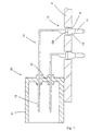
- the connector housing 20 is made of synthetic resin material and includes a rectangular hood part 21 open at a forward part (left side in Fig. 1) and a supporting wall part 22 which closes the rear end of the hood part 21.
- the metal terminals 10 are installed on the connector housing 20 by penetrating through the supporting wall part 22.
- the circuit substrate P is generally of electrically insulating material and has a printed circuit (not shown) formed on an upper surface thereof.
- the circuit substrate P has circular contact holes H (referred to below as installing holes) which perpendicularly penetrate the substrate.
- Each metal terminal 10 is inserted into the respective installing hole H from above.
- a contact region C continuous with the printed circuit is formed by plating the inner peripheral surface of the installing hole H with a metal. The metal terminal 10 is brought into contact with the contact region C.
- the elongate metal terminal 10 is made of a resiliently deformable electrically conductive metal which is bent in an L-shape.
- a tab part 11 of the metal terminal 10 penetrates horizontally through the supporting wall part 22.
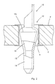
- a substrate connection section 12 of the metal terminal 10 bent vertically downward from the rear end of the tab section 11 is inserted through the installing hole H of the circuit substrate P.
- the substrate connection section 12 has an outer wall which defines a central cavity. To allow its radial (transverse) elastic deformation, the substrate connection section 12 has a slit 15 extending along the direction in which the section 12 is inserted into the installing hole H.
- the section 12 is, apart from the slit 15, symmetrical about an axis which is parallel to the insertion direction.
- the upper part of the section 12 includes a tapered connection part 13 whose diameter decreases gradually in the forward (insertion) direction, i.e. downwardly in Figs. 1 and 2, of the section 12.
- the maximum outer-diameter portion 13L of the tapered connection part 13 makes an elastic circumferential linear contact with the contact region C of the installing hole H.
- the outer peripheral surface of the tapered connection part at the widest position thereof (referred to here as the maximum outer-diameter portion 13L) has an outwardly convex surface, as seen in axial section.
- the outer diameter of the maximum outer-diameter portion 13L is larger than the inner diameter of the installing hole H.
- the minimum diameter of the tapered connection part 13 at its lower end is smaller than the inner diameter of the installing hole H.
- the substrate connection section 12 has a cylindrical leading part 14 extending from the lower end of the tapered connection part 13 to a tapered lower end. The outer diameter of the leading part 14 is smaller than the inner diameter of the installing hole H.
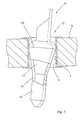
- the terminal 10 is made by punching and bending sheet metal having appropriate resilience in the shaped state.
- the substrate connection section 12 of each metal terminal 10 is inserted downward into the installing hole H.
- the leading part 14 penetrates the installing hole H, and then the tapered connection part 13 penetrates thereinto.
- the outer surface of the tapered connection part 13 contacts the upper surface of the substrate at the edge of the upper end of the installing hole H. As a result, the tapered connection part 13 is contracted elastically and its diameter decreases.
- the inclination of the outer surface of the tapered connection part 13 that contacts the upper edge is small relative to the insertion direction of the metal terminal 10.
- the tapered connection part 13 contracts smoothly without being snagged by the upper edge.
- the metal terminal 10 has a low insertion resistance.
- the connector housing 20 When the connector housing 20 has been fixed to the upper surface of the circuit substrate P, the operation of inserting the metal terminal 10 into the installing hole H is completed. It is to be noted that the metal terminal 10 is not soldered to the inner surface of the installing hole H.
- the maximum outer-diameter portion 13L of the tapered connection part 13 bears elastically on the contact region C of the inner surface of the installing hole H.
- the metal terminal 10 makes electrical contact with the contact region C with a predetermined contact pressure. As shown in Fig.
- the maximum outer-diameter portion 13L of the tapered connection part 13 makes a linear contact with the contact region C with a contact pressure which is approximately uniform around the entire circumference of the maximum outer-diameter portion 13L. Further, because the tapered connection part 13 bears elastically on the inner surface of the installing hole H, the metal terminal 10 can be prevented from moving radially relative to the axis of the installing hole H.
- the substrate connection section 12 of the metal terminal 10 is pulled out from the installing hole H, with the connector housing 20 being lifted above the circuit substrate P.
- the outer surface of the tapered connection part 13 makes sliding contact with the edge of the upper end of the hole H, with the tapered connection part 13 being restored to its original state as its diameter increases.
- the elastic restoring force of the tapered connection part 13 urges the metal terminal 10 in the withdrawal direction, thus accelerating the withdrawal.
- the outer surface of the cylindrical part separates from the inner surface of the installing hole when the metal terminal is inclined with respect to the axis of the installing hole.
- the outer surface of the cylindrical part may make only two-point contact, i.e. with the upper and lower edges of the installing hole.
- the metal terminal 10 of the first embodiment does not have this disadvantage.
- the metal terminal 10 contacts the inner surface of the installing hole H, with the maximum outer-diameter portion 13L of the tapered connection part 13 making the circumferential linear contact with the inner surface of the installing hole H.
- the maximum outer-diameter portion 13L maintains linear contact around the entire circumference of the inner peripheral surface of the installing hole H, the tapered connection part 13 being slightly deformed into an elliptical cross-section. Accordingly, the metal terminal 10 and the contact region C are capable of maintaining the intended contact state.
- a displacement of the contact line between the outer surface of the maximum outer-diameter portion 13L and the inner surface of the installing hole H occurs when the metal terminal 10 inclines with respect to the axis of the installing hole H.
- the maximum outer-diameter portion 13L of the tapered connection part 13 is not angular but has an outwardly convex surface, there is less possibility that the metal terminal 10 damages the contact region C on the inner surface of the installing hole H.
Landscapes
- Engineering & Computer Science (AREA)
- Manufacturing & Machinery (AREA)
- Microelectronics & Electronic Packaging (AREA)
- Coupling Device And Connection With Printed Circuit (AREA)
Claims (2)
- Substrat (P) für eine elektrische Schaltung bzw. einen elektrischen Schaltkreis, wobei das Substrat (P) ein kreisförmiges Kontaktfenster bzw. Kontaktloch (H) aufweist, in das ein metallischer Anschluß (10) eingesetzt ist, der elektrischen Kontakt mit einer Innenfläche des Kontaktlochs (H) ergibt bzw. bildet,
wobei der metallische Anschluß einen Einsetzbereich (12) mit einer elastisch verformbaren, äußeren Wand aufweist, die einen mittleren Hohlraum mit einem Schlitz (15) definiert, der sich entlang der äußeren Wand in der Einsetzrichtung des Anschlusses erstreckt und es dem Anschluß erlaubt, sich in der Querrichtung einzuengen bzw. einzuschnüren, und
wobei der Einsetzbereich (12) einen verjüngten Teil (13) aufweist, der einen weitesten Bereich des metallischen Anschlusses innerhalb des Kontaktloches ergibt und der in der Einsetzrichtung gleichmäßig enger wird,
dadurch gekennzeichnet, daß
sich die Außenumfangsfläche des verjüngten Teils an dem weitesten Bereich nachgiebig federnd an der Innenfläche des Kontaktloches entlang einer linearen Kontaktregion abstützt, so daß der metallische Anschluß in Bezug auf die Achse des Kontaktloches schrägstellbar bzw. neigbar ist, während eine lineare Kontaktregion aufrechterhalten wird. - Substrat für eine elektrische Schaltung bzw. einen elektrischen Schaltkreis nach Anspruch 1, bei dem die Außenumfangsfläche an dem weitesten Bereich nach außen konvex ist, wenn im Axialschnitt betrachtet.
Applications Claiming Priority (2)
| Application Number | Priority Date | Filing Date | Title |
|---|---|---|---|
| JP11199209A JP2001023716A (ja) | 1999-07-13 | 1999-07-13 | 端子金具 |
| JP19920999 | 1999-07-13 |
Publications (2)
| Publication Number | Publication Date |
|---|---|
| EP1069650A1 EP1069650A1 (de) | 2001-01-17 |
| EP1069650B1 true EP1069650B1 (de) | 2002-10-09 |
Family
ID=16403957
Family Applications (1)
| Application Number | Title | Priority Date | Filing Date |
|---|---|---|---|
| EP00305643A Expired - Lifetime EP1069650B1 (de) | 1999-07-13 | 2000-07-05 | Metallkontakt |
Country Status (4)
| Country | Link |
|---|---|
| US (1) | US6340318B1 (de) |
| EP (1) | EP1069650B1 (de) |
| JP (1) | JP2001023716A (de) |
| DE (1) | DE60000557T2 (de) |
Families Citing this family (5)
| Publication number | Priority date | Publication date | Assignee | Title |
|---|---|---|---|---|
| JP2004503899A (ja) * | 2000-02-09 | 2004-02-05 | ソリッド ステート スタンピング インコーポレイテッド | コンプライアントピンとその製造方法 |
| DE102004030443A1 (de) * | 2004-06-24 | 2006-01-19 | Robert Bosch Gmbh | Steuergerät |
| JP5795907B2 (ja) * | 2011-08-29 | 2015-10-14 | 矢崎総業株式会社 | 基板コネクタ用の圧入端子およびその圧入端子のコネクタハウジングに対する固定構造 |
| JP5541305B2 (ja) * | 2012-03-16 | 2014-07-09 | 第一精工株式会社 | プレスフィット用コネクタ端子 |
| KR102421781B1 (ko) * | 2015-02-25 | 2022-07-15 | 삼성디스플레이 주식회사 | 핀 구조물, 및 핀 구조물을 포함하는 커넥터 |
Family Cites Families (12)
| Publication number | Priority date | Publication date | Assignee | Title |
|---|---|---|---|---|
| US4017143A (en) | 1975-12-16 | 1977-04-12 | Litton Systems, Inc. | Solderless electrical contact |
| US4526429A (en) * | 1983-07-26 | 1985-07-02 | Augat Inc. | Compliant pin for solderless termination to a printed wiring board |
| US4752250A (en) * | 1985-02-05 | 1988-06-21 | American Specialties Corp. | Compliant connector |
| JPS62271376A (ja) * | 1986-01-31 | 1987-11-25 | デイジタル イクイプメント コ−ポレ−シヨン | 回路板連結用プレス嵌めピン |
| US5160270A (en) * | 1989-06-13 | 1992-11-03 | General Datacomm, Inc. | Integrated circuit packages using tapered spring contact leads for direct mounting to circuit boards |
| US5215471A (en) * | 1989-06-13 | 1993-06-01 | General Datacomm, Inc. | Electrical connectors having tapered spring contact elements for direct mating to holes |
| US5002507A (en) * | 1990-01-31 | 1991-03-26 | E. I. Du Pont De Nemours And Company | Circuit board contact element and compliant section thereof |
| US5154621A (en) * | 1991-07-29 | 1992-10-13 | Zierick Manufacturing Corporation | Printed circuit board contact system |
| US5169322A (en) * | 1991-11-04 | 1992-12-08 | Amp Incorporated | Receptacle header of low height for connector to multiple pins |
| US5199908A (en) * | 1992-07-16 | 1993-04-06 | Amp Incorporated | Electrical contact |
| US5509814A (en) * | 1993-06-01 | 1996-04-23 | Itt Corporation | Socket contact for mounting in a hole of a device |
| US6098281A (en) * | 1996-11-06 | 2000-08-08 | Weidmuller Interface Gmbh & Co. | Electrical pins and method for their insertion into apertures of a circuit board |
-
1999
- 1999-07-13 JP JP11199209A patent/JP2001023716A/ja active Pending
-
2000
- 2000-07-05 EP EP00305643A patent/EP1069650B1/de not_active Expired - Lifetime
- 2000-07-05 DE DE60000557T patent/DE60000557T2/de not_active Expired - Fee Related
- 2000-07-13 US US09/616,370 patent/US6340318B1/en not_active Expired - Fee Related
Also Published As
| Publication number | Publication date |
|---|---|
| EP1069650A1 (de) | 2001-01-17 |
| DE60000557D1 (de) | 2002-11-14 |
| JP2001023716A (ja) | 2001-01-26 |
| DE60000557T2 (de) | 2003-06-18 |
| US6340318B1 (en) | 2002-01-22 |
Similar Documents
| Publication | Publication Date | Title |
|---|---|---|
| EP1686660B1 (de) | Gegenüber der Umgebung abgedichteter selbstzentrierender Verbinder | |
| US10535942B2 (en) | Spring connector | |
| US7374432B2 (en) | Connector | |
| US5562480A (en) | Electrical connecting device | |
| US5401180A (en) | Connector shorting spring | |
| JP2002042994A (ja) | 同軸ケーブルをプリント基板カードへ接続するための装置 | |
| EP2700128B1 (de) | Anschlussstück | |
| KR20130118257A (ko) | 전기 커넥터 | |
| US6135816A (en) | Electrical connector having an improved construction for fixing shield plates to a receptacle connector | |
| US20260039049A1 (en) | Connector | |
| US9673542B1 (en) | Poke-in electrical connector having a contact with a base extending through an opening in a bottom of a housing | |
| US20070293100A1 (en) | Pin For The Soldering-Free Electric Connection To A Printed Circuit Board, A Pressing-In Tool, In Addition To A Method For The Production Of A Soldering-Free Electric Connection | |
| EP0794596A2 (de) | Steckverbindungsmodul, Steckverbindungsmodulkit und Zusammenbau von Steckverbindungsmodul und Platte | |
| JP3361757B2 (ja) | プレスインコンタクト | |
| CN111370897B (zh) | 一种电连接装置 | |
| JP2001015228A (ja) | 基板用グランドピン付きコネクタ | |
| JP3297397B2 (ja) | 圧入端子及びこれを有する電気コネクタ | |
| EP1069650B1 (de) | Metallkontakt | |
| EP3629423B1 (de) | Elektrischer verbinder mit in der kontakthöhle integrierter kunststofflasche | |
| US20070155227A1 (en) | Electrical connector | |
| JP6549210B2 (ja) | 車両用アンテナ装置に用いるケーブル接続構造 | |
| US12512611B2 (en) | Connector for connecting an electrical termination on a printed circuit, corresponding assembly methods | |
| EP0692149B1 (de) | Elektrischer verbinder | |
| US11296438B1 (en) | Electrical connector assembly having a terminal-less connection system | |
| EP4510388A1 (de) | Elektrisches verbindungssystem für elektrofahrzeuge |
Legal Events
| Date | Code | Title | Description |
|---|---|---|---|
| PUAI | Public reference made under article 153(3) epc to a published international application that has entered the european phase |
Free format text: ORIGINAL CODE: 0009012 |
|
| 17P | Request for examination filed |
Effective date: 20000726 |
|
| AK | Designated contracting states |
Kind code of ref document: A1 Designated state(s): DE FR GB IT Kind code of ref document: A1 Designated state(s): DE |
|
| AX | Request for extension of the european patent |
Free format text: AL;LT;LV;MK;RO;SI |
|
| 17Q | First examination report despatched |
Effective date: 20010611 |
|
| AKX | Designation fees paid |
Free format text: DE FR GB IT |
|
| GRAG | Despatch of communication of intention to grant |
Free format text: ORIGINAL CODE: EPIDOS AGRA |
|
| GRAG | Despatch of communication of intention to grant |
Free format text: ORIGINAL CODE: EPIDOS AGRA |
|
| GRAG | Despatch of communication of intention to grant |
Free format text: ORIGINAL CODE: EPIDOS AGRA |
|
| GRAH | Despatch of communication of intention to grant a patent |
Free format text: ORIGINAL CODE: EPIDOS IGRA |
|
| GRAH | Despatch of communication of intention to grant a patent |
Free format text: ORIGINAL CODE: EPIDOS IGRA |
|
| RBV | Designated contracting states (corrected) |
Designated state(s): DE |
|
| GRAA | (expected) grant |
Free format text: ORIGINAL CODE: 0009210 |
|
| AK | Designated contracting states |
Kind code of ref document: B1 Designated state(s): DE |
|
| REF | Corresponds to: |
Ref document number: 60000557 Country of ref document: DE Date of ref document: 20021114 |
|
| PLBE | No opposition filed within time limit |
Free format text: ORIGINAL CODE: 0009261 |
|
| STAA | Information on the status of an ep patent application or granted ep patent |
Free format text: STATUS: NO OPPOSITION FILED WITHIN TIME LIMIT |
|
| 26N | No opposition filed |
Effective date: 20030710 |
|
| PGFP | Annual fee paid to national office [announced via postgrant information from national office to epo] |
Ref country code: DE Payment date: 20040715 Year of fee payment: 5 |
|
| PG25 | Lapsed in a contracting state [announced via postgrant information from national office to epo] |
Ref country code: DE Free format text: LAPSE BECAUSE OF NON-PAYMENT OF DUE FEES Effective date: 20060201 |