EP1048190B1 - Ballast electronique pour lampe a decharge - Google Patents
Ballast electronique pour lampe a decharge Download PDFInfo
- Publication number
- EP1048190B1 EP1048190B1 EP98964410A EP98964410A EP1048190B1 EP 1048190 B1 EP1048190 B1 EP 1048190B1 EP 98964410 A EP98964410 A EP 98964410A EP 98964410 A EP98964410 A EP 98964410A EP 1048190 B1 EP1048190 B1 EP 1048190B1
- Authority
- EP
- European Patent Office
- Prior art keywords
- circuit
- lamp
- gas discharge
- electronic ballast
- control circuit
- Prior art date
- Legal status (The legal status is an assumption and is not a legal conclusion. Google has not performed a legal analysis and makes no representation as to the accuracy of the status listed.)
- Expired - Lifetime
Links
Images


Classifications
-
- H—ELECTRICITY
- H05—ELECTRIC TECHNIQUES NOT OTHERWISE PROVIDED FOR
- H05B—ELECTRIC HEATING; ELECTRIC LIGHT SOURCES NOT OTHERWISE PROVIDED FOR; CIRCUIT ARRANGEMENTS FOR ELECTRIC LIGHT SOURCES, IN GENERAL
- H05B41/00—Circuit arrangements or apparatus for igniting or operating discharge lamps
- H05B41/14—Circuit arrangements
- H05B41/26—Circuit arrangements in which the lamp is fed by power derived from dc by means of a converter, e.g. by high-voltage dc
- H05B41/28—Circuit arrangements in which the lamp is fed by power derived from dc by means of a converter, e.g. by high-voltage dc using static converters
- H05B41/295—Circuit arrangements in which the lamp is fed by power derived from dc by means of a converter, e.g. by high-voltage dc using static converters with semiconductor devices and specially adapted for lamps with preheating electrodes, e.g. for fluorescent lamps
- H05B41/298—Arrangements for protecting lamps or circuits against abnormal operating conditions
- H05B41/2981—Arrangements for protecting lamps or circuits against abnormal operating conditions for protecting the circuit against abnormal operating conditions
Definitions
- the present invention relates to an electronic ballast for operation at least one fluorescent or gas discharge lamp according to the preamble of Claim 1.
- Such an electronic ballast is for example from EP-B1-0338 109 known.
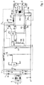
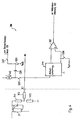
- Fig. 10 shows the basic structure of this electronic ballast.
- the electronic ballast shown in FIG. 10 first comprises a circuit A, which is connected to the AC network.
- This circuit A serves as an RF harmonic filter to reduce the harmonic harmonics of the mains frequency as well for radio interference suppression.
- the circuit A is followed by a rectifier circuit B which supplies the mains voltage converted into a rectified intermediate voltage and this via a harmonic filter C, which serves to smooth the intermediate voltage, an inverter circuit D supplies.
- This inverter D serves as a controllable AC voltage source and converts the DC voltage of the rectifier B into a variable AC voltage.
- the inverter D generally comprises two controllable switches (not shown), for example MOS field effect transistors.
- the two switches are in the form of a Half-bridge circuit interconnected and are using an appropriate Bridge driver alternately controlled such that one of the switches on and one other is off.
- the two inverter switches are connected in series connected between a supply voltage and ground, being at the common Node between the two inverter switches a load circuit or Output circuit E is connected in which a gas discharge lamp or Fluorescent lamp G is arranged.
- This output circuit E includes one Series resonance circuit via which the "chopped" high-frequency AC voltage of the Inverter D of the fluorescent lamp G is supplied.
- the Lamp electrodes of the fluorescent lamp G preheated to increase the lamp life extend.
- the preheating can, for example, with the help of a heating transformer take place, the primary winding is connected to the series resonance circuit, while the Secondary windings of the heating transformer coupled to the individual lamp filaments are. In this way it is possible to use the lamp filaments even in the ignited mode To supply energy.
- the frequency of the inverter D supplied AC voltage compared to the resonance frequency of the series resonance circuit of the output circuit E changed such that the applied to the gas discharge lamp G. Voltage does not cause the lamp to ignite.
- the electronic ballast has a control circuit F on, which monitors various circuit sizes of the electronic ballast and if a limit value is exceeded, a corresponding control signal for the Inverter D generates the frequency of those generated by the inverter D. AC voltage to change depending on the detected fault.
- the control circuit F, the lamp voltage, the preheating voltage Lamp operating current, the impedance phase angle of the output circuit E or that of Monitor the DC voltage generated by the rectifier B and the inverter frequency adjust so that the lamp voltage, the preheating voltage or the lamp current do not exceed a predetermined limit value that was taken from the rectifier B.
- DC power is as constant as possible or a capacitive operation of the series resonance output circuit E is avoided.
- a simple procedure for choosing a suitable lamp start is in the GB 2 053 592 A.
- the present invention is based on the object of the prior art improve known methods for selecting the type of lamp start and to ensure reliable functioning at the same time.
- the electronic ballast has a control circuit which or operating size of the electronic ballast is monitored and dependent on the value of this circuit size, the electronic ballast either with a Operates preheating or without preheating.
- the electronic Ballast is designed such that it automatically when a new or Restart detects whether the correspondingly controlled gas discharge lamp previously was already in operation, so that the lamp electrodes may need to be preheated Gas discharge lamp can be dispensed with.
- the control circuit detects when the electronic ballast automatically one of those in the energy storage circuit remaining charge corresponding voltage - this being a measure of the
- the electronic ballast is switched off - and compares it with the help of Comparator means with a reference value. Is the at the time of restart of the electronic ballast still high enough charge controls the Control circuit on the gas discharge lamp without preheating. Otherwise, a Preheating operation carried out.
- the energy storage circuit for example by a the control circuit connected RC element can be formed during operation charged to a predetermined (fixed) supply voltage potential.
- the control circuit Output signal of the state hold circuit for the commissioning of the Evaluates gas discharge lamp.
- charging the energy storage circuit has a predetermined and thus known supply voltage potential as a result that temporal behavior of the monitored circuit size fully known and from external influences as well as possible dimming settings of the lamp at the time of the Switching off the ballast is independent.
- temporal behavior of the monitored circuit size fully known and from external influences as well as possible dimming settings of the lamp at the time of the Switching off the ballast is independent.
- it is possible to design the circuit so that after a certain predetermined switch-off time the lamp regardless of the to this In any case, the present coil temperature started with preheating mode becomes.
- a corresponding standard which always starts with a lamp after a switch-off period of more than 400 ms Preheat operation requires to be met.
- the second advantage of the circuit according to the invention is that it ensures is that the evaluation of the comparison result only during the lamp start a change in the output signal is carried out at a later time however, it has no influence on further operations.
- the Gas discharge lamp can be put into operation as quickly as possible by clicking on one unnecessary preheating mode is dispensed with.
- the lamp electrodes of the gas discharge lamp are protected because they are excessive Heating of the lamp electrodes is also prevented. This ensures that sufficient even when the gas discharge lamp is started up without preheating Temperature of the lamp electrodes for igniting the gas discharge lamp is present.
- the electronic ballast shown in FIG. 1 first comprises a circuit A, which on the input side to a supply voltage, for example a mains voltage, is connected and used for radio interference suppression.
- Circuit A is in the usual way constructed and includes, for example, capacitive input filters and possibly. Harmonic chokes.
- a capacitor C2 and a are only exemplary Symmetry transformer L1 shown, with a surge arrester or a VDR with the designation F1 can be connected in parallel.
- the circuit B following the circuit A comprises one Full wave rectifier bridge with diodes V1 - V4.
- the rectifier circuit B converts the supply AC voltage present on the input side into a rectified one Intermediate voltage around.
- the rectifier circuit B can therefore be omitted if that electronic ballast is operated with DC voltage.
- the following circuit part C is used for harmonic filtering and smoothing of the intermediate voltage supplied to the rectifier B.
- the circuit C shown in Fig. 1 includes, for example, capacitors C3, C11, a diode V5, a coil L2, one MOS field-effect transistor T1 and an integrated circuit Control circuit IC1.
- the control circuit IC1 is at a supply voltage potential VCC connected and can be connected to the other circuit elements in such a way that it receives different voltage potentials U or currents I.
- the one in Fig. 1 The structure of the circuit C shown is of course to be understood purely as an example.
- an inverter circuit D controlled as the essential elements two in series between one Supply voltage line and ground switched controllable switches, in the present Example in the form of MOS field effect transistors T2 and T3.
- the two Inverter switches T2, T3 are connected to form a half bridge and are each controlled with the aid of a control circuit IC2 designed as an integrated circuit, i.e. opened and closed.
- the control circuit IC2 thus also takes over Function of a bridge driver and is connected to a corresponding one Supply voltage line VCC connected or coupled to it.
- the Inverter circuit D generates depending on that of rectifier circuit B. generated rectified intermediate voltage an AC voltage with variable Frequency and / or duty cycle.
- the inverter D is in the usual way built and its function is well known, so here on another Explanation can be omitted. It is only important at this point that the Control circuit IC2 the two depending on the control signals supplied Inverters T2 and T3 control alternately, so that at the connection point a "chopped", high-frequency between the two inverter switches T2 and T3 AC voltage occurs.
- the load circuit E is for the connection of two Gas discharge lamps G1, G2 designed in tandem configuration. Of course leaves load circuit E also change in such a way that only one gas discharge lamp or more than two gas discharge lamps can be operated.
- the load circuit E is a series resonance circuit consisting of a Has resonant circuit coil L3 and a resonant circuit capacitor C14.
- This Series resonance circuit or resonance circuit coil L3 is at the connection point connected between the two inverter switches T2 and T3 and the Resonant circuit capacitor C14 is arranged to be parallel to that operating gas discharge lamp or the gas discharge lamps G1, G2 to be operated is switched.
- the high-frequency AC voltage generated by the inverter D. is supplied to the gas discharge lamps G1 and G2 via the series resonance circuit.
- the two are Gas discharge lamps G1 and G2 in tandem configuration to the load circuit E or that electronic ballast connected.
- the ignition voltage to the gas discharge lamps G1, G2 these are preheated to extend the life of the gas discharge lamps.
- a heat exchanger L4 is provided whose primary winding is in Series is connected to the resonant circuit capacitor C14, while the Secondary winding, the lower filament of the upper gas discharge lamp G1 and the upper one Helix of the lower gas discharge lamp G2 connects.
- preheating mode becomes the frequency of the AC voltage supplied by the inverter E. the resonance frequency of the series resonance circuit set such that the above Resonant circuit capacitor C14 and thus across the gas discharge lamps G1 and G2 applied voltage does not cause ignition of the gas discharge lamps.
- the capacitor C15 shown in FIG. 1 adapts the Preheating voltage in the tandem configuration shown in Fig. 1 Gas discharge lamps G1 and G2.
- the electronic shown in Fig. 1 goes Ballast in the actual operating phase, in which the frequency of the Inverter D supplied AC voltage continuously, for example is set that a constant as possible by the gas discharge lamps G1, G2 Lamp current flows or a constant as possible on the gas discharge lamps Lamp voltage is present. As will be explained in more detail below, this is shown in FIG.
- a circuit module serves as the heart the previously mentioned control circuit IC2 and several external components as external circuitry of the control circuit IC2 comprises.
- the main external Components are six resistors R10, R13 - R16 and R21, R22 and two Capacitors C7 and C17. As shown in Fig. 1, the individual are external Components connected to respective input connections of the control circuit IC2.
- the External components connected to the control circuit IC2 serve primarily for Detection of certain circuit sizes of the electronic ballast, so that this can be evaluated in the control circuit IC2.
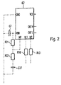
- FIG. 2 shows an enlarged illustration of the control circuit IC2 shown in FIG. 1 as well as the external wiring of the individual input connections of the control circuit IC2. 2 are only the essential connections and external components shown.
- the control circuit IC2 is advantageously as application specific integrated circuit, ASIC) and in a multi-pole SMD housing (Surface Mounted Device) accommodated.
- the control circuit IC2 is both for operation of an individual lamp output circuit E and also for the operation of one for one in FIG. 1 Tandem configuration shown with several gas discharge lamps designed load circuit E suitable.
- the Control circuit IC2 several connections, which have the following functions.
- To the Connection GND is the reference potential, i.e. the ground potential, for the individual analog and Digital function blocks of the control circuit IC2 created. 1 shows that the ground potential of the entire electronic ballast over a Coupling capacitor C1 is grounded.
- At the connection VDD, which over the Coupling capacitor C7 is connected to the ground potential (see. Fig. 1), the internal generated supply voltage for the individual analog and digital function blocks of the Control circuit IC2 provided.
- the NP connection serves, as will be explained in more detail below for external setting and detection of the preheating method, i.e. to Selection between a cold start and warm start operation.
- connection NP connected externally in such a way that a dynamic choice of the preheating method is possible.
- the connection VL1 is detected via those shown in FIG. 1 and partly in FIG. 2 Resistors R10 and R14, R15 divided the lamp voltage of the Gas discharge lamps G1, G2 and thus primarily serves Lamp voltage monitoring.
- the connection ILC is used analogously with the aid of FIG. 1 and resistors R13 and R16 shown partially in Fig. 2 for monitoring the Output circuit or load circuit current (choke current) or for monitoring the through the gas discharge lamps G1, G2 after their ignition flowing lamp current by with the help of the shunt resistor R16 a voltage proportional thereto and the Control circuit is supplied via the connection ILC.
- connection VL1 thus serves for voltage monitoring, while the ILC connection is used for current monitoring.
- the Both output connections OUTL and OUTH serve to control the one in FIG. 1 shown low or high half-bridge switch T3 or T2.
- TTL level control signals at the output connections OUTL and OUTH for switching the two inverter switches T2 and T3 on and off provided.
- the connection VCC of the control circuit IC2 is finally the central one Supply voltage connection of the control circuit IC2.
- the supply voltage range can include 10-18V, for example. Furthermore controls the control circuit IC2, the inverter switches T2 and T3 such that from the inverter circuit D an AC voltage of variable frequency on the output side is generated with an operating frequency range of 40-80 kHz, for example.
- the control circuit IC2 forms the heart of the whole shown in FIG. 1 electronic ballast and therefore includes a variety of different Functions.
- the preheating method for the connected gas discharge lamp (s) dynamically defined and between a cold start and a warm start operation can be changed.
- the control circuit IC2 for a defined preheating operation with a defined one Preheating time and a defined preheating current.
- the control circuit IC2 also ensures a predefined ignition operation with a specified ignition time and a specified Ignition voltage.
- the connections ILC or VL1 of the control circuit IC2 can for example the preheating current and the lamp operating current or the lamp voltage recorded and regulated to a constant value as possible.
- a capacitive operation of the Load circuit E monitors.
- the occurrence can also occur via the voltage connection VL1 of a constant light effect in a connected gas discharge lamp G1, G2 recognized become.
- the occurrence of a Gas defect which leads to an overvoltage on the corresponding gas discharge lamp leads, recognized and accordingly the electronic ballast in this case be switched off.
- a special function of the control circuit IC2 is recognition a lamp change, the. In the tandem configuration shown in FIG Lamp change detection is in particular independent of the changed lamp, i.e. both the upper gas discharge lamp G1 and the lower one can be changed Gas discharge lamp G2 can be detected.
- control circuit IC2 preferably digitally implemented sequence control implemented, which ensures that the gas discharge lamp (s) connected to the electronic ballast in accordance with predetermined operating states are controlled, with an operating state in a new operating state only if at least one specific condition is met can be changed.
- IC2 preferably digitally implemented sequence control implemented, which ensures that the gas discharge lamp (s) connected to the electronic ballast in accordance with predetermined operating states are controlled, with an operating state in a new operating state only if at least one specific condition is met can be changed.
- IC2 preferably digitally implemented sequence control implemented, which ensures that the gas discharge lamp (s) connected to the electronic ballast in accordance with predetermined operating states are controlled, with an operating state in a new operating state only if at least one specific condition is met can be changed.
- IC2 preferably digitally implemented sequence control implemented, which ensures that the gas discharge lamp (s) connected to the electronic ballast in accordance with predetermined operating states are controlled, with an operating state in a new operating state only if at
- control circuit has IC2 other functions, all of which are given below with reference to the attached Drawing to be explained in more detail.
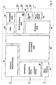
- Fig. 3 shows a block diagram of the internal structure of the previously described Control circuit IC2.
- a module 100 is initially coupled to the power connection ILC, which among other things to the previously explained current detection and capacitive current detection of the Load circuit serves.
- the evaluation of the current sensed via the connection ILC takes place in particular with the aid of a controller formed by a comparator circuit. To the To keep circuit complexity really low, this comparator circuit will also do that received by the voltage terminal VL1 of the control circuit IC2 and by one Module 200 supplied and evaluated voltage signal.
- the module 200 serves in particular for detecting the lamp voltage, for rectifying effect detection and for lamp change detection.
- the NP connection is another module 300 coupled, which to detect the warm or cold start operation during preheating the gas discharge lamp (s) to be controlled and to implement a dynamic one Preheating is used.
- a Voltage regulator module 400 connected, which has an internal voltage regulator, which is a regulated, very precise voltage for the power supply of all internal Provides function blocks.
- Another module 500 serves as a source for all required reference quantities, i.e. Reference voltages and reference currents in which Control circuit IC2.
- An oscillator 600 serves as an internal clock of the control circuit IC2, a time base generator 700 coupled to it depending on the predetermined one Clock of the oscillator 600 internal time variables for the sequential control of the Control circuit IC2, e.g.
- Another module 800 is used to implement the sequential control of the individual operating states of the entire electronic ballast and works closely with another module 900, which is used for measuring phase control.
- the module 900 is used in particular for event-filtered evaluation of certain error quantities of the electronic Ballast and for measuring phase-dependent control of all switches individual function blocks of the control circuit IC2.
- the sequencer 800 evaluates the event-filtered status messages from the measuring phase controller 900 and controls depending on the time variables specified by the time base generator 700 individual operating states of the electronic ballast or the control circuit IC2.
- the control circuit IC2 assigns a further module 1000 Inverter control on. With the help of this module 1000 the Measuring phase control 900 delivered frequency setting signals into corresponding Control signals for the upper inverter switch (via the output connection OUTH) or the lower inverter switch (via the output connection OUTL).
- the control circuit IC2 can be implemented both analog and digital Function blocks include.
- the digital part comprises the ASIC trained control circuit IC2, the time base generator 700, the sequencer 800, the measuring phase control 900 and the inverter control 1000.
- the control circuit IC2 be equipped such that the digital part with respect to Space requirement of the control circuit IC2 corresponds to the analog part.
- FIG. 4 shows a detailed circuit diagram of the current detection module shown in FIG. 3 100.
- Fig. 4 are also the external with the power connector ILC of the control circuit connected resistors R13 and R16, which are also shown in FIG. 1.
- a reference current Iref1 is added to the signal detected at the current connection ILC, to ensure that the signal to be processed by the current sensing module 100 is always in the working voltage range of the control circuit.
- an integrator circuit 105 is provided for integration of the input signal fed to it.
- the entire functional block 105 is such realizes that the integrator function both for measuring the lamp current (via the Connection ILC) in normal operation, as well as for rectification effect detection (via the Connection VL1) can be used.
- the integrator circuit 105 may have sample and hold elements, which alternately each Period of the internal clock generator (cf. module 600 in FIG. 3) the input signal of the Scan integrators. The charge thus stored in the sample and hold members turns on an integration amplifier of the integrator circuit 105. This process is repeated cyclically.
- the integrator 105 may have an internal controllable switch that does the above bridged sample and hold bridges and during the duration of the offset adjustment of the Integrators 105 is closed. This way, any signal, in particular the signal present at the input connection ILC via the switch S105 or a reference voltage potential for rectification effect detection from the voltage block 200 via switch S107, during the initialization phase on the actual Integration amplifier can be created.
- the actual integration amplifier of the integrator 105 has the task of Integrate the current measurement signal at the ILC connection in a precisely controlled time. In the case, that the current measurement signal present at the ILC connection from the integration amplifier Integrator circuit 105 is integrated, the switch S105 is closed, while for the case of the rectification effect evaluation that supplied via the switch S107 Reference potential for the rectification effect evaluation at the integrator circuit 105 is applied.
- a comparator 103 serves as the actual controller, which performs the required setpoint / actual value comparison performs and is connected to the output integrators 105.
- this comparator 103 shown in FIG. 4 makes it possible to use the comparator 103 very flexible to use.
- a switch S124 can use different comparator voltages or reference values to the comparator 103 can be added or applied, reference voltages being exemplary in FIG. 4 Vref1 - Vref6 are shown.
- the reference potential corresponds to Vref1 and Vref2 for example a desired preheating voltage during a Vor carving worriessShes.
- the controllable switch S124 the reference voltage Vref1 or Vref2 to the comparator 103 created so that the currently present on the ILC connector and not integrated Measuring signal is compared with the reference value Vref1 or Vref2 respectively applied.
- the reference potential Vref3 corresponds to that Integration start value of the integration amplifier of the integrator 105, so that when concerns of this reference potential Vref3, the comparator 103 real changes the Integration result can capture.
- the reference potentials Vref4 or Vref6 can a positive or negative limit for the supplied via switch S107 and correspond to the integrated lamp voltage of the connection VL1, so that by Comparison with these two limit values when the integration result is exceeded the occurrence of a rectification effect reliably in positive or negative direction to be able to recognize.
- the further reference potential Vref5 used which is switched on in the rectification effect detection and the Output or start value for the integration of those supplied via switch S107 Lamp voltage corresponds.
- the reference potentials Vref3 or Vref5 predetermined start values of the integration amplifier of the integrator 105 can thus, with the aid of the comparator 103, actually be relative to the corresponding one Starting value of the change in the corresponding integration variable determined become.
- the output signal of the comparator 103 becomes that shown in FIG. 3 Measuring phase control 900 supplied, which evaluates this and depending on the current measurement phase evaluated differently. This is how the measuring phase control ensures 900 for example for a corresponding adjustment of the output frequency of the Inverter of the electronic ballast, if that of the comparator 103 monitored current measurement signal of the connection ILC from the specified setpoint Vref3 differs.
- the measurement phase control an event-filtered signal, which indicates whether there is a rectification effect in a connected gas discharge lamp or Not. This signal is provided by the flow control block 800 shown in FIG. 3 evaluated and for operating state control of the entire electronic Ballast used.
- the measurement signal present at the connection ILC can also be under Bypassing the integrator circuit 105 are monitored and evaluated, e.g. one capacitive operation of the load circuit of the electronic ballast to detect.
- a detector for detecting a capacitive current flowing in the load circuit be provided, for example, the phase angle of the load circuit, i.e. the Phase difference between the load circuit voltage and the load circuit current, determined (Kapazitivstromer extended).
- the result of this monitoring or evaluation can be fed to the measuring phase controller 900.
- FIG. 5 a shows an enlarged illustration of the essential elements of the one already in FIG. 1 shown inverter D and the load circuit E.
- Fig. 5a assumed that only one gas discharge lamp G1 connected.
- 5a shows the two inverter switches connected in series T2 and T3 shown.
- the load circuit with its Series resonant circuit at the connection point between the two Inverter switches T2 and T3 connected, i.e. the resonance circuit coil L3 is with the resonant circuit capacitor C14 in parallel with the lower inverter switch T3 connected.
- the resonant circuit capacitor C14 is also parallel to that Gas discharge lamp G1 connected.
- free-wheeling diodes V11 and V12 are connected in parallel to protect the respective Serve as an inverter switch.
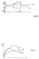
- 5b shows on the one hand the switch-on states of the two inverter switches T2 and T3 as well as the current profile of the current I L3 flowing through the choke L3 and the time profile of the voltage potential V L occurring at the connection point between the two inverter switches T2 and T3.
- a current flows in the freewheeling diode of the inverter switch to be switched on and the inverter half bridge switches the resonant load circuit inductively, ie the voltage or potential V L leads the choke current I L3 .
- the capacitive switching of the resonance load of the resonance load circuit is the capacitive switching of the resonance load of the resonance load circuit.
- FIG. 5a shows the course of the individual currents I 1 -I 4 that occur during the time intervals t 1 -t 4 shown in FIG. 5b in the case of an inductive or capacitive inductor current I L3 .
- the above-mentioned phenomenon occurs in particular at load circuit voltages V L with an output frequency close to the resonance frequency of the series resonance circuit, which is particularly the case when the gas discharge lamp G1 is ignited, with an inductive current initially flowing in the load circuit which leads to heating of the coil L3 leads. Due to the heating of the coil L3, its inductance decreases, so that a transition suddenly occurs from the inductive area to the faulty capacitive area.
- the height of the current amplitude at the time the lower one is switched on Inverter switch T3 detected because in this case the polarities of the to be detected Measured values favorable for processing within the ASIC Control circuit IC2 are. If the detected current value is below that by the corresponding reference potential predetermined limit value, is based on the presence of a capacitive operation of the load circuit closed, and there can be an output signal with are generated at a high level, which is shown in FIG Measurement phase control block 900 evaluated and finally from that also in FIG. 3rd inverter control block 1000 shown in drive signals for the two Inverter switches T2 and T3 are implemented with an increased frequency alternately switched on and off to increase the working frequency and thus to counteract capacitive operation.
- FIG. 6 shows the internal structure of the voltage detection block 200 and the external one coupled to terminal VL1 of voltage detection block 200 Wiring the control circuit.
- a series resistor R10 on the one hand with the connection VL1 and on the other hand with a voltage divider consisting of resistors R14 and R15 is coupled, the two voltage divider resistors R14 and R15 parallel to the Gas discharge lamp G1 or to those connected in tandem in FIG. 1 Gas discharge lamps G1 and G2 are switched.
- FIG. 6 assumed that, in contrast to FIG. 1, only one gas discharge lamp G1 is controlled, to which the resonant circuit capacitor C14 is also connected in parallel.
- the two resistors R14 and R15 have the task of acting on the gas discharge lamp G1 to divide the applied voltage so that with the help of the connection point between the resistors R14 and R15 attacking resistor R10 for the Lamp voltage representative measurement signal to the voltage terminal VL1 Voltage detection blocks 200 can be supplied.
- the three external resistors R10, R14 and R15 are advantageously variable, see above that - analogous to the power connection ILC (cf. resistors R13, R16) - via one Connection of the control circuit completely different from each other A total of three different control variables of the electronic ballast at times can be set or controlled using the same controller.
- setting the resistance values of the resistors R10, R14 and R15 can depending on the type of lamp currently being used or on the instant used electronic ballast the setpoints for the regulation of the three different control variables can be set or specified.
- the following sizes of the electronic ballast can be set: the maximum Lamp voltage positive / negative, the amplitude of the AC voltage component of the Lamp voltage signal and the signal increase of the lamp voltage signal for Rectifying effect evaluation.
- an internal reference current source is again provided, which the measuring signal present at the voltage connection VL1 with an additional internal Current Iref2 applied.
- the reference current Iref2 using the controllable switch S207 only activated during the evaluation of the rectification effect, i.e. closed. All other evaluations connected to the VL1 connection refer to the signal present at connection VL1 without additional reference current Iref2, i.e. without DC offset. Accordingly, during the rectification effect evaluation all other detectors on the VL1 connection deactivated, otherwise they are wrong would deliver results.
- gas discharge lamps occur due to wear and tear on the heating coil at the end of its service life
- Gas discharge lamps have the effect that the lamp electrodes change over time wear unevenly, i.e. the removal of the emission layers on the Lamp electrodes are different. Due to the different wear of the Lamp electrodes produce differences in the emissivity of the two Lamp electrodes. This has the consequence that when operating the corresponding Gas discharge lamp from one lamp electrode to another a higher current flows than vice versa. The course of the lamp current over time thus shows an excessive increase Half wave on.
- the previously explained rectification effect also has the consequence that the stronger worn electrode, which has a higher work function than the other electrode, heated up more than the other electrode when starting the gas discharge lamp.
- Work function is generally called the minimum energy required to solve a problem Electrons from a metal, in this case from a lamp electrode, required is.
- the heating of the lamp electrode described above can be particularly important in the case of lamps with a small diameter become so strong that parts of the lamp glass bulb melt can.
- each controlled lamp is switched on Occurrence of a rectification effect monitored so that when a Rectification effect can be reacted accordingly.
- the switch S207 shown in FIG. 6 is advantageously switched on some time before expected zero crossing of the lamp voltage signal present at connection VL1 closed, so that transients caused by the capacitor C201 Cannot additionally falsify the measurement signal. Exactly to the calculated zero crossing of the Lamp voltage, switch S201 is opened again. That on the in Figs. 4 and 6th Switch S107 signal shown corresponds at this time to AC voltage amplitude at terminal VL1, while the DC component of the switch S107 applied signal corresponds to the added reference voltage Vref8. By Finally, as previously explained, closing switch S107 will thus prepared measurement signal of the connection VL1 that shown in Fig. 4 Integrator circuit 105 supplied.
- the switching state of the switch S107 will be as well all other controllable switches of the entire control circuit IC2 from that in FIG. 3 phase control 900 shown controlled.
- the individual switches shown in Fig. 4 are closed or opened by the measuring phase control 900 in such a way that with With the aid of the comparator 103 an averaged over the upstream integrator circuit Evaluation of the current measurement signal present at the ILC connection or that at the connection VL1 applied voltage measurement signal is possible.
- the comparator can also 103 by corresponding actuation of the controllable switches of the one shown in FIG. 4
- Current detection blocks 100 also directly bypassing the integrator circuit with the Current measurement connection ILC are connected to the peak value of the current measurement signal evaluate or regulate at the ILC connection.
- the measurement phase control 900 which of the measurement or control states is assumed.
- That realized in the present control circuit IC2 Rectifier effect detection principle provides that the voltage connection VL1 detected lamp voltage using the integrator circuit of the one shown in FIG Current detection blocks 100 integrated and then the deviation from one predetermined setpoint is evaluated. In particular, that of the lamp voltage corresponding measurement signal over a full period or a multiple of a full period integrated the lamp voltage and then the deviation of the Integration result evaluated from the original integration start value.
- the comparator 103 the integration start value by applying the corresponding reference potential Vref5 supplied.
- Vref5 can, for example 3.0V
- as a positive reference potential Vref4 a value of 4.0V and as negative reference potential Vref6 a value of 2.0V can be used.
- the output signal of the comparator shown in FIG. 4 in turn becomes the Measuring phase control 900 supplied, the one after detection of a rectification effect corresponding status message or error message to the one shown in FIG. 3 Sequence control 800 delivers.
- the Measurement phase control 900 an event-filtered revision of this error message by and ensures that only then will an error message indicating the rectification effect be sent to the Sequence control 800 is output if the rectification effect is prolonged Period occurs continuously.
- the measurement phase controller 900 only provides a rectification effect error message the sequencer 800 if 32 times from the comparator 103 shown in FIG a rectification effect is detected successively every 255th period of the lamp voltage.
- the occurrence of a rectification effect only taken into account in the operating state of the electronic ballast, because for example, during the preheating phase, the occurrence of a rectification effect is not Shutdown of the system.
- the Rectification effect detection in particular by the fact that during the individual half-waves the lamp voltage or the dependent clock pulse size (high-frequency) reference clock are counted and compared with each other, the counted clock pulses are dependent on the duration of the respective half-wave. If there is no rectification effect, they are correct during the positive and negative Half-waves counted clock pulses. If there is a rectification effect, give way on the other hand, the clock pulses counted during the positive and negative half-waves from each other.
- 11a shows a circuit implementation of this exemplary embodiment with an up / down counter 107, which receives a UZERO signal as the actual input signal and further receives a high-frequency reference clock signal CLK, for example with the frequency 10 MHz, as well as a reset or reset signal as control signals ,
- the signal UZERO assumes a positive and otherwise a negative voltage level during each positive half-wave of the lamp voltage present at the connection VL1 and thus detects the zero crossing of the lamp voltage.
- the counter 107 is started at the zero crossing of the lamp voltage and counts either up or down during the subsequent half-wave of the lamp voltage. If the measurement signal, ie the lamp voltage, reaches zero again after a half period, the counting direction of the counter 107 is reversed. After a full period of the lamp voltage has elapsed, the current counter reading N of the counter 103 is connected to a comparator which can be formed, for example, by the comparator 103 already described above. This comparator 103 compares the current counter reading N with the initialization value or the original counter reading of the counter 107. If there is no rectification effect, the counter reading N must have reached the output value N 0 again after the next zero crossing of the lamp voltage.
- the comparator 103 advantageously compares the counter reading N with the initial value N 0 within certain tolerance limits, in order not to prematurely conclude that there is a rectification effect.
- the output signal of the comparator 103 is fed via a D flip-flop 108 clocked by a latch signal to the measuring phase controller 900, which - as has been described above - evaluates this signal and in particular carries out an event-filtered evaluation, ie only then concludes that there is a rectification effect , if, for example, a rectification effect is reported by the comparator 103 32 times in succession every 255th period of the lamp voltage.
- the zero crossing signal UZERO can, for example, from a further comparator 203 originate the voltage measurement signal present at the voltage connection VL1 monitored for its zero crossing.
- this Zero voltage comparator 203 is the entire integrated measuring system Control circuit IC2 cyclically with respect to the zero point of the lamp voltage synchronized.
- the synchronization advantageously takes place every other period the output frequency.
- An exception to this principle is the Rectification effects evaluation. In this case, the synchronization is based on the Integration carried out for rectification effects evaluation over a full period of Lamp voltage delayed by two more periods.
- the output signal of the Zero crossing comparator 203 is also fed to measuring phase controller 900 and is of central importance for the control of all controllable switches entire control circuit, the actuation of each at the zero crossing of the Lamp voltage is controlled.
- FIG. 11 b shows a representation of the signal profiles in the circuit shown in FIG. 11 a in the absence of a rectification effect and the states that occur in the process.
- the zero crossing signal UZERO assumes the positive level during the positive half-wave of the lamp voltage U VL1 and the counter 107 decreases its counter reading N based on the initialization value N0 according to the reference clock CLK until the lamp voltage U VL1 passes through zero again , The counter reading N is then increased again.
- the latch signal After a period of the lamp voltage U VL1 , the latch signal outputs the output value of the comparator 103 to the measuring phase controller 900 via the D flip-flop 108, and then the counter 107 is reset to the initial value N 0 using the reset signal.
- the counter reading N of the counter 107 again corresponds to the output value N 0 , so that the comparator 103 reports no rectification effect.
- 11c and 11d show courses of the counter reading N if there is a rectification effect, the counter reading N being greater than N 0 according to FIG. 11c or smaller than N 0 according to FIG thus the comparator 103 recognizes and reports the rectification effect by comparing N with N 0 .
- the comparison of the comparator N advantageously takes place within predetermined tolerance limits, which are defined by threshold values N S1 and N S2 according to FIG. 11d, ie the comparator 103 only outputs an output signal corresponding to the rectification effect if the following condition is not fulfilled: N S2 ⁇ N ⁇ N S1 .
- the threshold values are advantageously selected asymmetrically in such a way that the distance between N S1 and N 0 is greater than the distance between N 0 and N S2 (in particular twice as large), since the control behavior of the electronic ballast occurs when the rectification effect shown in FIG. 11d occurs always tries to compensate for the associated drop in current by changing the frequency.
- the sensitivity for the rectification effect detection at counter readings N which are below the output value N 0 after a full period of the lamp voltage U VL1 is increased and the threshold value N S2 is shifted closer to the output value N 0 .
- Another function block can be connected to the voltage connection VL1 Overvoltage detection of the lamp voltage must be connected (cf. the one in FIG. 6 shown arrow), the output signal of this function block of Measuring phase control 900 can be supplied and, for example, again event-filtered (see the rectification effect evaluation explained above) into one corresponding error message to the sequencer 800.
- the voltage detection block 200 shown in FIG. 6 includes another one Function block, which is provided for the detection of a lamp change.
- This Function block includes a sense circuit 201, a switch S206 and one Comparator 202.
- This lamp change detection circuit enables detection a change of both the upper gas discharge lamp G1 shown in FIG. 1 and the lower gas discharge lamp G2. So far it was due to circuitry Difficulties only possible and known, by monitoring the bottom Lamp filament of the lower gas discharge lamp G2 changes this lower one Monitor and detect gas discharge lamp G2. As soon as a change of lower gas discharge lamp G2 was detected, the entire system was restarted carried out. However, since a change in the upper gas discharge lamp G1 was not recognized could replace the upper gas discharge lamp G1 without immediate effect, i.e.
- the measurement phase controller 900 shown in FIG schematically shown flow control 800 communicated so that this after notification a lamp change can automatically restart the system.
- Lamp replacement is particularly useful when the control circuit is used Lamp faults such as a gas defect that has been identified and reported. In this In this case, the fitter will try to replace the faulty lamp. First knows the fitter, however, does not know which of the on the electronic ballast connected gas discharge lamps G1, G2 is faulty. Therefore, he becomes one of these Replace connected gas discharge lamps.
- the sequence control 800 shown in FIG. 3 becomes restart the system. If a lamp error is still detected or no ignition of all connected gas discharge lamps will be possible Control circuit again into an error or lamp change detection state, without the connected gas discharge lamps can be operated continuously. For the fitter, this means that the gas discharge lamp he has replaced was either not faulty or there is another faulty gas discharge lamp. In this case, the fitter has to connect another one to the electronic ballast Replace the connected gas discharge lamp. Should come on after changing a lamp successful restart of the system, this means for the installer that on the one hand the gas discharge lamp he replaced was faulty and that on the other hand, now all connected to the electronic ballast Gas discharge lamps are faultless. Overall, the Fault detection and troubleshooting for the fitter significantly simplified since the Fitter immediately after changing a gas discharge lamp due to a successful or unsuccessful system reboots can decide whether everyone should Lamps connected to the system are faultless or not.
- the one applied to the load circuit in lamp change detection mode Supply voltage in particular has a relatively low frequency for example 40Hz. Furthermore, in lamp replacement detection mode only one of the two inverter switches T2, T3 (see FIG. 1) alternately with the aforementioned frequency on or off while the other Inverter switch remains permanently open during lamp replacement operation. In the present exemplary embodiment, it is the upper inverter switch T2 that is permanently open while the lower inverter switch T3 with the low one Repetition frequency of approx. 40 Hz is switched on and off alternately.
- the function of the lamp change detection circuit shown in Fig. 6 is as follows.
- the lower inverter switch T3 of the inverter D shown in FIG. 1 is switched on and off with a low repetition frequency of approximately 40 Hz, while the upper inverter switch T2 remains permanently switched off. Because the inverter switch T3 is switched on and off, there is a certain transient response in the load circuit of the electronic ballast, which depends in particular on the gas discharge lamps connected to the electronic ballast. This transient response of the load circuit is reflected in the measurement signal detected via the input connection VL1, which is evaluated by the lamp change detection circuit.
- the sampling circuit 201 stores the current voltage value of the measurement signal present at the connection VL1 at certain times T 1 -T 3 .
- the third measurement at time T 3 is not absolutely necessary, but it does increase the reliability of the measurement against interference. The measuring process described above takes place after opening the inverter switch T3 and before closing it again.
- the result is temporarily stored in the downstream digital part (not shown in FIG. 6).
- the lamp change detection circuit is then reinitialized, ie a specific reference voltage Vref11 is switched on via switch S206 and a new sample value of the voltage signal at terminal VL1 is buffered in the sampling circuit 201.
- the comparator 202 thus carries out a double relative evaluation of the sample values stored in the sampling circuit 201, that is to say the difference between the sample value stored at the time T 1 and the sample value stored at the time T 2 and the difference between the one at the time T 1 recorded sample and the sample stored at time T 3 .
- This evaluation of the relative relationships between the individual sample values is advantageous compared to the evaluation of absolute measured variables, since additional components would be required to evaluate absolute measured variables.
- FIG. 7a shows a time diagram of the course of the voltage U VL1 present at the connection VL1, the switching state of the inverter switch T3 and the switching state of the switch S206 shown in FIG. 6. Furthermore, the individual sampling times T 1 , T 2 and T 3 are indicated in FIG. 7a.
- the evaluation of the comparison result provided by the comparator 202 between the samples at the times T 1 and T 2 or T 1 and T 3 takes place in the measuring phase controller 900.
- the transient process that is to say on the basis of the sample values at the times T 1 - T 3 formed voltage characteristic
- 7b shows an example of the characteristic curve of the voltage signal U VL1 present at the connection VL1 for three different cases.
- the characteristic curve a corresponds to the characteristic curve which arises when the upper gas discharge lamp G1 shown in FIG. 1 changes.
- the characteristic curve b corresponds to the characteristic curve when changing the lower gas discharge lamp G2 during the lamp change detection operation.
- the third characteristic curve c shown in FIG. 7b corresponds to the characteristic curve in normal operation without changing the lamp, ie in the event that all lamps are connected.
- the control circuit IC2 is in when a lamp fault occurs the transient behavior with regard to the occurrence of the characteristic curves Monitor a or b. As soon as the voltage at the connection VL1 according to a of these characteristics, it means that one of the connected Gas discharge lamps have been removed from their version for troubleshooting.
- the control circuit IC2 or sequence control 800 then goes into the actual one Lamp change detection state in which, as in the fault state, only the lower inverter switch T3 is opened and closed with 40Hz, for example, while the upper inverter switch T2 is permanently open. In this condition the control circuit IC2 waits for the appearance of the characteristic curve c, d. H. that instead of the removed lamp a replacement lamp has been used and now all Lamps are reconnected. The system then carries out a new or Restart through. This process will be described again later with reference to FIG. 9 explained.
- FIGS. 8a and 8b show two variants of the circuit 300 shown in FIG Detection of a warm / cold start operation. Both variants have in common that always voltage potential present at connection NP of the control circuit is evaluated and it is determined by comparison with a predetermined reference voltage Vref12 whether a warm or cold start is to be carried out. This comparison is made with the help a comparator 301 performed, the positive measurement input with the connection NP connected is. On the output side, the comparator 301 is connected to a state hold circuit 302 connected, which can be implemented for example by a D flip-flop. This State hold circuit 302 causes the output of comparator 301 only if there is a corresponding EN release signal for sequence control 800 is switched through and evaluated.
- This enable signal EN takes only when restarting or restarting the entire system, for example by Activation of a corresponding mains switch, briefly a high level. To at no later time does a signal change at the NP connection lead to a State change at the output terminal of the state hold circuit 302.
- a switch can be made between a cold start and a warm start operation. If the series resistor R v is connected to VDD, a cold start operation is activated, ie the connected gas discharge lamps are ignited without preheating operation. On the other hand, if the series resistor R v is connected to the ground potential, a warm start operation is carried out, ie the connected gas discharge lamps are ignited with an upstream preheating operation for preheating the lamp electrodes.
- the comparator 301 can determine whether the resistor R V is connected to the supply voltage potential VDD or the ground potential by monitoring the voltage potential at the connection NP. The evaluation of the comparator output signal finally takes place in the sequence control 800 shown in FIG. 3, which, depending on whether a cold start or warm start mode is selected, controls the gas discharge lamps without or with preheating operating states.
- FIG. 8b shows a variant of the circuit explained above, which has a dynamic Switching between a warm and cold start mode enabled.
- the in Fig. 8b The circuit shown corresponds essentially to the circuit shown in FIG. 8a, however with the exception that a switch S301. is internally connected to the input terminal NP is provided, via which the supply voltage potential VDD to the Input connector NP can be applied while external to connector NP RC element consisting of the resistor R22 and already shown in FIGS. 1 and 2 Capacitor C17 is connected.
- the comparator 301 the voltage potential present at the input terminal NP supervised.
- the function of the circuit shown in Fig. 8b is as follows.
- the switch is S301 closed, so that the capacitor C17 through the connected to the input terminal NP applied supply voltage potential VDD is charged. Does it happen (e.g. as a result of an error) to switch off the system or to switch the system supply from mains to emergency power operation, switch S301 is opened and the capacitor C17 discharges with the time constant defined by the RC element. Is in accordance with the norm the RC element advantageously designed such that the capacitor C17 the charge can hold as long that the voltage applied to the input connection NP for a Duration of up to 400 ms longer than that applied to comparator 301 Reference voltage Vref12 is.
- the enable signal EN takes State hold circuit 302 goes high so that the comparison result of the Comparator 301 is turned on. Is that at that time Input terminal NP applied voltage potential is even greater than that Reference voltage Vref12, the sequence control 800 ensures the commissioning of the connected gas discharge lamps without preheating operation and thus leads one Cold start through. On the other hand, is that applied to the input connection NP Voltage potential less than the reference potential Vref12, the connected Gas discharge lamps preheated and a warm start carried out.
- the Control circuit applied voltage potential depending on the duty cycle of the Switch S301 is synonymous with the operating time of the electronic Ballast is.
- This size is decisive for the state of charge of the Capacitor C17.
- the voltage potential at the input terminal is NP on the switch-off time of switch S301 or the duration of the emergency power operation of the electronic ballast and the time constant of the RC element. This Values are decisive for the discharge process of the capacitor C17.
- the circuit shown in Fig. 8b thus leads depending on the duration of the switch-off time as well as a cold or warm start depending on the time constant of the RC element.
- the one Switch-off duration can be set that is just for a cold start operation connected lamps is sufficient.
- the RC element only has to do so dimensioned that after charging the capacitor C17 and opening the Switch S301 the voltage potential applied to the input terminal NP straight even after the aforementioned switch-off period has elapsed, it is greater than the reference potential Vref12 of the comparator 301.
- the maximum permitted time is standard between switching to emergency power mode and restarting or restarting the electronic ballast without preheating the lamp electrodes to 400 ms established. Accordingly, the resistor R22 and the capacitor C17 are such dimension that the previously mentioned time period of 400 ms are observed can.
- any other energy storage circuit are used, which are dependent on that applied to the input terminal NP Supply voltage potential stores energy and deals with a certain Time constant discharges after disconnection of the supply voltage potential.
- This Energy storage circuit can thus contain any delay elements, as long as a defined and known temporal behavior of the delay element or Energy storage circuit is given.
- the function blocks 400 and 500 shown in FIG. 3 will be explained in more detail below become.
- the voltage regulator function block 400 generates an internally regulated, very precise supply voltage VDD for all internal function blocks that are also the Represents source for all required reference voltages. As can be seen from FIGS. 1 and 2 is this internal supply voltage VDD via the connection VDD to the outside placed and over the external capacitor C7 mt good radio frequency characteristics filtered. Due to the provision of the internal supply voltage VDD for all functional parts of the entire electronic ballast one Low voltage level can be used, which is particularly advantageous for cost reasons.
- the reference voltage generator 500 serves to generate all of them centrally Reference quantities for the control circuit IC2, i.e. to generate all reference potentials and reference currents.
- the oscillator 600 shown in FIG. 3 is the central clock source for the whole Control circuit IC2.
- the oscillator 600 is designed such that no external Components are required.
- the basic clock of the oscillator is with the help of micro fuses to the desired value of, for example, 10 MHz with an accuracy of z. B. 4-bit matched.
- Via a digital input of the oscillator 600 Frequency of the clock generator to approx. 1/20 of the nominal clock rate, i.e. to about 550kHz, be reduced. This reduced clock rate is described in more detail below is, for certain operating conditions, in particular for the error and Lamp change detection state needed, in which the supply energy is reduced must become.
- the time base generator 700 also shown in FIG.
- the sequencer function block 800 receives for example all time reference quantities from the time base generator 700. All Time quantities generated by the time base generator 700 are a multiple of the Basic clock of the oscillator 600. The generated by the time base generator 700 The individual preheating times or the Include ignition time. These temporal reference values are as follows in more detail is explained, in particular for the temporal operating state control of the Control circuit IC2 of importance by the sequencer function block 800 is carried out.
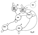
- sequence controller 800 The function of the sequence controller 800 is described in more detail below with reference to FIG. 9 are explained.
- Flow control function block 800 controls the operation of the electronic Ballast, for example, according to the state diagram shown in FIG. 9. 9, each possible operating state is represented by a circle, while the individual arrows represent possible changes of state, which under Fulfillment of a condition associated with the two operating states occur. These conditions are specific to certain states or to certain states Monitoring quantities of the electronic ballast or the lamp (s) linked, these monitoring variables internally in the form of the sequence control 800 are processed by variables which depend on whether the monitoring variable is the appropriate state or not, for example the value "1" when ingested of the assigned state or "0" if the state is not taken.
- the Individual variables monitored by the sequence controller 800 can, for example include time-based variables or error variables.
- the expiry of a commissioning time, a Preheat time, an ignition time or a delay time for the Rectification effect detection can be monitored.
- the error sizes can for example the occurrence of a capacitive current in the load circuit (via the Current detection block 100), the presence of an overvoltage on the connected Gas discharge lamp, the occurrence of a rectification effect or one unbalanced lamp operation, the absence of a lamp or that Occurrence of a synchronization error regarding the zero crossing of the Lamp voltage (each via the voltage detection block 200) are monitored.
- the output signal of the function block 300 can be monitored with whose help is differentiated between a warm and a cold start operation can.
- any other monitoring parameters of the electronic ballast conceivable.
- the individual error quantities are affected by the blocks 100-300 shown in FIG. 3, but first one takes place Processing by the measurement phase control function block 900 before the individual Error quantities are actually evaluated by the sequence control 800.
- To this Purpose contains the measurement phase control for each monitored error size digital event filter assigned to the corresponding error size.
- This digital In principle, event filters perform the function of a counter, which is the continuous occurrence of the corresponding error counts. An error message will appear only then from the corresponding event filter to the sequencer 800 passed on if the corresponding error has occurred n times in succession, where n corresponds to the filter depth of the corresponding digital event filter and for each Error size can be different.
- a filter depth of 64 for the detection of a capacitive current a filter depth of 64, for the detection of an overvoltage a filter depth of 3 and for the detection of a synchronization error as well as for the lamp change detection a filter depth of 7 each can be provided.
- Filter depth values there are others too Filter depth values conceivable.
- the initial state of the operating state control shown in FIG. 9 is the so-called. Reset state (state I).
- the system is in state I whenever the electronic ballast has been started or restarted what synonymous with the occurrence of the enable signal EN explained with reference to FIG. 8 is.
- the sequencer 800 may have a hysteresis Comparator include the external supply voltage signal VCC inside certain limits are monitored and the enable signal EN is generated, if that Supply voltage signal VC within the required Supply voltage range is.
- the comparator monitors in this way at the same time switching the entire system on and off.
- the enable signal EN can thus asynchronous to all depending on switching the entire system on and off other signals occur, whereby after the release signal EN, i.e.
- the sequence control 800 automatically goes into operation a commissioning state (state II).
- state II a commissioning state
- the transition from state I to state II is exceptionally not linked to certain conditions and is done automatically each time the electronic ballast is restarted or restarted.
- state II the harmonic filter starts up or the load circuit of the electronic ballast.
- the coupling capacitor is in state II of the load circuit preloaded. In this phase, all error detectors are deactivated, i.e. there is no evaluation of the error sizes mentioned above.
- a preheating condition III is started from condition II, e.g. a State II assigned commissioning time, which is the normal operating time of the State II denotes, has expired and from the functional block shown in Fig. 3 300 no cold start operation has been reported. However, the commissioning time is still not expired, the system remains in state II, which is shown in FIG. 9 one starting from state II and returning to state II Arrow is shown.
- a cold start operation detected by function block 300 and if the commissioning time has already expired the sequence control 800 changes directly from state II to an ignition state IV, which was explained above Warm start operation corresponds.
- the inverter half bridge is activated in such a way that that it vibrates at the upper limit in frequency and, for example, a Output frequency of approximately 80 kHz is generated.
- the preheating control, overvoltage detection and capacitive current detection must be activated.
- the operating frequency of the electronic inverter Ballast depending on the value of the lamp current detected and the States of overvoltage and capacitive current detection can be changed.
- the control variable "lamp current" First reduce the output frequency of the inverter, since the detected Lamp current because of the not yet ignited compared to the given Setpoint is clearly too small.
- This control process continues until the Overvoltage detection or capacitive current detection the continuous reduction of the Inverter frequency prevented or counteracts this.
- Overvoltage detection should first become dominant as an influencing factor. As a result of The dominance of overvoltage detection that now exists is now, as it were Lamp voltage regulated.
- the ignition state IV can be in the direction of the previously mentioned operating state V only be exited after the specified ignition time. This change of state is in particular regardless of whether in ignition state IV is still related to the ignition voltage or is already regulated based on the lamp current.
- the output frequency of the inverter depends on the lamp current detected.
- This operating state V is the overvoltage, capacitive current and Synchronization error detection activated, even during this state Control circuit only every other period of the inverter output frequency carries out a new setpoint / actual value comparison.
- the rectification effect detection can likewise (GLRE) must be activated.
- the operating state V is not limited in time, i.e. represents in Principle is an endless loop, and can only be activated if one of the activated error detectors are exited.
- all error detectors of the control circuit activated.
- the fault state VII shown in FIG. 9 has started.
- This error condition is VII thus the central point of contact for all serious operational disruptions.
- the Fault state VII is jumped directly from preheating state III, if overvoltage or capacitive current operation during these preheat conditions has been recorded.
- the fault condition VII is based on the Operating state V started if capacitive current operation during this state, an overvoltage error, a synchronization error and / or the occurrence of a Rectification effect, etc. detected with respect to the connected gas discharge lamps has been.
- fault state VII can, for example, occur simultaneously with a appropriate signaling of the respective error for the user.
- Error state VII is only exited by the sequential control system if after a Restart the system again via reset state I, commissioning state II started and the gas discharge lamps are put into operation again.
- the fault state VII can be left if it is detected in this state is that not all lamps connected to the electronic ballast have intact lamp filaments. This is equivalent to the fact that the Fault condition VII in the direction of that already mentioned Lamp change detection status VIII is exited as soon as one of the connected gas discharge lamps is removed from their socket.
- the Operating current consumption of the control circuit reduced to a minimum possible value is.
- the electronic ballast as in Lamp change detection state operated, d. H. it will be the bottom one Inverter switch T3 opened with a low frequency of, for example, 40 Hz and closed while the upper inverter switch is permanently open.
- the control circuit IC2 waits in Fault condition VII on the occurrence of the voltage characteristic curves a or b (see FIG. 7a) on Voltage measurement connection VL1, which is the removal of one of the connected Corresponds to gas discharge lamps G1, G2. In this case, the control circuit IC2 goes in the lamp change detection state VIII.
- the Control circuit both a change or a removal of the top Gas discharge lamp G1 and the lower gas discharge lamp G2 (see FIG. 1) Detect reliably and automatically recognize one after detecting a lamp change Restart the system. While it is checked in error state VII whether a of the gas discharge lamps has been removed in the Lamp change detection status VIII monitors whether all gas discharge lamps are used. Once it has been recognized that all gas discharge lamps are used have been, i.e. all connected to the electronic ballast Lamp filaments are intact, will automatically return to commissioning state II switched and the gas discharge lamps again according to that shown in Fig. 9 Functional circuit put into operation. Even during the Lamp change detection status VIII are with the exception of Lamp change detection deactivated all other fault detectors.
- the inverter control function block 1000 is used to generate Control signals for the upper and lower inverter switches T2, T3 (see Fig. 1), which are output via the output connections OUTH or OUTL of the control circuit become. Depending on these control signals, the two inverter switches either turned on or open. As a rule, the inverter control generates 1000 alternating control pulses for the control connections OUTH or OUTL of the two inverter switches T2 and T3 and can also have an internal Have dead time counter function to ensure a sufficient dead time between the control of the two inverter switches. In the lamp change detection state VIII (see FIG.
- the inverter control 1000 ensures that the upper Output connection OUTH the upper inverter switch T2 remains permanently open, while only the lower inverter switch T3 with a relatively low Frequency alternately opened via the lower output connection OUTL and is closed.
- the inverter control 1000 ensures in particular an asymmetrical Duty cycle of the inverter switch, however, this asymmetry with a Output frequency of the inverter of, for example, 43 kHz only 2.1% and at an output frequency of 80kHz is only 4% and therefore hardly significant falls.
- the generation of unbalanced output signals for the two Inverter switch leads to an increase in the frequency resolution of the Inverter, i.e. with the help of the control circuit, smaller frequency steps of the Inverter can be set.
Claims (7)
- Ballast électronique pour le fonctionnement d'au moins une lampe à décharge, équipé d'une source de tension alternative (D), d'un circuit de charge (E) commandé par la source de tension alternative (D), qui contient au moins une lampe à décharge (G1, G2), et d'un circuit de commande (IC2) en vue de la commande du fonctionnement de la lampe à décharge (G1, G2), qui surveille une grandeur de commutation du ballast électronique et en fonction de la valeur de cette grandeur de commutation lors du déclenchement du ballast électronique actionne la lampe à décharge (G1, G2), soit avec un préchauffage du filament de la lampe à décharge (G1, G2), soit sans préchauffage, le circuit de commande (IC2) contrôle en tant que grandeur de commutation contrôlée du ballast électronique un potentiel de tension appliqué au circuit de commande (IC2) et correspondant à l'état de charge d'un circuit accumulateur d'énergie (R22, C17), le circuit accumulateur d'énergie (R22, C17) étant chargé durant le fonctionnement de la lampe à décharge (G1, G2) à un potentiel de tension d'alimentation prescrit (VDD) et se déchargeant lors de la coupure du ballast électronique selon une constante de temps déterminée, le circuit de commande (IC2) comprenant un moyen de comparaison (301) en vue de la comparaison du potentiel de tension appliqué au circuit de commande (IC2) à une valeur de référence (Vref12), et le circuit de commande (IC2) actionnant la lampe à décharge sans préchauffage, au cas où le moyen de comparaison (301) indique un potentiel de tension appliqué au circuit de commande (IC2), qui est supérieur à la valeur de référence (Vref12), et dans l'autre cas, actionne la lampe à décharge (G1, G2) avec préchauffage,
caractérisé en ce que le signal de sortie du moyen comparateur (301) est appliqué à un circuit de maintien d'état (302), qui délivre le signal de sortie du moyen comparateur (301) uniquement lors du démarrage du ballast électronique, le circuit de commande (IC2) évaluant le signal de sortie du circuit de maintien d'état (302) pour la mise en marche de la lampe à décharge (G1, G2) sélectivement avec ou sans préchauffage. - Ballast électronique selon la revendication 1, caractérisé en ce que la tension de référence appliquée au moyen comparateur (301) s'élève à environ 1V.
- Ballast électronique selon la revendication 1 ou 2, caractérisé en ce que le circuit de maintien d'état (302) comprend une bascule-D, à l'entrée d'horloge de laquelle est appliqué un signal d'horloge, qui présente temporairement un niveau haut uniquement lors du démarrage du ballast électronique.
- Ballast électronique selon une des revendications précédentes, caractérisé en ce que le circuit accumulateur d'énergie comprend un circuit série avec un condensateur de charge (C17) et une résistance (R22) relié à une borne (NP) du circuit de commande (IC2).
- Ballast électronique selon l'une des revendications précédentes, caractérisé en ce que le circuit accumulateur d'énergie (R22, C17) présente une constante de temps, en ce le potentiel de tension contrôlé par le circuit de commande (IC2) et fonction de l'état de charge du circuit accumulateur d'énergie est supérieur après coupure du ballast électronique pendant une durée d'environ 400 ms supérieur à la valeur de référence (Vref12) appliquée au circuit de commande (IC2).
- Ballast électronique selon l'une des revendications précédentes, caractérisé en ce que le circuit accumulateur d'énergie (R22, C17) est relié par l'intermédiaire d'un commutateur commandé (301) à une source de tension d'alimentation (VDD), le circuit accumulateur d'énergie (R22, C17) étant chargé par fermeture du commutateur commandé (S301).
- Ballast électronique selon la revendication 6, caractérisé en ce que le circuit de commande (IC2) command le commutateur commandé (S301) de telle sorte que celui-ci est tout d'abord ouvert lors du démarrage du ballast électronique et est fermé après l'amorçage de la lampe à décharge (G1, G2) et est à nouveau ouvert lors de la coupure du ballast électronique.
Applications Claiming Priority (3)
| Application Number | Priority Date | Filing Date | Title |
|---|---|---|---|
| DE19757667 | 1997-12-23 | ||
| DE19757667 | 1997-12-23 | ||
| PCT/EP1998/007426 WO1999034648A1 (de) | 1997-12-23 | 1998-11-19 | Elektronisches vorschaltgerät |
Publications (2)
| Publication Number | Publication Date |
|---|---|
| EP1048190A1 EP1048190A1 (fr) | 2000-11-02 |
| EP1048190B1 true EP1048190B1 (fr) | 2003-05-07 |
Family
ID=7853257
Family Applications (1)
| Application Number | Title | Priority Date | Filing Date |
|---|---|---|---|
| EP98964410A Expired - Lifetime EP1048190B1 (fr) | 1997-12-23 | 1998-11-19 | Ballast electronique pour lampe a decharge |
Country Status (7)
| Country | Link |
|---|---|
| EP (1) | EP1048190B1 (fr) |
| AT (1) | ATE240030T1 (fr) |
| AU (1) | AU1962499A (fr) |
| DE (1) | DE59808310D1 (fr) |
| ES (1) | ES2195438T3 (fr) |
| WO (1) | WO1999034648A1 (fr) |
| ZA (1) | ZA9811774B (fr) |
Families Citing this family (3)
| Publication number | Priority date | Publication date | Assignee | Title |
|---|---|---|---|---|
| DE10134566A1 (de) * | 2001-07-16 | 2003-02-06 | Tridonicatco Gmbh & Co Kg | Elektronisches Vorschaltgerät mit Vorheizbetrieb |
| DE10206731B4 (de) * | 2002-02-18 | 2016-12-22 | Tridonic Gmbh & Co Kg | Lampensensor für ein Vorschaltgerät zum Betrieb einer Gasentladunslampe |
| DE102005042527B4 (de) * | 2005-09-07 | 2015-10-29 | Osram Gmbh | Schaltungsanordnung und Verfahren zum Betreiben einer Entladungslampe |
Family Cites Families (6)
| Publication number | Priority date | Publication date | Assignee | Title |
|---|---|---|---|---|
| IT1121148B (it) * | 1979-06-26 | 1986-03-26 | Siliani Pier | Circuito d accensione per tubi fluorescenti e simili con riscaldamento preliminare dei filamenti |
| US4958108A (en) * | 1989-02-14 | 1990-09-18 | Avtech Corporation | Universal fluorescent lamp ballast |
| US5030887A (en) * | 1990-01-29 | 1991-07-09 | Guisinger John E | High frequency fluorescent lamp exciter |
| DE59209173D1 (de) * | 1992-10-28 | 1998-03-05 | Knobel Lichttech | Verfahren und Schaltungsanordnung zum Zünden von Leuchtstofflampen bei vorbestimmter Temperatur der Lampenkathoden |
| NL9301694A (nl) * | 1993-10-01 | 1995-05-01 | Cm Personnel Participation Bv | Electronische voorschakelinrichting voor gasontladingsbuizen. |
| US5424611A (en) * | 1993-12-22 | 1995-06-13 | At&T Corp. | Method for pre-heating a gas-discharge lamp |
-
1998
- 1998-11-19 EP EP98964410A patent/EP1048190B1/fr not_active Expired - Lifetime
- 1998-11-19 ES ES98964410T patent/ES2195438T3/es not_active Expired - Lifetime
- 1998-11-19 WO PCT/EP1998/007426 patent/WO1999034648A1/de active IP Right Grant
- 1998-11-19 AU AU19624/99A patent/AU1962499A/en not_active Abandoned
- 1998-11-19 AT AT98964410T patent/ATE240030T1/de active
- 1998-11-19 DE DE59808310T patent/DE59808310D1/de not_active Expired - Lifetime
- 1998-12-22 ZA ZA9811774A patent/ZA9811774B/xx unknown
Also Published As
| Publication number | Publication date |
|---|---|
| ATE240030T1 (de) | 2003-05-15 |
| WO1999034648A1 (de) | 1999-07-08 |
| EP1048190A1 (fr) | 2000-11-02 |
| DE59808310D1 (de) | 2003-06-12 |
| ZA9811774B (en) | 1999-06-29 |
| AU1962499A (en) | 1999-07-19 |
| ES2195438T3 (es) | 2003-12-01 |
Similar Documents
| Publication | Publication Date | Title |
|---|---|---|
| EP1066739B1 (fr) | Procede et dispositif permettant de detecter l'effet redresseur apparaissant dans une lampe a decharge | |
| EP1103165B1 (fr) | Ballast electronique destine a au moins une lampe a decharge basse tension | |
| EP1519638B1 (fr) | Méthode pour commander une lampe à décharge basse pression | |
| DE69628739T2 (de) | Steuerung und überwachung von dimmbaren vorschaltgeräten mit breitem beleuchtungshub | |
| EP0708579A1 (fr) | Procédé et appareil pour alimenter une lampe à décharge | |
| EP0801881A1 (fr) | Procede permettant de faire fonctionner au moins une lampe a fluorescence au moyen d'un ballast electronique et ballast electronique utilise a cet effet | |
| EP0965249A1 (fr) | Procede et dispositif de detection de l'effet de redressement dans une lampe a decharge | |
| EP1103166B1 (fr) | Ballast electronique destine a au moins une lampe a decharge basse tension | |
| DE4406083A1 (de) | Schaltungsanordnung zum Betrieb mindestens einer Niederdruckentladungslampe | |
| AT517946B1 (de) | Verfahren, betriebsgerät und beleuchtungssystem | |
| DE102004037388B4 (de) | Verfahren zur Detektion eines Nicht-Nullspannungsschaltbetriebs eines Vorschaltgeräts für Leuchtstofflampen und Vorschaltgerät | |
| EP1425943B1 (fr) | Procede et dispositif destines au fonctionnement economique d'un tube fluorescent | |
| EP1040733B1 (fr) | Ballast electronique | |
| EP1901591B1 (fr) | Allumage de lampes à décharge dans des conditions environnementales variables | |
| DE19916878B4 (de) | Schaltungsanordnung und Verfahren zum Betreiben von Gasentladungslampen | |
| EP1048190B1 (fr) | Ballast electronique pour lampe a decharge | |
| EP1040732B1 (fr) | Procede de detection de changement de lampe et ballast electronique destine au fonctionnement de lampes a decharge a l'aide d'un tel procede de detection de changement de lampe | |
| DE102004037389B4 (de) | Verfahren zur Ansteuerung einer eine Leuchtstofflampe aufweisenden Last zur Optimierung des Zündvorganges | |
| EP1280388B1 (fr) | Ballast électronique avec un mode de préchauffage | |
| EP2796012B1 (fr) | Procédé, appareillage d'alimentation et système d'éclairage, avec détection d'effet de redressement de lampes | |
| DE102010040449A1 (de) | Schaltungsanordnung und Verfahren zum Starten und Betreiben einer Hochdruckentladungslampe | |
| DE102004025774A1 (de) | Vorschaltgerät für Entladungslampe mit Dauerbetriebs-Regelschaltung | |
| DE19934687A1 (de) | Elektronisches Vorschaltgerät für mindestens eine Niederdruck-Entladungslampe | |
| DE10007784A1 (de) | Schaltungsanordnung für eine Leuchtstofflampe | |
| DE102009053617A1 (de) | Elektronisches Vorschaltgerät und Verfahren zum Betreiben mindestens einer Entladungslampe |
Legal Events
| Date | Code | Title | Description |
|---|---|---|---|
| PUAI | Public reference made under article 153(3) epc to a published international application that has entered the european phase |
Free format text: ORIGINAL CODE: 0009012 |
|
| 17P | Request for examination filed |
Effective date: 20000412 |
|
| AK | Designated contracting states |
Kind code of ref document: A1 Designated state(s): AT CH DE ES FI FR GB IT LI NL SE |
|
| 17Q | First examination report despatched |
Effective date: 20010412 |
|
| RAP1 | Party data changed (applicant data changed or rights of an application transferred) |
Owner name: TRIDONICATCO GMBH & CO. KG |
|
| GRAH | Despatch of communication of intention to grant a patent |
Free format text: ORIGINAL CODE: EPIDOS IGRA |
|
| GRAH | Despatch of communication of intention to grant a patent |
Free format text: ORIGINAL CODE: EPIDOS IGRA |
|
| GRAA | (expected) grant |
Free format text: ORIGINAL CODE: 0009210 |
|
| AK | Designated contracting states |
Designated state(s): AT CH DE ES FI FR GB IT LI NL SE |
|
| REG | Reference to a national code |
Ref country code: GB Ref legal event code: FG4D Free format text: NOT ENGLISH |
|
| RIC1 | Information provided on ipc code assigned before grant |
Ipc: 7H 05B 41/298 A |
|
| REG | Reference to a national code |
Ref country code: CH Ref legal event code: EP |
|
| REG | Reference to a national code |
Ref country code: CH Ref legal event code: NV Representative=s name: A. BRAUN, BRAUN, HERITIER, ESCHMANN AG PATENTANWAE |
|
| REF | Corresponds to: |
Ref document number: 59808310 Country of ref document: DE Date of ref document: 20030612 Kind code of ref document: P |
|
| REG | Reference to a national code |
Ref country code: SE Ref legal event code: TRGR |
|
| GBT | Gb: translation of ep patent filed (gb section 77(6)(a)/1977) | ||
| NLR4 | Nl: receipt of corrected translation in the netherlands language at the initiative of the proprietor of the patent | ||
| ET | Fr: translation filed | ||
| PLBE | No opposition filed within time limit |
Free format text: ORIGINAL CODE: 0009261 |
|
| STAA | Information on the status of an ep patent application or granted ep patent |
Free format text: STATUS: NO OPPOSITION FILED WITHIN TIME LIMIT |
|
| 26N | No opposition filed |
Effective date: 20040210 |
|
| REG | Reference to a national code |
Ref country code: CH Ref legal event code: PFA Owner name: TRIDONICATCO GMBH & CO. KG Free format text: TRIDONICATCO GMBH & CO. KG#FAERBERGASSE 15#6851 DORNBIRN (AT) -TRANSFER TO- TRIDONICATCO GMBH & CO. KG#FAERBERGASSE 15#6851 DORNBIRN (AT) |
|
| PGFP | Annual fee paid to national office [announced via postgrant information from national office to epo] |
Ref country code: NL Payment date: 20081120 Year of fee payment: 11 |
|
| REG | Reference to a national code |
Ref country code: NL Ref legal event code: V1 Effective date: 20100601 |
|
| PG25 | Lapsed in a contracting state [announced via postgrant information from national office to epo] |
Ref country code: NL Free format text: LAPSE BECAUSE OF NON-PAYMENT OF DUE FEES Effective date: 20100601 |
|
| PGFP | Annual fee paid to national office [announced via postgrant information from national office to epo] |
Ref country code: CH Payment date: 20111130 Year of fee payment: 14 |
|
| PGFP | Annual fee paid to national office [announced via postgrant information from national office to epo] |
Ref country code: FI Payment date: 20121126 Year of fee payment: 15 |
|
| PGFP | Annual fee paid to national office [announced via postgrant information from national office to epo] |
Ref country code: ES Payment date: 20121217 Year of fee payment: 15 Ref country code: SE Payment date: 20121128 Year of fee payment: 15 |
|
| REG | Reference to a national code |
Ref country code: CH Ref legal event code: PL |
|
| PG25 | Lapsed in a contracting state [announced via postgrant information from national office to epo] |
Ref country code: CH Free format text: LAPSE BECAUSE OF NON-PAYMENT OF DUE FEES Effective date: 20121130 Ref country code: LI Free format text: LAPSE BECAUSE OF NON-PAYMENT OF DUE FEES Effective date: 20121130 |
|
| PGFP | Annual fee paid to national office [announced via postgrant information from national office to epo] |
Ref country code: AT Payment date: 20131128 Year of fee payment: 16 |
|
| PGFP | Annual fee paid to national office [announced via postgrant information from national office to epo] |
Ref country code: IT Payment date: 20131127 Year of fee payment: 16 |
|
| REG | Reference to a national code |
Ref country code: SE Ref legal event code: EUG |
|
| PG25 | Lapsed in a contracting state [announced via postgrant information from national office to epo] |
Ref country code: SE Free format text: LAPSE BECAUSE OF NON-PAYMENT OF DUE FEES Effective date: 20131120 Ref country code: FI Free format text: LAPSE BECAUSE OF NON-PAYMENT OF DUE FEES Effective date: 20131119 |
|
| PGFP | Annual fee paid to national office [announced via postgrant information from national office to epo] |
Ref country code: GB Payment date: 20141128 Year of fee payment: 17 |
|
| PGFP | Annual fee paid to national office [announced via postgrant information from national office to epo] |
Ref country code: FR Payment date: 20141126 Year of fee payment: 17 |
|
| REG | Reference to a national code |
Ref country code: ES Ref legal event code: FD2A Effective date: 20150408 |
|
| PG25 | Lapsed in a contracting state [announced via postgrant information from national office to epo] |
Ref country code: ES Free format text: LAPSE BECAUSE OF NON-PAYMENT OF DUE FEES Effective date: 20131120 |
|
| PGFP | Annual fee paid to national office [announced via postgrant information from national office to epo] |
Ref country code: DE Payment date: 20150129 Year of fee payment: 17 |
|
| REG | Reference to a national code |
Ref country code: AT Ref legal event code: MM01 Ref document number: 240030 Country of ref document: AT Kind code of ref document: T Effective date: 20141119 |
|
| PG25 | Lapsed in a contracting state [announced via postgrant information from national office to epo] |
Ref country code: AT Free format text: LAPSE BECAUSE OF NON-PAYMENT OF DUE FEES Effective date: 20141119 |
|
| PG25 | Lapsed in a contracting state [announced via postgrant information from national office to epo] |
Ref country code: IT Free format text: LAPSE BECAUSE OF NON-PAYMENT OF DUE FEES Effective date: 20141119 |
|
| REG | Reference to a national code |
Ref country code: DE Ref legal event code: R119 Ref document number: 59808310 Country of ref document: DE |
|
| GBPC | Gb: european patent ceased through non-payment of renewal fee |
Effective date: 20151119 |
|
| REG | Reference to a national code |
Ref country code: FR Ref legal event code: ST Effective date: 20160729 |
|
| PG25 | Lapsed in a contracting state [announced via postgrant information from national office to epo] |
Ref country code: DE Free format text: LAPSE BECAUSE OF NON-PAYMENT OF DUE FEES Effective date: 20160601 Ref country code: GB Free format text: LAPSE BECAUSE OF NON-PAYMENT OF DUE FEES Effective date: 20151119 |
|
| PG25 | Lapsed in a contracting state [announced via postgrant information from national office to epo] |
Ref country code: FR Free format text: LAPSE BECAUSE OF NON-PAYMENT OF DUE FEES Effective date: 20151130 |