EP1045558B1 - Zeitmultiplex-Vermittlungssystem (TDM) mit sehr breitem Speicher - Google Patents
Zeitmultiplex-Vermittlungssystem (TDM) mit sehr breitem Speicher Download PDFInfo
- Publication number
- EP1045558B1 EP1045558B1 EP00302910A EP00302910A EP1045558B1 EP 1045558 B1 EP1045558 B1 EP 1045558B1 EP 00302910 A EP00302910 A EP 00302910A EP 00302910 A EP00302910 A EP 00302910A EP 1045558 B1 EP1045558 B1 EP 1045558B1
- Authority
- EP
- European Patent Office
- Prior art keywords
- packets
- width
- memory
- bus
- packet
- Prior art date
- Legal status (The legal status is an assumption and is not a legal conclusion. Google has not performed a legal analysis and makes no representation as to the accuracy of the status listed.)
- Expired - Lifetime
Links
Images


Classifications
-
- H—ELECTRICITY
- H04—ELECTRIC COMMUNICATION TECHNIQUE
- H04Q—SELECTING
- H04Q11/00—Selecting arrangements for multiplex systems
- H04Q11/04—Selecting arrangements for multiplex systems for time-division multiplexing
-
- H—ELECTRICITY
- H04—ELECTRIC COMMUNICATION TECHNIQUE
- H04Q—SELECTING
- H04Q2213/00—Indexing scheme relating to selecting arrangements in general and for multiplex systems
- H04Q2213/13103—Memory
-
- H—ELECTRICITY
- H04—ELECTRIC COMMUNICATION TECHNIQUE
- H04Q—SELECTING
- H04Q2213/00—Indexing scheme relating to selecting arrangements in general and for multiplex systems
- H04Q2213/13292—Time division multiplexing, TDM
-
- H—ELECTRICITY
- H04—ELECTRIC COMMUNICATION TECHNIQUE
- H04Q—SELECTING
- H04Q2213/00—Indexing scheme relating to selecting arrangements in general and for multiplex systems
- H04Q2213/13299—Bus
Definitions
- the present invention is related to time division multiplexed switches. More specifically, the present invention relates to time division multiplexing of switches where a memory bus width is independent of the width of any packet.
- Time division multiplexing is one technique used to implement a switching system.
- a switch fabric with N input ports that each receive packets at rate R and N output ports that each transmit packets at rate R, as shown in figure 1.
- N input ports that each receive packets at rate R
- N output ports that each transmit packets at rate R
- FIG 1 For a shared memory TDM switching system, a single memory bus is required that has an aggregate bandwidth of 2xNxR.
- the arriving packets are aggregated and written to the memory. Once written to memory, the packets are read out of the memory and transmitted on the output ports.
- Memory bandwidth can be increased by increasing the speed and width of the memory bus.
- Current memory bus speeds are technology limited to roughly 300MHz, using microprocessor synchronous cache memories. To further increase memory bandwidth, the memory bus must be made wider.
- each input port is allocated one clock cycle to write a packet (8-bits) to memory and each output port is allocated one clock cycle to read a packet from memory.
- TDM switching systems There are several issues that complicate the design of TDM switching systems in practice. Depending on the application of the switching system, packets usually vary in size. Variable sized packets reduce the performance of TDM systems due to packet fragmentation on the memory bus. If a packet doesn't utilize an integral number of memory cycles, memory bandwidth is wasted on memory cycles that read or write data that is less than the memory bus width. Typically, TDM systems are implemented with a memory bandwidth greater than 2xNxR to compensate for inefficiencies due to fragmentation.
- Fragmentation issues become significant as the memory width approaches, or exceeds, the minimum sized data packet.
- a memory bus width that is equal to twice the minimum packet length.
- the memory system bandwidth is reduced by 50% (or is 50% efficient), since all packets written to memory utilize only half of the memory bus data bits.
- TDM switching systems Due to packet fragmentation on the memory bus, typical TDM switching systems utilize bus widths that are at most as wide as a minimum length packet.
- the total bandwidth of a shared memory TDM switching system is limited by the bandwidth of the memory bus.
- Memory bus bandwidth is determined by its speed (clock rate) and its width (number of bits). Given that memory speeds are fixed by the technology of available memory components, then the total bandwidth of TDM switches is limited by the minimum packet size.
- a paper entitled “Fast Switched Backplane for a gigabit switched router” by McKeown (DEPARTMENT OF ELECTRICAL ENGINEERING, STANFORD UNIVERSITY, December 1997 (1997-12), pages 1-30) teaches a fast switched backplane for a gigabit switched router, and focuses on the switched back plane developed for the Cisco 12,000 G S R.
- This router has a high-performance switched backplane architecture capable of switching 16 ports simultaneously, each with a line rate of 2.4Gb/s.
- the backplane has a parallel, compact design providing extremely high throughput for both unicast and multicast traffic.
- a paper entitled “Review of recent shared memory based ATM switches” by Sharma N. K. discloses a NxN cells shared memory type switch incorporating a time-division-multiplex bus, wherein, in each time slot, up to N cells from input ports can be written into the shared memory and up to N cells can be read out of the shared memory.
- US 5,301,192 relates to a temporary information storage system comprising a buffer memory storing data structured in fixed or variable length data blocks.
- the present invention pertains to a switching system.
- the system comprises I input port mechanisms which receive packets having a width from a communication line, where I is greater than or equal to 1 and is an integer.
- the system comprises O output port mechanisms which send packets to a communication line, where O is greater than or equal to 1 and is an integer.
- the system comprises a carrier mechanism along which packets travel. The carrier mechanism has a width wider than the width of the packets.
- the carrier mechanism is connected to each input port mechanism and each output port mechanism.
- the system comprises a memory mechanism in which packets are stored.
- the memory mechanism is connected to the carrier mechanism.
- the system comprises a mechanism for providing packets to the memory mechanism through the carrier mechanism from the input port mechanisms.
- the providing mechanism is able to transfer packets or portions of packets whose total width equals the width of the carrier mechanism in each transfer cycle to the memory mechanism.
- the providing mechanism includes input queue groups connected to the carrier mechanism and the input port mechanisms for storing packets received by the input port mechanisms, and output queue groups connected to the providing mechanism and the output port mechanisms for storing packets to be sent out the output port mechanisms with each queue group corresponding to a packet.
- the present invention pertains to a method for switching packets from input mechanisms to output mechanisms, each having a width.
- the method comprises the steps of receiving a first packet and at least a second packet at a switch mechanism.
- the method comprises the steps of transferring data of the first packet and the second packets to a memory mechanism via time division multiplexing of a bus having a width which is a positive non-integer multiple of the packet width so data from the packets fills a predetermined portion of the width of the bus by placing the first packet and at least the second packet in an input queue group, and transferring data in the input queue group during an allocated time slot on the bus to the memory mechanism so the data fills the predetermined portion of the width of the bus.
- the system 10 comprises I input port mechanisms 12 having a width which receive packets from a communication line 16, where I is greater than or equal to 1 and is an integer.
- an input port mechanism 12 includes an input port.
- the system 10 comprises O output port mechanisms 14 having a width which send packets to a communication line 16, where O is greater than or equal to 1 and is an integer.
- an output port mechanism 14 includes an output port.
- the system 10 comprises a carrier mechanism 18 along which packets travel. The carrier mechanism 18 has a width wider than the width of the input and output mechanisms.
- the carrier mechanism 18 is connected to each input port mechanism and each output port mechanism.
- the system 10 comprises a memory mechanism 22 in which packets are stored.
- the memory mechanism 22 is connected to the carrier mechanism 18.
- the system 10 comprises a mechanism for providing packets to the memory mechanism 22 though the carrier mechanism 18 from the input port mechanisms 12.
- the providing mechanism 20 is able to transfer packets or portions of packets whose total size equals the width of the carrier mechanism 20 in each transfer cycle to the memory mechanism 22.
- the width of the carrier mechanism 18 is independent of the width of any of the input and output mechanisms.
- the input port mechanism preferably receives variable sized packets.
- the output port mechanism sends variable sized packets to the communication line 16.
- the communication line 16 can be an ATM network.
- the providing mechanism 20 also provides packets from the memory mechanism 22 to the output port mechanisms 14 through the carrier mechanism 18.
- the providing mechanism 20 is able to transfer packets or portions of packets whose total size equals the width of the carrier mechanism 18 in each transfer cycle from the memory mechanism 22.
- the providing mechanism 20 preferably includes an input stage of queue groups 24 connected to the carrier mechanism 20 and the input port mechanisms 12 for storing packets received by the input port mechanisms 12, and an output stage of queue groups 26 connected to the providing mechanism 20 and the output port mechanisms 14 for storing packets to be sent out the output port mechanisms 14, with each queue group corresponding to a packet.
- the providing mechanism 20 includes a classifying mechanism 28 which places a packet which is received by the input port mechanism into a corresponding input stage queue group, said classifying mechanism 28 connected to the input port mechanisms 12 and the input queue groups 24.
- the providing mechanism 20 preferably includes a processing mechanism 30 which places a packet in an output stage queue group into a corresponding output port mechanism, said processing mechanism 30 connected to the output port mechanisms 14 and the output stage queue groups 26.
- the classifying mechanism 28 includes a first write finite state machine 32 for writing packets into a corresponding input queue
- the providing mechanism 20 includes a second write finite state machine 34 for writing packets from an input stage queue group into the memory mechanism 22, and a first read finite state machine 36 for reading packets from the memory mechanism 22 to an output stage queue group
- mechanism 30 includes a second read finite state machine 38 for reading a packet from the output stage queue group to the network.
- the memory mechanism 22 preferably includes a shared memory 40.
- packets or portions of packets travel on the carrier mechanism 18 based on time division multiplexing.
- the carrier mechanism 18 preferably includes a bus 42.
- the first read finite state machine 36 only transfers data of packets of an input stage queue group to the bus 42 when the input stage queue group contains at least one cache-line of data.
- the present invention pertains to a switching system 10 for packets.
- the system 10 comprises a central resource 44 having a width and an overall bandwidth and input port mechanisms 12 and output port mechanisms 14 for receiving or sending packets, respectively.
- the central resource 44 is partitioned via time slots that are allocated to the input and output port mechanisms 12 and 14.
- the central resource 44 width is independent of any input port or output port mechanisms width and the overall bandwidth can grow without bound.
- the system 10 comprises a memory mechanism 22 for storing packets.
- the memory mechanism 22 is connected to the central resource 44.
- the central resource 44 includes a memory bus 42.
- the central resource 44 preferably includes queue groups in which packets are classified, and the packets are read from and written into the memory mechanism 22 from the queue groups.
- the present invention pertains to a switching system 10.
- the system 10 comprises a time division multiplex bus 42.
- the system 10 comprises a memory mechanism 22 connected to the bus 42 which is accessed via time division multiplexing of the bus 42.
- the system 10 comprises a mechanism for reading and writing data of packets to the memory mechanism 22 through the bus 42 without knowledge of the packet boundaries of the data.
- the present invention pertains to a switching system 10.
- the system 10 comprises a time division multiplex carrier mechanism 20 having a width.
- the system 10 comprises a memory mechanism 22 connected to the carrier mechanism 18.
- the system 10 comprises a mechanism for providing data of packets to the memory mechanism 22 from an input port mechanism having a width so the data of the packets fills the width of the bus 42 via time division multiplexing.
- the system 10 comprises a mechanism for providing data of packets from the memory mechanism 22 to an output port mechanism having a width.
- the bus 42 width is a positive non-integer multiple of the input and output port mechanism widths.
- the present invention pertains to a method for switching packets.
- the method comprises the steps of receiving a first packet and at least a second packet at a switch mechanism having a width.
- the method comprises the steps of transferring data of the first packet and the second packet to a memory mechanism 22 via time division multiplexing of a bus 42 having a width so data from the packets fills a predetermined portion of the width of the bus 42.
- the bus 42 width is not equal to the input port mechanism width.
- the bus 42 width preferably is a positive multiple of the input port mechanism width and can be a non-integer multiple.
- the transferring step includes the steps of placing the first packet and at least the second packet in an input stage queue group; and transferring data in the input stage queue group during an allocated time slot on the bus 42 to the memory mechanism 22 so the data fills the predetermined portion of the width of the bus 42.
- the step of determining that the input stage queue group has at least one-cache line of data is preferably the step of determining that the input stage queue group has at least one-cache line of data.
- the memory width limitation of typical TDM switching systems is removed by classifying packets into input stage queue groups 24 and then reading and writing data from the input stage queue groups 24 to memory.
- the memory width is independent of the minimum packet size and the overall bandwidth of the TDM switching system 10 can grow without bounds.
- the packets that arrive on the input ports of the switching system 10 are classified into a fixed number of queue groups 24.
- a queue is implemented for each group in three stages:
- Reads and writes to shared memory are implemented on data in the queue group and are performed without knowledge of the packet boundaries of the data in the queue. Access to the shared memory is allocated to the Read and Write FSMs via time division multiplexing of the shared memory bus 42.
- the width of the shared memory bus 42 is called a cache-line.
- the W-FSM is implemented as follows:
- a cell or a packet arrives at an input port of the switch 45.
- a first write finite state machine 32 classifies the packet into a queue group 24. As other packets arrive at input ports of the switch 45, they are also classified by the first write finite state machine 32 into their corresponding queue group 24. Once classified into a queue group, they are appended to the end of the corresponding input stage queue group. This classifying and filling of cells received at input ports of the switch 45 continues over time. In regard to a specific input queue group 24, as a packet is categorized and classified to it, the packet is added to the tail of the corresponding input queue group 24.
- a second write finite state machine 34 corresponding with the input stage queue group 24 keeps track of the number of packets in the input stage queue group 24. When there are enough packets in the input stage queue group 24 for the data in the input stage queue group 24 to fill the cache line of the memory 40 bus, the second write finite state machine 34 waits for the input queue group's 24 allocated time slot on the bus to arrive.
- the second write finite state machine 34 sends enough data from the input stage queue group 24 to fill a cache-line on the bus during the allocated slot of the input queue group 24.
- the allocated slot is of long enough duration to allow a cache-line of data to be sent onto the bus from the input stage queue group 24. As the cache line of data from the input stage queue group 24 is sent on the bus, the data that remains in the input stage queue group 24 is moved up to the head of the input stage queue group 24.
- the data that is moved up to the head of the input stage queue group 24 makes room for additional packets and thus data to be placed into the input stage queue group 24. There can be times when data is being sent onto the bus from the input stage queue group 24 and at the same time cells are being placed onto the tail of the input stage queue group 24.
- the data that is sent over the bus can be other than an integer multiple of packets in the input queue group 24 have.
- the cache-line is of a width that a portion of a packet remains in the input stage queue group 24 after the cache-line of data has been sent onto the bus to the memory 40.
- the second write finite state machine 34 is unaware of cell or packet boundaries and is only concerned with filling the cache-line with data whatever the result to the integrity of the cell or packet is. Thus, a cell or packet is broken up to accommodate the constraint that the data fills the cache-line during the allocated slot.
- a controller 47 When the cache-line of data arrives at the shared memory 40 from the bus, a controller 47 stores the cache-line of data in the shared memory 40 and records the address in the shared memory 40 where the cache-line is stored as well as the order of that cache-line from the input stage queue group 24 and the input stage queue group 24 from which the cache-line arrives. Over time, cache-lines of data from different input stage queue groups 24 will be stored in the shared memory 40 by the controller 47, as well as the next cache-line sent by the input stage queue group 24 to the shared memory 40. The controller 47 keeps track of the addresses where the cache-lines from an input stage queue group 24 are stored.
- Subsequent cache-lines from an input stage queue group 24 do not necessarily need to be stored in the same address or even in two addresses next to each other, even though, for instance, the first cache-line from the input stage queue group 24 might have the first part of a cell and the second cache-line from the input stage queue group 24 might have the second part of the cell. This is not necessary as long as the controller 47 knows where the cache-lines from the input stage queue group 24 are located and the order in which the cache-lines arrived at the shared memory 40.
- a first read finite state machine 36 corresponding to an output stage queue group 26 waits for the output stage queue group's 26 allocated time slot on the bus to arrive.
- the first read finite state machine 36 keeps track of data in the shared memory 40 which are to be read into the output stage queue group 26.
- the first read finite state machine 36 is in communication with the controller 47 and the write finite state machines so it knows which data is to go to the output stage queue group 26 to which it corresponds.
- the allocated time slot arrives for the output stage queue group 26
- the cache line whose turn it is next to be read from the shared memory 40 is read by the first read finite state machine 36 to the tail of the output stage queue group 26.
- the cache-line in the shared memory 40 for the output stage queue group 26 is read into the output stage queue group 26 by the first read finite state machine 36.
- the first read finite state machine 36 knows from which address to read a cache-line by communicating with the controller 47. Since cache-lines are read in order, and placed on the tail of the output stage queue group 26, any cells that have been broken up during the writing stage into the shared memory 40 are reunited when the separate cache-lines are reunited in the output stage queue group 26. If there is no data in the shared memory 40 when the allocated time slot for the output stage queue group arrives, then the read finite state machine will read data up to the cache-line directly from an input stage queue group 24 whose data is to ultimately go into the output stage queue group 26.
- a second read finite state machine 38 keeps track of the packets in the output stage queue groups. Only when a predetermined amount of packets, are formed in the output stage queue group 26 will the second read finite state machine 38 read packets up to a predetermined amount from the output stage queue group 26 and send them to an output port which sends them onto the network.
- memory bus 42 efficiency is 100%. Small packets do not cause fragmentation of data on the memory bus 42. Furthermore, the memory bus width can grow without bounds and is not limited by packet size.
- the queue group model can be used to implement arbitrary queuing structures. To implement output queues, one queue group is allocated for each output port. A queue group consists of the input stage queue group, some number of cache-lines stored in the shared memory, and the output stage queue group.
- the packet classifier examines each packet on input, and classifies the packet into the appropriate output queue. The packets are routed to the input stage queue group that corresponds to that output queue.
- the output queues 28 are queued to/from memory using the W-FSMs and R-FSMs. After the R-FSM, the packets are queued immediately to an output port.
- Input queues are implemented using a trivial packet classifier, by associating one queue group 24 for each input port.
- a priority-based scheme can be implemented as follows.
- a queue group is defined for each of several priority levels.
- the queue groups are queued to memory using the W-FSMs and R-FSMs. After the R-FSM, the packets are processed to determine their output ports and transmitted from the fabric.
- a four input port, four output port packet switch is implemented using the system 10.
- the system is globally synchronous and operates on a 20MHz clock.
- the four inputs operate at 8-bits wide and implement four 160 Mbps interfaces.
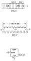
- the packets are delineated using a start of packet (SOP) and end of packet (EOP) code word, as shown in figure 5.
- SOP start of packet
- EOP end of packet
- the example assumes an output queued switch.
- the packets that arrive on the input ports of the switching system 10 are classified into four queue groups, one for each output port. Referring to figure 4, an output queue is implemented for each group in three sub-systems:
- Reads and writes to shared memory are implemented on data in the queue group and are performed without knowledge of the packet boundaries of the data in the queue. Access to the shared memory is allocated to the Read and Write FSMs via time division multiplexing of the shared memory bus.
- the width of the shared memory bus is called a cache-line.
- the head and tail of the queue group located in the input stage and output stage of the invention are implemented directly in shift registers 51.
- the shift registers 51 are as wide as the incoming data interfaces and as long as the memory cacheline.
- the data path for the four port switch is shown in figure 6.
- the cacheline is 64-bits long and contains eight bytes. Data from each port is shifted into an 8-register deep, 8-bit wide cacheline shift register. Not shown is a synchronization shift register prior to the shift register that is also an 8-deep 8-bit register.
- the memory bus is divided in a TDM (time division multiplex) fashion into eight time slots 53, one for each input and output port, as shown in figure 7. Since the example switch implements output queues, the output stage queues are always drained at the same rate, and therefore always use the same time slot on the bus. Since arriving packets can be destined for any output port, the input stage queues can be filled at any arbitrary rate.
- the input stage groups are allocated the input bus time slots as they are needed. Since the total input rate does not exceed four time slots, it is sufficient to let the input stages arbitrate for the four input stage time slots.
- the synchronization register is used to guarantee that no data is lost. Data typically is not stored in the synchronization register. All arriving packets are written directly into the cacheline register. If the cacheline register fills prior to its time slot on the TDM bus, then the synchronization register begins storing data. Once the cacheline register is emptied, the data from the synchronization register is pushed into the cacheline register. If the cacheline register is still filled, it immediate arbitrates for the next input bus cycle. Only filled cacheline registers arbitrate for bus cycles.
- the head and tail of the queue groups are implemented directly with FIFO queues in hardware, as shown in figure 8.
- the middle of the queue groups are implemented in memory and are stored as cachelines. In this example, a 256 deep memory is used that can read and write an entire cacheline on a single clock cycle. Zero turn around memories (ZBT) are assumed, so that writes may follow reads directly.
- ZBT Zero turn around memories
- FIFO queues 57 are required to implement the middle of the queue groups in memory.
- Four of the queues contain addresses of the cachelines that are contained in the memory, one for each of the queue groups.
- the fifth FIFO queue, the freelist contains addresses of cachelines that are empty.
- the freelist FIFO is initialized to contain all addresses of the cachelines that are contained in the memory and the channel address FIFOs are empty.
- the datapath operates in one of eight states:
- the states are determined by the timeslot indicated by the memory frame given above.
- the four output queue groups use their identified state.
- the input stages request to use any of the input states.
- An arbitrator is used to identify which input stage uses each appropriate input time slot. All input (output) states operate in the same manner.
- input state Ain an input state in which input stage A has successfully arbitrated for the input state. At the first clock cycle in the TDM frame Ain operates as follows:
- FreeList address FIFO is empty, then the data located in the channel A cacheline register is dropped. Care must be taken to identify the dropped packets in channel A.
- the other input channels operate in a similar fashion at their identified memory time slot.
- packets are removed from the head of the R-FSM queue, are processed, and transmitted to an output port.
- memory bus efficiency is 100%. Small packets do not cause fragmentation of data on the memory bus. Furthermore, the memory bus width can grow without bounds and is not limited by packet size.
Claims (21)
- Switching-System (10), umfassend:I Eingabeport-Mechanismen (12), die dafür konfiguriert sind, Pakete von einer Kommunikationsleitung (16) zu empfangen, wobei I eine ganze Zahl und größer oder gleich 1 ist;O Ausgabeport-Mechanismen (14), die dafür konfiguriert sind, Pakete an eine Kommunikationsleitung (16) zu senden, wobei O eine ganze Zahl und größer oder gleich 1 ist;einen Trägermechanismus (18), auf dem Pakete verkehren, wobei der Trägermechanismus (18) eine Breite hat, die eine positive nicht ganzzahlige Vielfache der Breite der Pakete ist, und der Trägermechanismus (18) mit jedem Eingabeport-Mechanismus (12) und jedem Ausgabeport-Mechanismus (14) verbunden ist;einen Speichermechanismus (22), in dem Pakete abgelegt werden, wobei der Speichermechanismus (22) mit dem Trägermechanismus (18) verbunden ist; undeinen Liefermechanismus (20), der Pakete von den Eingabeport-Mechanismen (12) über den Trägermechanismus (18) an den Speichermechanismus (22) liefert, wobei der Liefermechanismus (20) dafür konfiguriert ist, Pakete oder Teile von Paketen, deren Gesamtbreite gleich der Breite des Trägermechanismus (18) ist, in jedem Übertragungszyklus an den Speichermechanismus (22) zu übertragen, und der Liefermechanismus (20) Eingabeschlangengruppen (24) enthält, die mit dem Trägermechanismus (18) und den Eingabeport-Mechanismen (12) verbunden sind und Pakete speichern, die die Eingabeport-Mechanismen (12) empfangen haben, und Ausgabeschlangengruppen (26), die mit dem Liefermechanismus (20) und den Ausgabeport-Mechanismen (14) verbunden sind und Pakete speichern, die an die Ausgabeport-Mechanismen (14) zu senden sind, wobei jede Schlangengruppe einem Paket zugeordnet ist.
- Switching-System (10) nach Anspruch 1, worin die Breite des Trägermechanismus (18) unabhängig von der Breite irgendeines Pakets ist.
- System (10) nach Anspruch 2, wobei der Eingabeport-Mechanismus (12) dafür konfiguriert ist, Pakete mit variabler Größe zu empfangen.
- Switching-System (10) nach Anspruch 3, wobei der Ausgabeport-Mechanismus (14) dafür konfiguriert ist, Pakete mit variabler Größe an die Kommunikationsleitung (16) zu senden.
- System (10) nach Anspruch 4, wobei der Liefermechanismus (20) ebenfalls dafür konfiguriert ist, Pakete vom Speichermechanismus (22) über den Trägermechanismus (18) an die Ausgabeport-Mechanismen (14) zu liefern, und der Liefermechanismus (20) in der Lage ist, Pakete oder Teile von Paketen zu befördern, deren Gesamtbreite gleich der Breite des Trägermechanismus (18) ist, und zwar in jedem Übertragungszyklus aus dem Speichermechanismus (22).
- System (10) nach Anspruch 5, wobei der Liefermechanismus (20) einen Klassifiziermechanismus (28) enthält, der dafür konfiguriert ist, ein Paket, das der Eingabeport-Mechanismus (12) empfängt, in einer zugeordneten Eingabeschlangengruppe zu platzieren, und der Klassifiziermechanismus (28) mit den Eingabeport-Mechanismen (12) und den Eingabeschlangengruppen (24) verbunden ist.
- System (10) nach Anspruch 6, wobei der Liefermechanismus (20) einen Verarbeitungsmechanismus (30) enthält, der dafür konfiguriert ist, ein Paket in einer Ausgabeschlangengruppe in einem zugeordneten Ausgabeport-Mechanismus (14) zu platzieren, und der Verarbeitungsmechanismus (30) mit den Ausgabeport-Mechanismen (14) und den Ausgabeschlangengruppen (26) verbunden ist.
- System (10) nach Anspruch 7, wobei der Klassifiziermechanismus (28) eine erste endliche Schreib-Zustandsmaschine (32) enthält, die Pakete in eine zugeordnete Eingabeschlange schreibt, und der Liefermechanismus (20) eine zweite endliche Schreib-Zustandsmaschine (34) enthält, die Pakete von einer Eingabeschlangengruppe in den Speichermechanismus (22) schreibt, und eine erste endliche Lese-Zustandsmaschine (36) enthält, die Pakete aus dem Speichermechanismus (22) in eine Ausgabeschlangengruppe liest, und der Verarbeitungsmechanismus (30) eine zweite endliche Lese-Zustandsmaschine (38) enthält, die ein Paket aus der Ausgabeschlangengruppe in das Netz liest.
- System (10) nach Anspruch 8, wobei der Speichermechanismus (22) einen gemeinsamen Speicher (40) enthält.
- System (10) nach Anspruch 9, worin Pakete oder Teile von Paketen im Zeitmultiplexverfahren auf dem Trägermechanismus (18) verkehren.
- System (10) nach Anspruch 10, wobei der Trägermechanismus (18) einen Bus (42) enthält.
- System (10) nach Anspruch 11, worin die erste endliche Lese-Zustandsmaschine (36) nur dafür konfiguriert ist, Daten von Paketen einer Eingabeschlangengruppe zum Bus (42) zu übertragen, wenn die Eingabeschlangengruppe mindestens eine Cache-Line an Daten enthält.
- System (10) nach Anspruch 12, wobei die Kommunikationsleitung (16) ein ATM-Netz ist.
- Switching-System (10) nach Anspruch 1, zudem umfassend:eine Zentralressource (44), die eine Breite und eine Gesamtbandbreite aufweist, wobei die Zentralressource (44) über Zeitschlitze unterteilt ist, die den Eingabeport-Mechanismen (12) und Ausgabeport-Mechanismen (14) zugewiesen sind, und die Breite der Zentralressource (44) unabhängig von irgendeiner Paketbreite ist und die Gesamtbandbreite unbegrenzt wachsen kann; undder Speichermechanismus (22) mit der Zentralressource (44) verbunden ist.
- Switching-System (10) nach Anspruch 14, wobei die Zentralressource (44) einen Speicherbus (42) enthält.
- Switching-System (10) nach Anspruch 15, wobei die Zentralressource (44) die Schlangengruppen enthält, in die Pakete klassifiziert werden, und die Pakete von den Schlangengruppen aus dem Speichermechanismus (22) gelesen bzw. dorthin geschrieben werden.
- Switching-System (10) nach Anspruch 1, zudem umfassend:einen Zeitmultiplexbus (42); undden mit dem Bus (42) verbundenen Speichermechanismus (22), auf den über das Zeitmultiplexen des Busses (42) zugegriffen wird,wobei der Liefermechanismus (20) dafür ausgelegt ist, Datenpakete über den Bus (42) aus dem Speichermechanismus (22) zu lesen bzw. dorthin zu schreiben, ohne die Paketgrenzen der Daten zu kennen.
- Switching-System (10) nach Anspruch 1, zudem umfassend:einen Zeitmultiplex-Trägermechanismus (18), der eine Breite besitzt; undden Speichermechanismus (22), der mit dem Trägermechanismus (18) verbunden ist,wobei der Liefermechanismus (20) dafür ausgelegt ist, Daten von Paketen an den Speichermechanismus (22) zu liefern, die eine Breite haben, durch die die Daten der Pakete die Breite des Busses (42) durch Zeitmultiplexen füllen, wobei die Breite des Busses (42) eine positive nicht ganzzahlige Vielfache der Breite der Pakete ist.
- Verfahren zum Vermitteln von Paketen, die eine Breite besitzen, wobei das Verfahren die Schritte umfasst:das Empfangen eines ersten Pakets und mindestens eines zweiten Pakets an einem Switch-Mechanismus; unddas Übertragen der Daten des ersten Pakets und des zweiten Pakets an einen Speichermechanismus (22) mit Hilfe des Zeitmultiplexverfahrens auf einem Bus (42), der eine Breite aufweist, die eine positive nicht ganzzahlige Vielfache der Breite der Pakete ist, so dass die Daten der Pakete einen vorbestimmten Abschnitt der Breite des Busses (42) füllen, indem man das erste Paket und zumindest das zweite Paket in einer Eingabeschlangengruppe anordnet und die Daten in der Eingabeschlangengruppe während eines zugewiesenen Zeitschlitzes auf dem Bus (42) an den Speichermechanismus (22) überträgt, so dass die Daten den vorbestimmten Abschnitt der Breite des Busses (42) füllen.
- Verfahren nach Anspruch 19, worin vor dem Datenübertragungsschritt ein Schritt erfolgt, in dem festgestellt wird, dass die Eingabeschlangengruppe mindestens ausreichend Daten zum Füllen des vorbestimmten Abschnitts der Breite des Busses (42) aufweist, bevor die Daten auf den Bus (42) übertragen werden.
- Verfahren nach Anspruch 20, worin vor dem Datenübertragungsschritt ein Schritt erfolgt, in dem festgestellt wird, dass die Eingabeschlangengruppe mindestens eine Cache-Line an Daten enthält.
Applications Claiming Priority (2)
| Application Number | Priority Date | Filing Date | Title |
|---|---|---|---|
| US09/293,563 US7031330B1 (en) | 1999-04-15 | 1999-04-15 | Very wide memory TDM switching system |
| US293563 | 1999-04-15 |
Publications (3)
| Publication Number | Publication Date |
|---|---|
| EP1045558A2 EP1045558A2 (de) | 2000-10-18 |
| EP1045558A3 EP1045558A3 (de) | 2004-11-17 |
| EP1045558B1 true EP1045558B1 (de) | 2006-11-02 |
Family
ID=23129591
Family Applications (1)
| Application Number | Title | Priority Date | Filing Date |
|---|---|---|---|
| EP00302910A Expired - Lifetime EP1045558B1 (de) | 1999-04-15 | 2000-04-06 | Zeitmultiplex-Vermittlungssystem (TDM) mit sehr breitem Speicher |
Country Status (5)
| Country | Link |
|---|---|
| US (1) | US7031330B1 (de) |
| EP (1) | EP1045558B1 (de) |
| JP (1) | JP4480845B2 (de) |
| AT (1) | ATE344560T1 (de) |
| DE (1) | DE60031596T2 (de) |
Families Citing this family (27)
| Publication number | Priority date | Publication date | Assignee | Title |
|---|---|---|---|---|
| GB2381407B (en) * | 2001-10-24 | 2004-06-30 | Zarlink Semiconductor Ltd | Dynamic buffering in packet systems |
| US7408957B2 (en) * | 2002-06-13 | 2008-08-05 | International Business Machines Corporation | Selective header field dispatch in a network processing system |
| GB2396447A (en) * | 2002-12-21 | 2004-06-23 | Robert Clive Roust | Data flow processing technique |
| US7492760B1 (en) * | 2003-03-31 | 2009-02-17 | Pmc-Sierra, Inc. | Memory egress self selection architecture |
| US8427490B1 (en) | 2004-05-14 | 2013-04-23 | Nvidia Corporation | Validating a graphics pipeline using pre-determined schedules |
| US8624906B2 (en) * | 2004-09-29 | 2014-01-07 | Nvidia Corporation | Method and system for non stalling pipeline instruction fetching from memory |
| US8416251B2 (en) | 2004-11-15 | 2013-04-09 | Nvidia Corporation | Stream processing in a video processor |
| US8072887B1 (en) * | 2005-02-07 | 2011-12-06 | Extreme Networks, Inc. | Methods, systems, and computer program products for controlling enqueuing of packets in an aggregated queue including a plurality of virtual queues using backpressure messages from downstream queues |
| US9092170B1 (en) | 2005-10-18 | 2015-07-28 | Nvidia Corporation | Method and system for implementing fragment operation processing across a graphics bus interconnect |
| US7852866B2 (en) * | 2006-12-29 | 2010-12-14 | Polytechnic Institute of New York Universiity | Low complexity scheduling algorithm for a buffered crossbar switch with 100% throughput |
| US7978690B2 (en) * | 2007-03-31 | 2011-07-12 | International Business Machines Corporation | Method to operate a crossbar switch |
| US8683126B2 (en) | 2007-07-30 | 2014-03-25 | Nvidia Corporation | Optimal use of buffer space by a storage controller which writes retrieved data directly to a memory |
| US8698819B1 (en) | 2007-08-15 | 2014-04-15 | Nvidia Corporation | Software assisted shader merging |
| US9024957B1 (en) | 2007-08-15 | 2015-05-05 | Nvidia Corporation | Address independent shader program loading |
| US8659601B1 (en) | 2007-08-15 | 2014-02-25 | Nvidia Corporation | Program sequencer for generating indeterminant length shader programs for a graphics processor |
| US8411096B1 (en) | 2007-08-15 | 2013-04-02 | Nvidia Corporation | Shader program instruction fetch |
| US9064333B2 (en) | 2007-12-17 | 2015-06-23 | Nvidia Corporation | Interrupt handling techniques in the rasterizer of a GPU |
| US8780123B2 (en) | 2007-12-17 | 2014-07-15 | Nvidia Corporation | Interrupt handling techniques in the rasterizer of a GPU |
| US8923385B2 (en) | 2008-05-01 | 2014-12-30 | Nvidia Corporation | Rewind-enabled hardware encoder |
| US8681861B2 (en) | 2008-05-01 | 2014-03-25 | Nvidia Corporation | Multistandard hardware video encoder |
| US8489851B2 (en) | 2008-12-11 | 2013-07-16 | Nvidia Corporation | Processing of read requests in a memory controller using pre-fetch mechanism |
| US8452908B2 (en) * | 2009-12-29 | 2013-05-28 | Juniper Networks, Inc. | Low latency serial memory interface |
| EP2552123B1 (de) * | 2010-03-24 | 2019-12-18 | Nec Corporation | Übertragungsvorrichtung und übertragungsverfahren |
| US8873955B2 (en) * | 2010-10-25 | 2014-10-28 | Polytechnic Institute Of New York University | Distributed scheduling for an optical switch |
| US9039432B2 (en) | 2011-07-08 | 2015-05-26 | Cisco Technology, Inc. | System and method for high connectivity platform |
| US8545246B2 (en) | 2011-07-25 | 2013-10-01 | Cisco Technology, Inc. | High connectivity platform |
| CN111724804A (zh) * | 2020-06-29 | 2020-09-29 | 北京百度网讯科技有限公司 | 用于处理信息的方法和装置 |
Family Cites Families (18)
| Publication number | Priority date | Publication date | Assignee | Title |
|---|---|---|---|---|
| US5233603A (en) * | 1988-04-21 | 1993-08-03 | Nec Corporation | Packet switch suitable for integrated circuit implementation |
| US5475680A (en) * | 1989-09-15 | 1995-12-12 | Gpt Limited | Asynchronous time division multiplex switching system |
| FR2666472B1 (fr) * | 1990-08-31 | 1992-10-16 | Alcatel Nv | Systeme de memorisation temporaire d'information comprenant une memoire tampon enregistrant des donnees en blocs de donnees de longueur fixe ou variable. |
| US5535197A (en) * | 1991-09-26 | 1996-07-09 | Ipc Information Systems, Inc. | Shared buffer switching module |
| US5309432A (en) * | 1992-05-06 | 1994-05-03 | At&T Bell Laboratories | High-speed packet switch |
| US5732041A (en) * | 1993-08-19 | 1998-03-24 | Mmc Networks, Inc. | Memory interface unit, shared memory switch system and associated method |
| JP2856104B2 (ja) * | 1995-04-18 | 1999-02-10 | 日本電気株式会社 | Atmスイッチ |
| JPH08288965A (ja) * | 1995-04-18 | 1996-11-01 | Hitachi Ltd | スイッチングシステム |
| US5574505A (en) * | 1995-05-16 | 1996-11-12 | Thomson Multimedia S.A. | Method and apparatus for operating a transport stream encoder to produce a stream of packets carrying data representing a plurality of component signals |
| US5991295A (en) * | 1995-10-10 | 1999-11-23 | Madge Networks Limited | Digital switch |
| JP2827998B2 (ja) * | 1995-12-13 | 1998-11-25 | 日本電気株式会社 | Atm交換方法 |
| US5802052A (en) * | 1996-06-26 | 1998-09-01 | Level One Communication, Inc. | Scalable high performance switch element for a shared memory packet or ATM cell switch fabric |
| JPH10126419A (ja) * | 1996-10-23 | 1998-05-15 | Nec Corp | Atm交換機システム |
| US6061358A (en) * | 1997-02-13 | 2000-05-09 | Mcdata Corporation | Data communication system utilizing a scalable, non-blocking, high bandwidth central memory controller and method |
| US6034957A (en) * | 1997-08-29 | 2000-03-07 | Extreme Networks, Inc. | Sliced comparison engine architecture and method for a LAN switch |
| JP3566047B2 (ja) * | 1997-10-17 | 2004-09-15 | 富士通株式会社 | ネットワークシステム及び通信装置 |
| US6137807A (en) * | 1997-12-05 | 2000-10-24 | Whittaker Corporation | Dual bank queue memory and queue control system |
| US6470021B1 (en) * | 1998-01-27 | 2002-10-22 | Alcatel Internetworking (Pe), Inc. | Computer network switch with parallel access shared memory architecture |
-
1999
- 1999-04-15 US US09/293,563 patent/US7031330B1/en not_active Expired - Lifetime
-
2000
- 2000-04-06 DE DE60031596T patent/DE60031596T2/de not_active Expired - Lifetime
- 2000-04-06 EP EP00302910A patent/EP1045558B1/de not_active Expired - Lifetime
- 2000-04-06 AT AT00302910T patent/ATE344560T1/de not_active IP Right Cessation
- 2000-04-14 JP JP2000113100A patent/JP4480845B2/ja not_active Expired - Fee Related
Also Published As
| Publication number | Publication date |
|---|---|
| JP2000349789A (ja) | 2000-12-15 |
| EP1045558A3 (de) | 2004-11-17 |
| US7031330B1 (en) | 2006-04-18 |
| ATE344560T1 (de) | 2006-11-15 |
| EP1045558A2 (de) | 2000-10-18 |
| DE60031596D1 (de) | 2006-12-14 |
| JP4480845B2 (ja) | 2010-06-16 |
| DE60031596T2 (de) | 2007-09-06 |
Similar Documents
| Publication | Publication Date | Title |
|---|---|---|
| EP1045558B1 (de) | Zeitmultiplex-Vermittlungssystem (TDM) mit sehr breitem Speicher | |
| US6226338B1 (en) | Multiple channel data communication buffer with single transmit and receive memories | |
| CA2297650C (en) | Networking systems | |
| JP2788577B2 (ja) | フレーム変換方法及び装置 | |
| JP3412825B2 (ja) | データネットワーク上でデータパケットをスイッチングする方法および装置 | |
| US4991172A (en) | Design of a high speed packet switching node | |
| US7391786B1 (en) | Centralized memory based packet switching system and method | |
| EP0778686B1 (de) | ATM-Vermittlungsstelle mit Eingangs- und Ausgangsanschlussstellen | |
| CA2297836C (en) | Multi-port internally cached drams | |
| US7324537B2 (en) | Switching device with asymmetric port speeds | |
| EP0471344A1 (de) | Verfahren und Schaltung zur Verkehrsformung | |
| US6754222B1 (en) | Packet switching apparatus and method in data network | |
| US6697362B1 (en) | Distributed switch memory architecture | |
| JPH0734183B2 (ja) | 先入れ先出し式メモリ・バッファ | |
| US7535898B2 (en) | Distributed switch memory architecture | |
| KR100708425B1 (ko) | 단일 링 데이터 버스 접속 구성을 이용하여 메모리를 공유하는 장치 및 방법 | |
| US6643294B1 (en) | Distributed control merged buffer ATM switch | |
| US5757799A (en) | High speed packet switch | |
| JP3103298B2 (ja) | Atmスイッチのアドレス生成回路 | |
| JP2682434B2 (ja) | 出力バッファ型atmスイッチ | |
| US7143185B1 (en) | Method and apparatus for accessing external memories | |
| US6891843B1 (en) | Apparatus and method for sharing memory using extra data path having multiple rings | |
| JP3880890B2 (ja) | セルスイッチ及びセル交換方法 | |
| JP2001024702A (ja) | パケット多重装置及び多重方法 | |
| JP3616563B2 (ja) | 共有バッファ方式のパケットスイッチ |
Legal Events
| Date | Code | Title | Description |
|---|---|---|---|
| PUAI | Public reference made under article 153(3) epc to a published international application that has entered the european phase |
Free format text: ORIGINAL CODE: 0009012 |
|
| AK | Designated contracting states |
Kind code of ref document: A2 Designated state(s): AT BE CH CY DE DK ES FI FR GB GR IE IT LI LU MC NL PT SE |
|
| AX | Request for extension of the european patent |
Free format text: AL;LT;LV;MK;RO;SI |
|
| RIN1 | Information on inventor provided before grant (corrected) |
Inventor name: BIANCHINI, RONALD P. JR. |
|
| RAP1 | Party data changed (applicant data changed or rights of an application transferred) |
Owner name: MARCONI COMMUNICATIONS, INC. |
|
| RAP1 | Party data changed (applicant data changed or rights of an application transferred) |
Owner name: MARCONI INTELLECTUAL PROPERTY (RINGFENCE) INC. |
|
| PUAL | Search report despatched |
Free format text: ORIGINAL CODE: 0009013 |
|
| AK | Designated contracting states |
Kind code of ref document: A3 Designated state(s): AT BE CH CY DE DK ES FI FR GB GR IE IT LI LU MC NL PT SE |
|
| AX | Request for extension of the european patent |
Extension state: AL LT LV MK RO SI |
|
| RIC1 | Information provided on ipc code assigned before grant |
Ipc: 7H 04L 12/56 A |
|
| 17P | Request for examination filed |
Effective date: 20050511 |
|
| 17Q | First examination report despatched |
Effective date: 20050615 |
|
| AKX | Designation fees paid |
Designated state(s): AT BE CH CY DE DK ES FI FR GB GR IE IT LI LU MC NL PT SE |
|
| GRAP | Despatch of communication of intention to grant a patent |
Free format text: ORIGINAL CODE: EPIDOSNIGR1 |
|
| RAP1 | Party data changed (applicant data changed or rights of an application transferred) |
Owner name: ERICSSON AB |
|
| GRAS | Grant fee paid |
Free format text: ORIGINAL CODE: EPIDOSNIGR3 |
|
| GRAA | (expected) grant |
Free format text: ORIGINAL CODE: 0009210 |
|
| AK | Designated contracting states |
Kind code of ref document: B1 Designated state(s): AT BE CH CY DE DK ES FI FR GB GR IE IT LI LU MC NL PT SE |
|
| PG25 | Lapsed in a contracting state [announced via postgrant information from national office to epo] |
Ref country code: LI Free format text: LAPSE BECAUSE OF FAILURE TO SUBMIT A TRANSLATION OF THE DESCRIPTION OR TO PAY THE FEE WITHIN THE PRESCRIBED TIME-LIMIT Effective date: 20061102 Ref country code: BE Free format text: LAPSE BECAUSE OF FAILURE TO SUBMIT A TRANSLATION OF THE DESCRIPTION OR TO PAY THE FEE WITHIN THE PRESCRIBED TIME-LIMIT Effective date: 20061102 Ref country code: AT Free format text: LAPSE BECAUSE OF FAILURE TO SUBMIT A TRANSLATION OF THE DESCRIPTION OR TO PAY THE FEE WITHIN THE PRESCRIBED TIME-LIMIT Effective date: 20061102 Ref country code: CH Free format text: LAPSE BECAUSE OF FAILURE TO SUBMIT A TRANSLATION OF THE DESCRIPTION OR TO PAY THE FEE WITHIN THE PRESCRIBED TIME-LIMIT Effective date: 20061102 |
|
| REG | Reference to a national code |
Ref country code: GB Ref legal event code: FG4D |
|
| REG | Reference to a national code |
Ref country code: IE Ref legal event code: FG4D |
|
| REG | Reference to a national code |
Ref country code: CH Ref legal event code: EP |
|
| REF | Corresponds to: |
Ref document number: 60031596 Country of ref document: DE Date of ref document: 20061214 Kind code of ref document: P |
|
| RAP2 | Party data changed (patent owner data changed or rights of a patent transferred) |
Owner name: ERICSSON AB |
|
| PG25 | Lapsed in a contracting state [announced via postgrant information from national office to epo] |
Ref country code: DK Free format text: LAPSE BECAUSE OF FAILURE TO SUBMIT A TRANSLATION OF THE DESCRIPTION OR TO PAY THE FEE WITHIN THE PRESCRIBED TIME-LIMIT Effective date: 20070202 |
|
| PG25 | Lapsed in a contracting state [announced via postgrant information from national office to epo] |
Ref country code: ES Free format text: LAPSE BECAUSE OF FAILURE TO SUBMIT A TRANSLATION OF THE DESCRIPTION OR TO PAY THE FEE WITHIN THE PRESCRIBED TIME-LIMIT Effective date: 20070213 |
|
| REG | Reference to a national code |
Ref country code: SE Ref legal event code: TRGR |
|
| NLT2 | Nl: modifications (of names), taken from the european patent patent bulletin |
Owner name: ERICSSON AB Effective date: 20070110 |
|
| PG25 | Lapsed in a contracting state [announced via postgrant information from national office to epo] |
Ref country code: PT Free format text: LAPSE BECAUSE OF FAILURE TO SUBMIT A TRANSLATION OF THE DESCRIPTION OR TO PAY THE FEE WITHIN THE PRESCRIBED TIME-LIMIT Effective date: 20070402 |
|
| ET | Fr: translation filed | ||
| REG | Reference to a national code |
Ref country code: CH Ref legal event code: PL |
|
| PLBE | No opposition filed within time limit |
Free format text: ORIGINAL CODE: 0009261 |
|
| STAA | Information on the status of an ep patent application or granted ep patent |
Free format text: STATUS: NO OPPOSITION FILED WITHIN TIME LIMIT |
|
| 26N | No opposition filed |
Effective date: 20070803 |
|
| PG25 | Lapsed in a contracting state [announced via postgrant information from national office to epo] |
Ref country code: GR Free format text: LAPSE BECAUSE OF FAILURE TO SUBMIT A TRANSLATION OF THE DESCRIPTION OR TO PAY THE FEE WITHIN THE PRESCRIBED TIME-LIMIT Effective date: 20070203 |
|
| PGFP | Annual fee paid to national office [announced via postgrant information from national office to epo] |
Ref country code: IT Payment date: 20080409 Year of fee payment: 9 Ref country code: FI Payment date: 20080402 Year of fee payment: 9 |
|
| PGFP | Annual fee paid to national office [announced via postgrant information from national office to epo] |
Ref country code: SE Payment date: 20080425 Year of fee payment: 9 |
|
| PG25 | Lapsed in a contracting state [announced via postgrant information from national office to epo] |
Ref country code: MC Free format text: LAPSE BECAUSE OF NON-PAYMENT OF DUE FEES Effective date: 20070430 |
|
| PG25 | Lapsed in a contracting state [announced via postgrant information from national office to epo] |
Ref country code: LU Free format text: LAPSE BECAUSE OF NON-PAYMENT OF DUE FEES Effective date: 20070406 Ref country code: CY Free format text: LAPSE BECAUSE OF FAILURE TO SUBMIT A TRANSLATION OF THE DESCRIPTION OR TO PAY THE FEE WITHIN THE PRESCRIBED TIME-LIMIT Effective date: 20061102 |
|
| EUG | Se: european patent has lapsed | ||
| PG25 | Lapsed in a contracting state [announced via postgrant information from national office to epo] |
Ref country code: FI Free format text: LAPSE BECAUSE OF NON-PAYMENT OF DUE FEES Effective date: 20090406 |
|
| PG25 | Lapsed in a contracting state [announced via postgrant information from national office to epo] |
Ref country code: IT Free format text: LAPSE BECAUSE OF NON-PAYMENT OF DUE FEES Effective date: 20090406 |
|
| PG25 | Lapsed in a contracting state [announced via postgrant information from national office to epo] |
Ref country code: SE Free format text: LAPSE BECAUSE OF NON-PAYMENT OF DUE FEES Effective date: 20090407 |
|
| REG | Reference to a national code |
Ref country code: FR Ref legal event code: PLFP Year of fee payment: 16 |
|
| PGFP | Annual fee paid to national office [announced via postgrant information from national office to epo] |
Ref country code: GB Payment date: 20150427 Year of fee payment: 16 Ref country code: DE Payment date: 20150429 Year of fee payment: 16 |
|
| PGFP | Annual fee paid to national office [announced via postgrant information from national office to epo] |
Ref country code: FR Payment date: 20150417 Year of fee payment: 16 Ref country code: IE Payment date: 20150430 Year of fee payment: 16 |
|
| PGFP | Annual fee paid to national office [announced via postgrant information from national office to epo] |
Ref country code: NL Payment date: 20160426 Year of fee payment: 17 |
|
| REG | Reference to a national code |
Ref country code: DE Ref legal event code: R119 Ref document number: 60031596 Country of ref document: DE |
|
| GBPC | Gb: european patent ceased through non-payment of renewal fee |
Effective date: 20160406 |
|
| REG | Reference to a national code |
Ref country code: IE Ref legal event code: MM4A |
|
| REG | Reference to a national code |
Ref country code: FR Ref legal event code: ST Effective date: 20161230 |
|
| PG25 | Lapsed in a contracting state [announced via postgrant information from national office to epo] |
Ref country code: FR Free format text: LAPSE BECAUSE OF NON-PAYMENT OF DUE FEES Effective date: 20160502 Ref country code: DE Free format text: LAPSE BECAUSE OF NON-PAYMENT OF DUE FEES Effective date: 20161101 Ref country code: GB Free format text: LAPSE BECAUSE OF NON-PAYMENT OF DUE FEES Effective date: 20160406 |
|
| PG25 | Lapsed in a contracting state [announced via postgrant information from national office to epo] |
Ref country code: IE Free format text: LAPSE BECAUSE OF NON-PAYMENT OF DUE FEES Effective date: 20160406 |
|
| REG | Reference to a national code |
Ref country code: NL Ref legal event code: MM Effective date: 20170501 |
|
| PG25 | Lapsed in a contracting state [announced via postgrant information from national office to epo] |
Ref country code: NL Free format text: LAPSE BECAUSE OF NON-PAYMENT OF DUE FEES Effective date: 20170501 |