EP1044484B1 - Electrical female contact with inclined contact arms - Google Patents
Electrical female contact with inclined contact arms Download PDFInfo
- Publication number
- EP1044484B1 EP1044484B1 EP98918204A EP98918204A EP1044484B1 EP 1044484 B1 EP1044484 B1 EP 1044484B1 EP 98918204 A EP98918204 A EP 98918204A EP 98918204 A EP98918204 A EP 98918204A EP 1044484 B1 EP1044484 B1 EP 1044484B1
- Authority
- EP
- European Patent Office
- Prior art keywords
- contact
- pin
- shank
- socket
- insertion axis
- Prior art date
- Legal status (The legal status is an assumption and is not a legal conclusion. Google has not performed a legal analysis and makes no representation as to the accuracy of the status listed.)
- Expired - Lifetime
Links
- 238000003780 insertion Methods 0.000 claims description 34
- 230000037431 insertion Effects 0.000 claims description 34
- 238000005452 bending Methods 0.000 claims description 17
- 238000000034 method Methods 0.000 claims description 12
- 230000001154 acute effect Effects 0.000 claims description 10
- 238000007493 shaping process Methods 0.000 claims description 6
- 239000000463 material Substances 0.000 description 17
- 239000002184 metal Substances 0.000 description 7
- 230000009977 dual effect Effects 0.000 description 5
- 230000008901 benefit Effects 0.000 description 4
- 230000007797 corrosion Effects 0.000 description 3
- 238000005260 corrosion Methods 0.000 description 3
- 230000014759 maintenance of location Effects 0.000 description 2
- 230000013011 mating Effects 0.000 description 2
- 238000000465 moulding Methods 0.000 description 2
- 230000036316 preload Effects 0.000 description 2
- 230000004075 alteration Effects 0.000 description 1
- 235000013405 beer Nutrition 0.000 description 1
- 230000015572 biosynthetic process Effects 0.000 description 1
- 230000007423 decrease Effects 0.000 description 1
- 230000003247 decreasing effect Effects 0.000 description 1
- 230000007774 longterm Effects 0.000 description 1
- 238000004519 manufacturing process Methods 0.000 description 1
- 238000012986 modification Methods 0.000 description 1
- 230000004048 modification Effects 0.000 description 1
- 238000007747 plating Methods 0.000 description 1
- 230000000717 retained effect Effects 0.000 description 1
- 238000000926 separation method Methods 0.000 description 1
- 239000012815 thermoplastic material Substances 0.000 description 1
- 238000003466 welding Methods 0.000 description 1
Images


Classifications
-
- H—ELECTRICITY
- H01—ELECTRIC ELEMENTS
- H01R—ELECTRICALLY-CONDUCTIVE CONNECTIONS; STRUCTURAL ASSOCIATIONS OF A PLURALITY OF MUTUALLY-INSULATED ELECTRICAL CONNECTING ELEMENTS; COUPLING DEVICES; CURRENT COLLECTORS
- H01R13/00—Details of coupling devices of the kinds covered by groups H01R12/70 or H01R24/00 - H01R33/00
- H01R13/02—Contact members
- H01R13/10—Sockets for co-operation with pins or blades
- H01R13/11—Resilient sockets
- H01R13/112—Resilient sockets forked sockets having two legs
Definitions
- the present invention relates to socket contacts which can be installed in a housing with a small spacing between the contacts for connection to a corresponding array of conductive pins that are insertable into the socket contacts to form an electrical connection.
- Socket contacts of this kind are already known in prior art.
- US-A-4,480,386 discloses a process for producing a preloaded dual beam female electrical contact from flat metal stock whereby a dual beam contact with preload tabs is stamped out from flat sheet metal stock by first blanking out beams having a 10° angle with respect to the centerline.
- the preload tabs are separately blanked with their ends adjacent to the ends of the beams.
- the tabs are bent 45° in a direction away from the beams, the ends of the beams are curled away from the tabs and the beams are bent upward at a 90° angle to form a U with the centerline.
- US-A-5,472,358 discloses a socket contact for use with a connector, said socket contact including a main body and a tail integrally extending from the rear portion thereof and perpendicular to the main body.
- An engagement section is positioned on the front portion of the main body, and a retention section is positioned on the rear portion of the main body.
- the engagement section includes a thinner U-shaped member at the front end, a thicker U-shaped member at the rear end, and two curved beams integrally intermediating therebetween, respectively, oppositely facing to each other.
- the two U-shaped members horizontally and transversely lie in the corresponding cavity in the connector in the same direction, and therefore the two opposite curved beams can sandwich an inserted male pin contact therebetween in a vertical direction.
- Receptacle-type contacts are commonly manufactured by stamping a metal sheet to provide a carrier strip carrying a plurality of socket contact blanks. The contact blanks are subsequently bent into an appropriate shape, and the formed contacts are then inserted into a connector housing. Typically, the plurality of formed contacts on the carrier strip are inserted into the housing as a single unit (“gang insertion"), thereby simplifying and speeding the assembly process.
- the contacts must be spaced from each other on the carrier strip by a distance with is an integral multiple of the pitch of the conductive pins which will mate with the contacts. It is preferred that the center-to-center spacing (e.g., pitch) of the formed contacts on the carrier strip equals the pitch of the conductive pins, so that only a single contact insertion step is required when installing a row of contacts in the connector housing. If the pitch of the contacts on the carrier strip is greater than the pitch of the conductive pins, multiple contact insertion steps are required to install a single row of contacts. For example, if the pitch of the contacts on the carrier strip is two times the necessary, with each insertion step installing one half (e.g., every other contact) of the row of contacts into the connector housing.
- the pitch of the finished contacts is to equal the pitch of the finished connector, then the width of each contact blank cannot be greater than the pitch of the finished contacts. Because there is a continuing trend toward miniaturization of connectors, the pitch of the connector pins and contacts (and thus the width of the contact blanks) is continually decreasing. As the pitch decreases, the formation of socket contacts using a stamping and bending procedure becomes increasingly difficult for dual beam contacts with oppositely disposed wipers.
- the pitch of the connector becomes less than or equal to the maximum pin diameter times pi (e.g., circuit pitch ⁇ D max ⁇ )
- a shortage of material occurs in the contact blank. That is, the amount of material required to form the contact blank is larger than the amount of available material on the carrier strip.
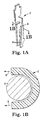
- Figure 1A shows an example of a known socket contact 2 having a shank 4 and wipers 6 extending from shank 4. Wipers 6 are bent toward each other so as to capture a contact pin (not shown in Figure 1A) inserted between wipers 6. It is desired to have the centerlines of wipers 6 align with the centerline of contact pin 8, so that uniform normal forces are applied to contact pin 8.
- Figure 1B shows a cross section of socket contact 2 along line 1B-1B of Figure 1A, with a contact pin 8 inserted into socket contact 2.
- contact pin 8 has a diameter of 0,4573 mm (0.018 inch)
- the socket contact 2 has a material width of 0,127 mm (0.005 inch)
- wipers 6 have a half-width of 0,127 mm (0.0055 inch)
- a clearance of 0,254 mm (0.001 inch) is provided between shank 6 of contact pin 8 and socket contact 2.
- the centerline of socket contact 2 thus has a radius R of 0,3175 mm (0.0125 inch) from the center of contact pin 8.
- the singulation width is the amount of material needed to account for separation of the individual contacts.
- a flat blank width of 1,3792 mm (0.0543 inch) is required.
- the pitch of the connector is 1,27 mm (0.05 inch), for example, there will be a material shortage of 0,1092 mm (0.0043 inch), and the centerlines of wipers 6 of the formed socket contact 2 will not be positioned opposite each other on the centerline of contact pin 8.
- socket contacts stamped on connector pitch when the pitch is less than or equal to the maximum pin diameter times pi.
- International Publication No. WO 9630969 nests the contact spring arms by staggering their position along the pin insertion axis.
- the resulting geometry provides a formed contact having one rigid contact beam and one compliant contact beam, with the contact points of the beams being offset along the pin insertion axis.
- the offset contact points cause unequal normal forces to be applied to the contact pin, which in turn results in undesirable pivoting of the contact on the pin.
- the contact body is stamped with a compliant waist having a reduced cross section.
- the reduced cross section of the contact causes current crowding in the area of the waist, and further encourages undesirable pivoting of the contact on the pin.
- a contact of this type includes a pair of resilient beams configured to grasp a conductive pin therebetween.
- the beams are disposed to contact opposite sides of a conductive pin inserted into the connector, and are formed to produce a contact force sufficiently low to allow easy pin insertion while at the same time providing the required contact force for long term ohmic contact upon insertion of the pin.
- the contact force must be sufficiently low to prevent undesirably high insertion force, plating wear, and bending of the pins during insertion while accommodating some variance in the positioning of individual pins, but high enough to ensure consistent electrical contact with the pin.
- Dual beam sockets are disclosed, for example, in U.S. Patent Nos. 4,140,361; 4,591,230; 4,607,907; and 4,702,545.
- the invention provides an electrical socket contact according to claim 1, an electrical connector according to claim 8 and a method of forming an electrical socket contact according to claim 16.
- the socket contact can be formed by stamping a flat metal sheet to produce a plurality of such contacts having a small center-to-center spacing.
- the inventive contact can be stamped on connector pitch when the pitch is less than or equal to pi times the maximum diameter of the contact pin, while still allowing the centerline of the beams to intersect the centerline of the contact pin.
- a preferred embodiment of the contact includes a body portion from which a shank extends.
- a first beam and a second beam extend from the shank.
- a central reference plane is coincident with the pin insertion axis and centrally located between the first beam and the second beam.
- the first and second beams may form mirror images of each other about the central plane. When viewed from a direction normal to the central plane, first beam and the second beam intersect the pin insertion axis at an acute angle.
- the electrical socket contact may be inserted into an electrical connector housing having a contact receptacle for receiving the socket contact.
- the housing may have a plurality of contact receptacles for receiving a plurality of socket contacts.
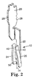
- Figure 2 illustrates a preferred embodiment of a dual beam socket contact 10 according to the present invention.
- the contact 10 is formed by stamping a pattern for a plurality of such contacts in a flat metal blank and then bending portions of the contact blank to form the final contact structure as illustrated in Figure 2.
- the socket contact 10 is adapted for receiving a contact pin (not shown in Figure 2) along a pin insertion axis 14.
- Pin insertion axis 14 coincides with the centerline of the contact pin.
- Socket contact 10 includes a body portion 20, a shank 22, a first beam 24, and a second beam 26.
- Body portion 20, at the rear end of the socket contact 10, is an enlarged portion by which the contact 10 will be securely held in a receptacle of a connector housing (not shown).
- Such connector housing and receptacle are typically made of a thermoplastic material, and are described in greater detail below.
- body portion 20 is provided with barbs 28 for engaging the receptacle walls and thereby assisting the retention of contact 10 within the receptacle.
- socket contact 10 is stamped from a flat metal blank.
- a plurality of socket contact blanks 30 are connected by a carrier strip 31 which carries the socket contact blanks 30 through the subsequent bending and shaping steps which form the finished contact 10.
- the socket contact blanks 30 are separated by a distance 32 which is equal to the pitch of the connector. In this manner, it is possible to gang-insert finished socket contacts 10 into contact receptacles in a connector housing. After insertion, the carrier strip is removed from the socket contacts and disposed.
- Socket contact blank 30 defines a base plane and includes the above-mentioned body portion 20, shank 22, first beam 24 and second beam 26.
- First beam 24 and second beam 26 form mirror images of each other about a central plane 33 which extends between the first and second beams 22, 24 and is normal to the base plane defined by the contact blank 30.
- First beam 24 and second beam 26 each include a free distal end 34 and a proximal end 36 which is cantilevered to shank 22. It will be noted that prior to forming the finished socket contact 10, first beam 24 and second beam 26 are in parallel alignment with shank 22, and the contact points 38 of first beam 24 and second beam 26 are spaced from shank 22 by a distance 40. To form the finished contact 10, a series of bending and shaping steps is performed.
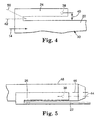
- FIG. 4 A greatly enlarged portion of a contact blank 30, showing only a single contact beam 24, is illustrated in Figure 4.
- the contact is shaped by bending first beam 24 along line 42, while second beam 26 (not shown) is bent along a like line on the opposite half of the blank 30.
- first beam 24 and second beam 26 are made generally perpendicular to the base plane of contact blank 30.
- First beam 24 and second beam 26 typically also undergo additional shaping, as seen in Figure 2, to provide a ramped surface 43 for engaging a contact pin therebetween.
- Figure 5 illustrates the "material shortage" problem (described above in the Background section and further illustrated in Figure 1B) which occurs when the connector pitch is less than or equal to the maximum pin diameter times pi. The material shortage results in the beam contact points 38 failing to align with the pin centerline 46.
- first beam 24 and second beam 26 are not positioned absolutely opposite each other on the pin centerline, the beams exert nonuniform normal forces on the pin which may damage the pin and which also encourage undesirable contact rotation. Additionally, when the beam contact point does not align with the pin centerline, only the edge of the beam tends to contact the pin. This is undesirable because, as the contact ages, corrosion tends to develop and reduce the effective contact area of electrical contact. When only the edge of the beam is in contact with the pin, the initial contact area is much smaller, and the eventual corrosion thus impacts the connection performance in a shorter period of time. This problem is exacerbated by the tendency of such corrosion to initiate at the edges of the beam.
- first beam 24 is bent along a divergent line 50 which forms an acute angle with pin insertion axis 14 when viewed from a direction normal to the base plane (defined by contact blank 30). Bending first beam 22 along line 50 cants or angles first beam 24 upward from the plane of shank 22 to enable first beam 24 to engage mating contact pin 48 along the pin centerline 46.
- opposing second beam 26 is bent along a similar divergent line on the opposite half of the contact blank 30. As best seen in Figure 6, the divergent bend line 50 moves the contact point 38 of the first and second beams 24, 26 into engagement with the centerline 46 of the mating pin 48, and causes first and second beams 22, 24 to form an acute angle with pin centerline 46.
- the bending along divergent line 50 thus permits the design of contacts which can be stamped on socket pitch while keeping the beam contact point 38 coincident with the pin centerline 46.
- the invention thus employs a novel socket contact geometry to overcome the material shortage problem encountered by other socket contacts, when the connector pitch is less than or equal to the maximum pin diameter times pi.
- first beam 24 along divergent line 50 provides other significant advantages to the inventive socket contact.
- the contact 10 is provided with a funnel-shaped lead-in for pin 48.
- the funnel-shaped lead-in eases the entry of pin 48 into socket contact 10 and helps prevent stubbing of pin 48 on the end of contact 10.
- a further advantage of the canted contact beam is shown in Figure 6.
- a canted beam provides a wider target area for contact pin 48 than would a beam which is formed to align in parallel with the axis of pin 48.
- a canted beam presents a target area of width 52 for pin 48, while the same beam, if it were aligned in parallel with the axis 46 of pin 48, would only present a target area of width 54.
- the canted beam of the present invention is therefor more tolerant of pin-to-socket misalignment than conventional socket contacts having identically sized contact beams.
- a narrower canted contact beam can present the same target area as a wider beam which is aligned with the pin axis.
- FIG. 7 An alternative embodiment of the socket contact is shown in Figure 7.
- contact beams 24, 26 have been bent in the conventional manner (as illustrated in Figure 5), and a transverse bend 60 has beer. made in shank 22 such that the axis 44 of the beam diverges at an acute angle from the base plane defined by the contact blank. In this manner, the axis 44 of the beam is caused to intersect the centerline 46 of pin 48 (when viewed from a direction normal to central plane 33) and thereby provide the same benefits as described above for the preferred embodiment.
- shank 22 of socket contact 10, 10' have a stiffening feature which reduces flexure of shank 22 along its longitudinal axis.
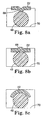
- Figures 8a-8c schematically illustrate a cross sectional view of shank 22 and contact pin 48 when the contact is positioned in a connector receptacle 70. Clearances between pin 48 and shank 22 are not shown for simplification. Stiffening features known to be used in prior art contacts are shown in Figures 8a and 8b. As can be seen, shank 22 in Figures 8a and 8b is provided with a sharp ridge 68 extending along the longitudinal axis of shank 22 (which extends into the plane of the Figures).
- Ridge 68 successfully reduces the ability of shank 22 to flex along its longitudinal axis, but produces several disadvantages as well. Specifically, ridge 68 requires that receptacle 70 which receives the contact be made large enough to accommodate ridge 68 on shank 22. As connector pitch becomes smaller, the wall thickness between adjacent receptacles becomes correspondingly thinner. This in turn leads to reduced strength of the connector housing 72, and greater difficulty in molding the connector housing 72. It is therefor desirable to reduce the size of receptacle 70, and thereby permit greater wall thickness and easier component molding.
- contact 10, 10' of the present invention is preferably provided with a shank 22 having a curved cross-section which follows the contour of pin 48, as illustrated in Figure 8c.
- the curved cross section of shank 22 shown in Figure 8c reduces the ability of shank 22 to flex along its longitudinal axis, while at the same time allowing receptacle 70 to be reduced in size.
- the latter benefit is clearly seen when comparing Figure 8c to Figures 8a and 8b, where the size of each receptacle 70 is identical in each of Figures 8a-8c.
- the contact in Figure 8c having the shank with a curved cross section is capable of fitting within the receptacle 70, while the contacts of Figures 8a and 8b do not fit within the confines of receptacle 70.
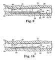
- FIG. 9 there is shown a portion of a receptacle 70 which contains a socket contact 10 according to the invention.
- Figure 9 shows the receptacle with the preferred socket contact of Figures 2 and 5, while Figure 10 shows the alternative embodiment of the socket contact of Figure 7.
- the receptacle 70 is formed in a housing 72 adapted to provide a plurality of receptacles 70 and to thereby hold a plurality of contacts 10. It will be understood that housing 72 includes a plurality of receptacles 70 which are spaced apart in a direction perpendicular to the plane of Figures 9 and 10.
- housing 72 may include multiple receptacles 70 in the plane of Figures 9 and 10, although only a single receptacle 70 is shown.
- Housing 72 includes a pin contact receiving opening 74 at one end of receptacle 70.
- Formed contact 10 is inserted into receptacle 70 in the direction of arrow 76 (opposite pin insertion direction 14) and is retained in receptacle 70 by several features.
- receptacle 70 includes a recessed area 78 for receiving contact 10. As contact 10 is inserted into receptacle 70, shank 22 of contact 10 slides into recessed area 78. Back edge 80 of shank 22 then abuts lip 82 of recessed area 78 and is prevented from moving out of receptacle 70.
- Barbs 28 also provide a retaining force by engaging the softer material of housing 72.
- Receptacle 70 is preferably provided with a beam constraint 84.
- Beam constraint 84 is positioned within receptacle 70 to prevent shank 22 from bending out of alignment and presenting a "stubbing" condition to contact pin 48. Beam constraint 84 also minimizes vibration of the contact during, for example, ultrasonic welding operations which are performed with the finished connector. If the contact vibrates excessively, the contact may crack or be damaged in some other manner.
- Beam constraint 84 may be positioned on only a single side of pin 48, or alternatively a beam constraint 84 may be positioned on each side of an inserted contact pin 48.
Landscapes
- Coupling Device And Connection With Printed Circuit (AREA)
- Manufacturing Of Electrical Connectors (AREA)
Applications Claiming Priority (3)
| Application Number | Priority Date | Filing Date | Title |
|---|---|---|---|
| US990037 | 1997-12-12 | ||
| US08/990,037 US6000975A (en) | 1997-12-12 | 1997-12-12 | Canted beam electrical contact and receptacle housing therefor |
| PCT/US1998/007513 WO1999031767A1 (en) | 1997-12-12 | 1998-04-13 | Electrical female contact with inclined contact arms |
Publications (2)
| Publication Number | Publication Date |
|---|---|
| EP1044484A1 EP1044484A1 (en) | 2000-10-18 |
| EP1044484B1 true EP1044484B1 (en) | 2003-06-25 |
Family
ID=25535689
Family Applications (1)
| Application Number | Title | Priority Date | Filing Date |
|---|---|---|---|
| EP98918204A Expired - Lifetime EP1044484B1 (en) | 1997-12-12 | 1998-04-13 | Electrical female contact with inclined contact arms |
Country Status (6)
| Country | Link |
|---|---|
| US (1) | US6000975A (enExample) |
| EP (1) | EP1044484B1 (enExample) |
| JP (1) | JP2002509344A (enExample) |
| DE (1) | DE69815895T2 (enExample) |
| MY (1) | MY115620A (enExample) |
| WO (1) | WO1999031767A1 (enExample) |
Families Citing this family (7)
| Publication number | Priority date | Publication date | Assignee | Title |
|---|---|---|---|---|
| US6491553B2 (en) * | 2000-12-20 | 2002-12-10 | Berg Technology, Inc. | Electrical connector having an electrical contact with a formed solder cup |
| US6532654B2 (en) * | 2001-01-12 | 2003-03-18 | International Business Machines Corporation | Method of forming an electrical connector |
| US6595799B2 (en) * | 2001-12-19 | 2003-07-22 | Taiwan Gamma Electronic Inc. | Structure of contact piece for cable television signals |
| US8033834B2 (en) * | 2006-12-28 | 2011-10-11 | Hon Hai Precision Ind. Co., Ltd. | Electrical connector terminal with twisted arm |
| US20080160841A1 (en) * | 2006-12-28 | 2008-07-03 | Hon Hai Precision Ind. Co., Ltd. | Electrical contact used in an electrical socket |
| US7645151B2 (en) * | 2007-03-22 | 2010-01-12 | Tyco Electronics Corporation | Shunted electrical connector and shunt therefore |
| DE102011000512B4 (de) | 2011-02-04 | 2021-08-12 | Phoenix Contact Gmbh & Co. Kg | Schleifkontakt |
Family Cites Families (36)
| Publication number | Priority date | Publication date | Assignee | Title |
|---|---|---|---|---|
| BE561443A (enExample) * | 1956-10-08 | |||
| DE2226561A1 (de) * | 1972-05-31 | 1973-12-13 | Bunker Ramo | Gabelkontakt |
| US4140361A (en) * | 1975-06-06 | 1979-02-20 | Sochor Jerzy R | Flat receptacle contact for extremely high density mounting |
| GB1541365A (en) * | 1977-01-05 | 1979-02-28 | Molex Inc | Electrical connector assembly |
| US4379611A (en) * | 1980-11-03 | 1983-04-12 | Hughes Aircraft Company | Connector with low force socket contact having an integral hood |
| US4480386A (en) * | 1982-07-08 | 1984-11-06 | E. I. Du Pont De Nemours And Company | Process for producing dual beam electrical contact |
| DE3424072A1 (de) * | 1984-06-29 | 1986-01-09 | Grote & Hartmann | Steckverbinder |
| US4591230A (en) * | 1984-06-29 | 1986-05-27 | Frank Roldan | Electrical connector receptacle |
| CA1242336A (en) * | 1984-08-16 | 1988-09-27 | Winnipeg Rh Institute Inc. (The) | Sight tube for monitoring of fluids |
| US4607907A (en) * | 1984-08-24 | 1986-08-26 | Burndy Corporation | Electrical connector requiring low mating force |
| JPS6231886U (enExample) * | 1985-08-12 | 1987-02-25 | ||
| JPH0323666Y2 (enExample) * | 1985-11-30 | 1991-05-23 | ||
| US4776651A (en) * | 1985-12-06 | 1988-10-11 | Amp Incorporated | Socket contacts |
| EP0226952B1 (de) * | 1985-12-13 | 1990-03-21 | Siemens Aktiengesellschaft | Kontaktfeder |
| US4722704A (en) * | 1986-06-12 | 1988-02-02 | Amp Incorporated | High density socket contact receptacle |
| US4687278A (en) * | 1986-07-31 | 1987-08-18 | Amp Incorporated | Contact socket with improved contact force |
| US4874338A (en) * | 1987-03-31 | 1989-10-17 | Amp Incorporated | Receptacle box terminal with improved contact area |
| US4772234A (en) * | 1987-07-29 | 1988-09-20 | Amp Incorporated | Terminal for establishing electrical contact with a post |
| GB8721575D0 (en) * | 1987-09-14 | 1987-10-21 | Amp Hollard Bv | Low wear contact system |
| JPH0256882A (ja) * | 1988-08-23 | 1990-02-26 | Yazaki Corp | コンセントおよびその成形方法 |
| US4975084A (en) * | 1988-10-17 | 1990-12-04 | Amp Incorporated | Electrical connector system |
| US4909746A (en) * | 1989-05-31 | 1990-03-20 | Amp Incorporated | Contact for stackable electrical connector |
| GB8926239D0 (en) * | 1989-11-21 | 1990-01-10 | Amp Gmbh | Low insertion force receptacle contact |
| EP0456858B1 (de) * | 1990-05-16 | 1993-09-15 | Siemens Aktiengesellschaft | Erdungsvorrichtung |
| JPH0458474A (ja) * | 1990-06-26 | 1992-02-25 | Witco Of Jupiter Dentsu Kk | 小型コネクタ用雌型接触子とその製造方法 |
| GB9014410D0 (en) * | 1990-06-28 | 1990-08-22 | Perry Forbes G D | Torque-splitting differential drive apparatus |
| US5183421A (en) * | 1991-07-24 | 1993-02-02 | Foxconn International, Inc. | Connector contact and method of manufacture |
| JPH0675417B2 (ja) * | 1992-05-21 | 1994-09-21 | 山一電機株式会社 | ソケットコンタクト |
| US5334053A (en) * | 1992-10-19 | 1994-08-02 | Burndy Corporation | Dual-beam electrical contact with preload tabs |
| US5472358A (en) * | 1994-04-01 | 1995-12-05 | Genrife Company Limited | Contact of single pitch arrangement in strip stock |
| FR2719163A1 (fr) * | 1994-04-22 | 1995-10-27 | Amp France | Borne anti-corrosion par usure, destinée à recevoir une borne complémentaire. |
| JPH0864315A (ja) * | 1994-08-02 | 1996-03-08 | Molex Inc | リセプタクル型電気コネクタ |
| US5672084A (en) * | 1995-03-29 | 1997-09-30 | Elco Corporation | High density connector receptacle |
| DE19517353C1 (de) * | 1995-05-11 | 1996-04-04 | Siemens Ag | Kontaktfeder |
| JP2746862B2 (ja) * | 1995-12-28 | 1998-05-06 | 山一電機株式会社 | コンタクト |
| JP2820916B2 (ja) * | 1996-01-26 | 1998-11-05 | 山一電機株式会社 | 三接片形コンタクトにおける絡み防止機構 |
-
1997
- 1997-12-12 US US08/990,037 patent/US6000975A/en not_active Expired - Fee Related
-
1998
- 1998-04-13 JP JP2000539555A patent/JP2002509344A/ja not_active Withdrawn
- 1998-04-13 EP EP98918204A patent/EP1044484B1/en not_active Expired - Lifetime
- 1998-04-13 WO PCT/US1998/007513 patent/WO1999031767A1/en not_active Ceased
- 1998-04-13 DE DE69815895T patent/DE69815895T2/de not_active Expired - Fee Related
- 1998-11-18 MY MYPI98005228A patent/MY115620A/en unknown
Also Published As
| Publication number | Publication date |
|---|---|
| WO1999031767A1 (en) | 1999-06-24 |
| JP2002509344A (ja) | 2002-03-26 |
| DE69815895T2 (de) | 2004-06-03 |
| EP1044484A1 (en) | 2000-10-18 |
| DE69815895D1 (de) | 2003-07-31 |
| MY115620A (en) | 2003-07-31 |
| US6000975A (en) | 1999-12-14 |
Similar Documents
| Publication | Publication Date | Title |
|---|---|---|
| US5152700A (en) | Printed circuit board connector system | |
| EP0337659B1 (en) | Solder post retention means | |
| EP1624533B1 (en) | Contact for electrical component | |
| US4789346A (en) | Solder post alignment and retention system | |
| US4591230A (en) | Electrical connector receptacle | |
| US4973273A (en) | Dual-beam receptacle socket contact | |
| EP1004152B1 (en) | Electrical connector assembly | |
| US6024612A (en) | Receptacle contact | |
| US6835097B2 (en) | Connector | |
| EP0883916B1 (en) | Electrical connector | |
| US5672084A (en) | High density connector receptacle | |
| EP0657959A1 (en) | Electrical connector assembly for mounting on a printed circuit board | |
| EP1044484B1 (en) | Electrical female contact with inclined contact arms | |
| CA2328658C (en) | Connector contact and method of manufacturing the same | |
| US20030176112A1 (en) | Connector | |
| US5630733A (en) | Female terminal | |
| US4752246A (en) | Preloaded spring contact electrical terminal | |
| US6364722B1 (en) | Female metal terminal | |
| EP0806813B1 (en) | Electrical connector having terminals with improved retention means | |
| EP0314716B1 (en) | Electrical connector with shunt | |
| US7070451B2 (en) | Card connector | |
| WO2007089879A1 (en) | Contact with improved retention member | |
| EP0514066B1 (en) | Electrical connector with improved retention feature | |
| EP0087894A1 (en) | Electrical contact member with a pair of resilient cantilever contact arms | |
| EP1107379A1 (en) | Terminal for detecting incomplete insertion |
Legal Events
| Date | Code | Title | Description |
|---|---|---|---|
| PUAI | Public reference made under article 153(3) epc to a published international application that has entered the european phase |
Free format text: ORIGINAL CODE: 0009012 |
|
| 17P | Request for examination filed |
Effective date: 20000518 |
|
| AK | Designated contracting states |
Kind code of ref document: A1 Designated state(s): DE FR GB IT |
|
| 17Q | First examination report despatched |
Effective date: 20010412 |
|
| GRAH | Despatch of communication of intention to grant a patent |
Free format text: ORIGINAL CODE: EPIDOS IGRA |
|
| RIC1 | Information provided on ipc code assigned before grant |
Free format text: 7H 01R 13/115 A, 7H 01R 12/16 B |
|
| GRAH | Despatch of communication of intention to grant a patent |
Free format text: ORIGINAL CODE: EPIDOS IGRA |
|
| GRAA | (expected) grant |
Free format text: ORIGINAL CODE: 0009210 |
|
| AK | Designated contracting states |
Designated state(s): DE FR GB IT |
|
| REG | Reference to a national code |
Ref country code: GB Ref legal event code: FG4D |
|
| REF | Corresponds to: |
Ref document number: 69815895 Country of ref document: DE Date of ref document: 20030731 Kind code of ref document: P |
|
| PLBE | No opposition filed within time limit |
Free format text: ORIGINAL CODE: 0009261 |
|
| STAA | Information on the status of an ep patent application or granted ep patent |
Free format text: STATUS: NO OPPOSITION FILED WITHIN TIME LIMIT |
|
| ET | Fr: translation filed | ||
| 26N | No opposition filed |
Effective date: 20040326 |
|
| PGFP | Annual fee paid to national office [announced via postgrant information from national office to epo] |
Ref country code: GB Payment date: 20050406 Year of fee payment: 8 |
|
| PGFP | Annual fee paid to national office [announced via postgrant information from national office to epo] |
Ref country code: FR Payment date: 20050418 Year of fee payment: 8 |
|
| PGFP | Annual fee paid to national office [announced via postgrant information from national office to epo] |
Ref country code: DE Payment date: 20050531 Year of fee payment: 8 |
|
| PG25 | Lapsed in a contracting state [announced via postgrant information from national office to epo] |
Ref country code: GB Free format text: LAPSE BECAUSE OF NON-PAYMENT OF DUE FEES Effective date: 20060413 |
|
| PGFP | Annual fee paid to national office [announced via postgrant information from national office to epo] |
Ref country code: IT Payment date: 20060430 Year of fee payment: 9 |
|
| PG25 | Lapsed in a contracting state [announced via postgrant information from national office to epo] |
Ref country code: DE Free format text: LAPSE BECAUSE OF NON-PAYMENT OF DUE FEES Effective date: 20061101 |
|
| GBPC | Gb: european patent ceased through non-payment of renewal fee |
Effective date: 20060413 |
|
| REG | Reference to a national code |
Ref country code: FR Ref legal event code: ST Effective date: 20061230 |
|
| PG25 | Lapsed in a contracting state [announced via postgrant information from national office to epo] |
Ref country code: FR Free format text: LAPSE BECAUSE OF NON-PAYMENT OF DUE FEES Effective date: 20060502 |
|
| PG25 | Lapsed in a contracting state [announced via postgrant information from national office to epo] |
Ref country code: IT Free format text: LAPSE BECAUSE OF NON-PAYMENT OF DUE FEES Effective date: 20070413 |