EP1042814B1 - Hybrid semiconductor imaging device - Google Patents
Hybrid semiconductor imaging device Download PDFInfo
- Publication number
- EP1042814B1 EP1042814B1 EP98963497A EP98963497A EP1042814B1 EP 1042814 B1 EP1042814 B1 EP 1042814B1 EP 98963497 A EP98963497 A EP 98963497A EP 98963497 A EP98963497 A EP 98963497A EP 1042814 B1 EP1042814 B1 EP 1042814B1
- Authority
- EP
- European Patent Office
- Prior art keywords
- readout
- detector
- substrate
- substrates
- cell
- Prior art date
- Legal status (The legal status is an assumption and is not a legal conclusion. Google has not performed a legal analysis and makes no representation as to the accuracy of the status listed.)
- Expired - Lifetime
Links
- 238000003384 imaging method Methods 0.000 title claims abstract description 67
- 239000004065 semiconductor Substances 0.000 title claims description 23
- 239000000758 substrate Substances 0.000 claims abstract description 184
- 238000000034 method Methods 0.000 claims description 13
- 238000012546 transfer Methods 0.000 claims description 11
- 238000004519 manufacturing process Methods 0.000 claims description 4
- 230000006335 response to radiation Effects 0.000 claims description 3
- 230000005855 radiation Effects 0.000 description 24
- 238000013459 approach Methods 0.000 description 10
- 238000009825 accumulation Methods 0.000 description 6
- 230000002950 deficient Effects 0.000 description 6
- 238000001514 detection method Methods 0.000 description 6
- 238000005516 engineering process Methods 0.000 description 6
- FVAUCKIRQBBSSJ-UHFFFAOYSA-M sodium iodide Chemical compound [Na+].[I-] FVAUCKIRQBBSSJ-UHFFFAOYSA-M 0.000 description 6
- 239000000463 material Substances 0.000 description 5
- 229910052710 silicon Inorganic materials 0.000 description 5
- MARUHZGHZWCEQU-UHFFFAOYSA-N 5-phenyl-2h-tetrazole Chemical compound C1=CC=CC=C1C1=NNN=N1 MARUHZGHZWCEQU-UHFFFAOYSA-N 0.000 description 4
- 102220565243 L-lactate dehydrogenase A-like 6A_M11A_mutation Human genes 0.000 description 4
- XUIMIQQOPSSXEZ-UHFFFAOYSA-N Silicon Chemical compound [Si] XUIMIQQOPSSXEZ-UHFFFAOYSA-N 0.000 description 4
- QWUZMTJBRUASOW-UHFFFAOYSA-N cadmium tellanylidenezinc Chemical compound [Zn].[Cd].[Te] QWUZMTJBRUASOW-UHFFFAOYSA-N 0.000 description 4
- 238000002161 passivation Methods 0.000 description 4
- 238000012545 processing Methods 0.000 description 4
- 239000010703 silicon Substances 0.000 description 4
- 239000011159 matrix material Substances 0.000 description 3
- PXHVJJICTQNCMI-UHFFFAOYSA-N Nickel Chemical compound [Ni] PXHVJJICTQNCMI-UHFFFAOYSA-N 0.000 description 2
- VYPSYNLAJGMNEJ-UHFFFAOYSA-N Silicium dioxide Chemical compound O=[Si]=O VYPSYNLAJGMNEJ-UHFFFAOYSA-N 0.000 description 2
- 239000000853 adhesive Substances 0.000 description 2
- 230000001070 adhesive effect Effects 0.000 description 2
- ORCSMBGZHYTXOV-UHFFFAOYSA-N bismuth;germanium;dodecahydrate Chemical compound O.O.O.O.O.O.O.O.O.O.O.O.[Ge].[Ge].[Ge].[Bi].[Bi].[Bi].[Bi] ORCSMBGZHYTXOV-UHFFFAOYSA-N 0.000 description 2
- 239000004020 conductor Substances 0.000 description 2
- 230000000694 effects Effects 0.000 description 2
- PCHJSUWPFVWCPO-UHFFFAOYSA-N gold Chemical compound [Au] PCHJSUWPFVWCPO-UHFFFAOYSA-N 0.000 description 2
- 229910052737 gold Inorganic materials 0.000 description 2
- 239000010931 gold Substances 0.000 description 2
- 229910052738 indium Inorganic materials 0.000 description 2
- APFVFJFRJDLVQX-UHFFFAOYSA-N indium atom Chemical compound [In] APFVFJFRJDLVQX-UHFFFAOYSA-N 0.000 description 2
- 238000005304 joining Methods 0.000 description 2
- BASFCYQUMIYNBI-UHFFFAOYSA-N platinum Chemical compound [Pt] BASFCYQUMIYNBI-UHFFFAOYSA-N 0.000 description 2
- 238000003908 quality control method Methods 0.000 description 2
- 238000002601 radiography Methods 0.000 description 2
- 235000009518 sodium iodide Nutrition 0.000 description 2
- BYHQTRFJOGIQAO-GOSISDBHSA-N 3-(4-bromophenyl)-8-[(2R)-2-hydroxypropyl]-1-[(3-methoxyphenyl)methyl]-1,3,8-triazaspiro[4.5]decan-2-one Chemical compound C[C@H](CN1CCC2(CC1)CN(C(=O)N2CC3=CC(=CC=C3)OC)C4=CC=C(C=C4)Br)O BYHQTRFJOGIQAO-GOSISDBHSA-N 0.000 description 1
- JBRZTFJDHDCESZ-UHFFFAOYSA-N AsGa Chemical compound [As]#[Ga] JBRZTFJDHDCESZ-UHFFFAOYSA-N 0.000 description 1
- 238000010521 absorption reaction Methods 0.000 description 1
- 238000007792 addition Methods 0.000 description 1
- 229910052782 aluminium Inorganic materials 0.000 description 1
- 239000004411 aluminium Substances 0.000 description 1
- XAGFODPZIPBFFR-UHFFFAOYSA-N aluminium Chemical compound [Al] XAGFODPZIPBFFR-UHFFFAOYSA-N 0.000 description 1
- 230000015572 biosynthetic process Effects 0.000 description 1
- 239000003990 capacitor Substances 0.000 description 1
- 238000011976 chest X-ray Methods 0.000 description 1
- 238000004140 cleaning Methods 0.000 description 1
- 238000010276 construction Methods 0.000 description 1
- PMHQVHHXPFUNSP-UHFFFAOYSA-M copper(1+);methylsulfanylmethane;bromide Chemical compound Br[Cu].CSC PMHQVHHXPFUNSP-UHFFFAOYSA-M 0.000 description 1
- 239000013078 crystal Substances 0.000 description 1
- 238000013500 data storage Methods 0.000 description 1
- 230000007423 decrease Effects 0.000 description 1
- 230000001066 destructive effect Effects 0.000 description 1
- 230000005669 field effect Effects 0.000 description 1
- 229910052732 germanium Inorganic materials 0.000 description 1
- GNPVGFCGXDBREM-UHFFFAOYSA-N germanium atom Chemical compound [Ge] GNPVGFCGXDBREM-UHFFFAOYSA-N 0.000 description 1
- XMBWDFGMSWQBCA-UHFFFAOYSA-N hydrogen iodide Chemical compound I XMBWDFGMSWQBCA-UHFFFAOYSA-N 0.000 description 1
- LQBJWKCYZGMFEV-UHFFFAOYSA-N lead tin Chemical compound [Sn].[Pb] LQBJWKCYZGMFEV-UHFFFAOYSA-N 0.000 description 1
- 230000008774 maternal effect Effects 0.000 description 1
- 238000012986 modification Methods 0.000 description 1
- 230000004048 modification Effects 0.000 description 1
- 229910052759 nickel Inorganic materials 0.000 description 1
- 238000009659 non-destructive testing Methods 0.000 description 1
- NJPPVKZQTLUDBO-UHFFFAOYSA-N novaluron Chemical class C1=C(Cl)C(OC(F)(F)C(OC(F)(F)F)F)=CC=C1NC(=O)NC(=O)C1=C(F)C=CC=C1F NJPPVKZQTLUDBO-UHFFFAOYSA-N 0.000 description 1
- 230000003071 parasitic effect Effects 0.000 description 1
- 239000002245 particle Substances 0.000 description 1
- 229910052697 platinum Inorganic materials 0.000 description 1
- 230000004044 response Effects 0.000 description 1
- 230000035945 sensitivity Effects 0.000 description 1
- 235000012239 silicon dioxide Nutrition 0.000 description 1
- 239000000377 silicon dioxide Substances 0.000 description 1
- 229910000679 solder Inorganic materials 0.000 description 1
- 238000003860 storage Methods 0.000 description 1
- 238000013519 translation Methods 0.000 description 1
Images


Classifications
-
- H—ELECTRICITY
- H10—SEMICONDUCTOR DEVICES; ELECTRIC SOLID-STATE DEVICES NOT OTHERWISE PROVIDED FOR
- H10F—INORGANIC SEMICONDUCTOR DEVICES SENSITIVE TO INFRARED RADIATION, LIGHT, ELECTROMAGNETIC RADIATION OF SHORTER WAVELENGTH OR CORPUSCULAR RADIATION
- H10F39/00—Integrated devices, or assemblies of multiple devices, comprising at least one element covered by group H10F30/00, e.g. radiation detectors comprising photodiode arrays
- H10F39/011—Manufacture or treatment of image sensors covered by group H10F39/12
- H10F39/018—Manufacture or treatment of image sensors covered by group H10F39/12 of hybrid image sensors
-
- H—ELECTRICITY
- H10—SEMICONDUCTOR DEVICES; ELECTRIC SOLID-STATE DEVICES NOT OTHERWISE PROVIDED FOR
- H10F—INORGANIC SEMICONDUCTOR DEVICES SENSITIVE TO INFRARED RADIATION, LIGHT, ELECTROMAGNETIC RADIATION OF SHORTER WAVELENGTH OR CORPUSCULAR RADIATION
- H10F39/00—Integrated devices, or assemblies of multiple devices, comprising at least one element covered by group H10F30/00, e.g. radiation detectors comprising photodiode arrays
- H10F39/10—Integrated devices
- H10F39/12—Image sensors
- H10F39/18—Complementary metal-oxide-semiconductor [CMOS] image sensors; Photodiode array image sensors
- H10F39/184—Infrared image sensors
- H10F39/1843—Infrared image sensors of the hybrid type
-
- H—ELECTRICITY
- H10—SEMICONDUCTOR DEVICES; ELECTRIC SOLID-STATE DEVICES NOT OTHERWISE PROVIDED FOR
- H10F—INORGANIC SEMICONDUCTOR DEVICES SENSITIVE TO INFRARED RADIATION, LIGHT, ELECTROMAGNETIC RADIATION OF SHORTER WAVELENGTH OR CORPUSCULAR RADIATION
- H10F39/00—Integrated devices, or assemblies of multiple devices, comprising at least one element covered by group H10F30/00, e.g. radiation detectors comprising photodiode arrays
- H10F39/10—Integrated devices
- H10F39/12—Image sensors
- H10F39/18—Complementary metal-oxide-semiconductor [CMOS] image sensors; Photodiode array image sensors
- H10F39/189—X-ray, gamma-ray or corpuscular radiation imagers
-
- H—ELECTRICITY
- H10—SEMICONDUCTOR DEVICES; ELECTRIC SOLID-STATE DEVICES NOT OTHERWISE PROVIDED FOR
- H10F—INORGANIC SEMICONDUCTOR DEVICES SENSITIVE TO INFRARED RADIATION, LIGHT, ELECTROMAGNETIC RADIATION OF SHORTER WAVELENGTH OR CORPUSCULAR RADIATION
- H10F39/00—Integrated devices, or assemblies of multiple devices, comprising at least one element covered by group H10F30/00, e.g. radiation detectors comprising photodiode arrays
- H10F39/80—Constructional details of image sensors
- H10F39/809—Constructional details of image sensors of hybrid image sensors
-
- H—ELECTRICITY
- H04—ELECTRIC COMMUNICATION TECHNIQUE
- H04N—PICTORIAL COMMUNICATION, e.g. TELEVISION
- H04N23/00—Cameras or camera modules comprising electronic image sensors; Control thereof
- H04N23/30—Cameras or camera modules comprising electronic image sensors; Control thereof for generating image signals from X-rays
Definitions
- the invention relates to hybrid imaging devices, for example for high energy radiation imaging, for example radiation having energies in excess of 1 keV, such as X-rays.
- CCD-based devices both in stand-alone implementations and coupled to scintillating screens, silicon microstrip detectors and semiconductor pixel detectors.
- Semiconductor pixel detectors such as have been described in the Applicant's International patent application WO95/33332 , based on ASIC (Application Specific Integrated Circuit) CMOS processing, can provide high spatial resolution, direct detection, compactness, high absorption efficiency and real-time imaging.
- limitations (e.g. yield) of ASIC CMOS technology based on, for example, crystalline or polycrystalline semiconductor technology, limit the maximal size of monolithic detectors to a few square centimetres.
- Various methods of combining individual monolithic detectors have been, therefore, proposed. The major challenge is the formation of continuous imaging areas larger than that possible with a single hybrid imaging device without any blind regions
- EP-A-0,577,487 Another approach to large area imaging is described in European patent application EP-A-0,577,487 .
- This approach provides an imaging apparatus comprising several individual detector substrates arranged adjacent to each other and rigidly connected to each other by means of support substrates which overlap adjacent detector substrates The detector substrates are rigidly connected to the support substrates by means of indium bumps. Although the total thickness of the apparatus is independent of the imaging area, the overall structure is, once again rigid. Also, the constructions proposed in EP-A-0,577,487 are likely to suffer from edge effects or inactive regions along the boundaries between two detectors.
- the desired area is around 10 cm 2 and the overall imaging device thickness is highly constrained, preferably under 5 mm, or even better, under 3 mm.
- the present invention seeks to provide a solution to the provision of a hybrid semiconductor imaging array providing an area larger than that possible with prior hybrid imaging devices using CMOS based readout chips without the bulk and complexity and/or requirements for movement or interpolation of the prior art.
- an embodiment of the invention provides an approach to forming an imaging array different from that of the prior art. All prior art approaches are based on methods for joining smaller monolithic detectors into large area mosaics with a plurality of detecting substrates and a plurality of CMOS readout layers. Typically the number of detector substrates and the number of readout substrates are substantially equal.
- an imaging device comprises one detector substrate with a plurality of readout chips connected thereto. No direct contact, either electrical or mechanical, between the readout substrates is needed. The readout substrates are mechanically and electrically connected to the single detector substrate.
- readout circuit(s) on the readout substrate do not need to be aligned directly with the corresponding detector cells, but can be out of register (i.e. offset) with respect thereto, areas of the detector substrate located in a region between readout substrates or over a non-active region of the readout substrates, which would otherwise be inactive or give very poor resolution, can be made active with good resolution.
- An embodiment of the invention can provide an imaging device providing continuous imaging while constraining the detector thickness to a minimum. Also, a relatively large area imaging device can be produced without the readout substrate needing to be so large that manufacturing yield decreases.
- Conductive tracks enable a readout circuit contact to be connected to a detector cell contact offset with respect thereto.
- the plurality of readout substrates are bump-bonded to the readout detector substrate.
- the conductive track(s) can be formed on the second surface of the detector but electrically insulated therefrom by an intermediate insulative layer.
- the conductive track or tracks could alternatively, or additionally be formed on a separate intermediate substrate.
- a support substrate can also be mechanically and electrically connected to the readout substrates.
- the readout substrates can be mechanically and electrically connected to the detector substrate at a first surface of the readout substrates, the readout substrates being mechanically and electrically connected to the support substrate at a second surface of the readout substrates.
- the readout substrates can be bump-bonded to the support substrate. Preferably, however, wire bonds are used for the electrical connections.
- a support substrate or mother board, can be provided for mechanical support of the assembly of the detector substrate and readout substrates and for electrical connection to and readout from the readout substrates.
- the invention also provides an imaging system comprising an imaging device as described above.
- defective semiconductor substrates can be removed after bonding and replaced by new semiconductor substrates.
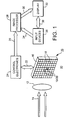
- FIG 1 is a schematic representation of an example of an imaging system 10 as described in the Applicant's International application WO 95/33332 for radiation imaging of an object 12 subjected to radiation 14.
- the radiation may, for example, be X-ray radiation and the object 12 may, for example, be part of a human body.
- the imaging device comprises an imaging array 15 including at least one Active-pixel Semiconductor Imaging Devices (ASID) 16. Although only one ASID 16 is shown schematically in Figure 1 , the imaging array will typically include a plurality of imaging devices 16. Each imaging device 16 provides a plurality of image, or pixel cells 18.
- ASID Active-pixel Semiconductor Imaging Devices
- Each imaging device directly detects high energy incident radiation such as X-rays, ⁇ -rays, ⁇ -rays or ⁇ -rays and accumulates at each pixel cell, by means of a randomly accessible, active, dynamic cell circuit on or adjacent to a corresponding image detector cell, values representative of the radiation incident at that image cell.
- the imaging device 16 can be configured as a single semiconductor substrate (e.g., silicon) with each image, or pixel cell comprising an image detector cell 19 and an active image cell circuit 20, or alternatively on two substrates, one with an array of image detector cells 19 and one with an array of active image cell circuits 20, the substrates being mechanically connected to each other by, for example, microbumps (bump-bonds).
- a single semiconductor substrate e.g., silicon
- pixel cell comprising an image detector cell 19 and an active image cell circuit 20
- the substrates being mechanically connected to each other by, for example, microbumps (bump-bonds).
- Figure 2 is a schematic partial cross-sectional representation of a two-substrate imaging device showing the connection of the substrates.
- Individual detector cells 19 of an image detector substrate 44 are connected to corresponding cell circuits 20 of a readout substrate 42 by means of microbumps 46.
- the cell circuits 20 are schematically represented within the substrate 42 by means of the symbol of a FET.
- the detector substrate 44 is provided with a continuous electrode 50 on the side of the substrate 44 which is exposed to incident radiation. In Figure 2 , therefore, the incident radiation is assumed to arrive in an upwards direction.
- a plurality of detector cell electrodes 54 are provided on the rear surface of the detector substrate 44. It is the array of detector cell electrodes 54 which effectively defines the individual image detector cells 19 within the detector substrate 44.
- a bias voltage is applied to the continuous electrode 50 and image cell detection zones 52 are defined between the continuous electrode 50 and the respective detector cell electrodes 54.
- Each of the detector cell electrodes is electrically and mechanically coupled to a respective cell circuit 20 by a respective microbump 46. It will be appreciated that the representation in Figure 2 is highly schematic, and not to scale.
- a value associated with the electric pulse is then accumulated in an active circuit element, either directly as a charge value or as an equivalent voltage or current value such that new charge created from subsequent incoming radiation is added continuously.
- Examples of possible accumulating devices are an integrated capacitor or the gate of an integrated transistor.
- the charge accumulation process in a cell circuit 20 continues until control signals are issued from control electronics 24 to start a process of reading out information by addressing each cell circuit 20, effectively in a random access manner. During readout of the accumulated charge values, charge continues to be accumulated.
- Cell circuits 20 may selectively be reset after readout to discharge the charge accumulation circuit elements, and only then are image cells inactive for a very short time with practically no dead time
- the cell circuits 20 are provided for each image cell 18 to accumulate charge created in the detector cell when, for example, a photon or a charged particle of radiation is incident on the detection zone of that detector cell 19.
- An active cell circuit 20 and the detector cell 19 can be of the order of a few tens of microns in size (e.g., 10-50 ⁇ m).
- FIG. 3 A schematic representation of an example of a cell circuit is described with reference to Figures 3 .
- This example of a cell circuit uses field effect transistors (FETs) arranged as a cascode connected amplifier.
- FET M11 A 70 and in particular the gate thereof, forms charge accumulation circuitry.
- FET M 11B 72 forms readout circuitry.
- FET M11C 77 forms reset circuitry.
- VBIAS 60 is a bias voltage input across the depletion zone forming a detector cell 19 of the image cell.
- the detector cell 19 is represented by a diode symbol D 11.
- SIGOUT 62 is an analogue signal output and VANA 64 an analogue power supply input.
- RES-R-1 66 is a reset input and ENA-R- 1 68 is an enable input for the cell circuit.
- Charge generated in the detector cell 19 in response to incident radiation is automatically accumulated in the gate of a transistor M 11A 70 when both the RES-R-1 66 and ENA-R-1 68 inputs are low.
- ENA-R-I 68 is taken to a high state, which allows current to flow from the transistor M11A 70 through the transistor M11B 72 to SIGOUT 62.
- the cell circuit is reset by taking RES-R-1 66 to high, whereupon after RES-R-1 66 has been at high for merely a few microseconds, any accumulated charge will have been removed from the gate of the transistor M11A 70. Immediately after RES-R-1 66 goes to a low level, charge can begin to accumulate at the gate of the transistor M11A 70.
- charge accumulation ability can be maximised by arranging that the gate capacitance of a charge accumulation transistor M 11A 70 forms substantially (say greater than 90% of) the input node capacitance (total capacitance) of the detector cell 19, the charge accumulation circuitry 70, the readout circuitry M 11A 72 and reset circuitry 77 of Figure 3 and minimizing the parasitic or unwanted capacitance of all other circuit (and detector) components.
- the M11A 70 capacitance can be 2 pF and the FET gate voltage dynamic range can be at least 2 Volts. This corresponds to about 25,000,000 electrons in storage capacity.
- control electronics 24 includes processing and control circuitry, which is connected to the cell circuits 18 on the semiconductor substrate as represented schematically by the two-way arrow 22.
- the control electronics 24 enable the cell circuits 20 associated with individual image cells 18 to be addressed (e.g., scanned) for reading out charge accumulated in the cell circuits 20 at the individual image cells 18.
- the charge read out is supplied to Analogue to Digital Converters (ADCs) for digitisation and Data Reduction Processors (DRPs) for processing the binary signal.
- ADCs Analogue to Digital Converters
- DRPs Data Reduction Processors
- the control electronics 24 is further interfaced via a path represented schematically by the arrow 26 to an image processor 28.
- the image processor 28 includes data storage in which it stores the digital value representative of the charge read from each image cell along with the position of the image cell 18 concerned. For each image cell 18, each charge value read from the image cell is added to the charge value already stored for that image cell so that a charge value is accumulated. As a result, each image can be stored as a representation of a two-dimensional array of pixel values which can be stored, for example, in a database.
- the image processor 28 can access the stored image data in the database to select a given image (all the array) or a part of the image (a sub-sample of the image array).
- the image processor 28 reads the values stored for the selected image positions and causes a representation of the data to be displayed on a display 32 via a path represented schematically by the arrow 30.
- the data can of course be printed rather than, or in addition to being displayed and can be subjected to further processing operations. For example, background and noise can be subtracted as a constant from each pixel charge value. This pedestal and/or background subtraction is possible if prior to image taking an "empty" image is acquired. For each pixel a background value is deduced and can be subtracted accordingly.
- User input devices 36 connected via paths represented schematically by the arrow 34 and possibly interacting with the display 32 as represented schematically by the double arrow 38 can be used to control the operation of the imaging system.
- the user input devices 36 can include, for example a keyboard, a mouse, etc.
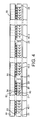
- the imaging device comprising a unitary radiation detector substrate 44, a plurality of readout substrates 42.1 - 42.6 (here 6 readout substrates of which three are visible) and a support substrate 80.
- the unitary radiation detector comprises a semiconductor substrate with one surface having a continuous electrode 50 for applying bias voltage, and the opposite surface having an array of detector cell electrodes, or contacts 54 for collecting charge generated in response to radiation incident for respective radiation detector cells 19.
- the detector cell electrodes 54 form charge collection contacts, which in combination with the bias electrode 50 effectively define detection zones 52 in the semiconductor detector substrate 44 for the individual detector cells.
- the detector substrate material can be, for example, of silicon (Si) or cadmium telluride (CdTe) or cadmium zinc telluride (CdZnTe), lead iodide (PbI), gallium arsenide (GaAs), or germanium (Ge) although other materials can be used.
- CdTe and CdZnTe are more desirable options because of their high sensitivity to X-ray energies used in medical applications and in particular intraoral imaging.
- the electrodes can be formed from gold or other conductors compatible with the substrate material. Passivation can be provided between the detector cell contacts to improve radiation cell definition.
- the plurality of readout substrates 42 each comprise a substrate comprising an array of readout circuits 20 (represented schematically by FET symbols). Respective readout circuit contacts 21 for readout circuits 20 are connected to corresponding detector cells of the detector substrate 44. Each readout substrate 42 is mechanically and electrically connected to the detector substrate 44, preferably by bump-bonds, for example indium bumps or low temperature lead-tin based solder bonds.
- the readout substrate is preferably implemented in CMOS technology using a silicon substrate, although other semiconductor technologies could be used.
- the contacts can be made of aluminium, gold, platinum, nickel or another conductive material or a combination thereof compatible with the semiconductor technology.
- the support substrate 80 forms a mother board for mounting the bonded detector-readout substrate structure and for providing electrical and electronic connection to each readout substrate.
- the bonded detector-readout substrate structure is mechanically attached to the support substrate by giving and is electrically connected to it by means of wire bonds.
- At least one and typically more detector cell electrodes on the detector substrate is out of register with its corresponding readout circuit on a readout substrate.
- at least one detector cell on the detector substrate is not aligned with its corresponding readout cell on a readout substrate
- the readout circuits of a readout substrate may extend to the edges of the readout substrate, but more typically, as illustrated in Figure 4 , the readout circuits do not extend to all four edges of the readout substrate leaving a non-active region 23.
- the edge region of a readout substrate may be occupied by control, decoding and multiplexing circuitry.
- the edge region may be used for making electrical connections (voltages, signals) to the exterior of the substrate.
- detector regions overlying such readout substrate edge regions are kept sensitive to incident radiation in the following manner.
- the readout circuit contacts are aligned with the detector cell contacts to facilitate bump-bonding.
- the detector substrate overlies non-active regions of a readout substrate or a gap between readout substrates this is not the case
- the detector cell contacts for detector substrate regions overlying readout substrate regions not having readout cells are arranged to be connected electrically to readout cell contacts not in alignment with the detector cells.
- each such detector contact is not bump-bonded directly to the readout semiconductor substrate, but is instead connected via a conductive strip 53 extending over the detector surface to a transfer contact (55, see Figure 6 ) aligned with the readout cell contact.
- the conductive strip 53 and the transfer contact 55 are formed on the detector substrate but are insulated from the surface of the detector substrate by an insulating layer 59. A schematic representation of this is described in more detail later with reference to Figure 6 .
- the pixel pitch in detector regions overlying readout substrate regions without readout cell contacts bumps may be different from the pixel pitch elsewhere as can be seen in Figure 4 . This allows, inter alia, for the detector surface taken up by the conductive tracks It should be noted that the same approach of using conductive tracks from detector cell contacts on the detector substrate to further contacts for bonding to readout cell contacts on a readout substrate can also be used to provide image continuity in areas of the detector corresponding to the, albeit small, gaps between the readout substrates.
- the assembly of the detector substrate with a plurality of readout substrates mechanically and electrically connected thereto is mounted on a support substrate.
- the support substrate as well as mechanically supporting the assembly, also provides electrical connections to the readout chips.
- the assembly can be mechanically bonded to the support substrate by adhesives, or other methods, and electrical connections can be made, for example, by means of wire bonds with the readout substrates. Alternatively, mechanical and electrical connections can be made by bump-bonding or other such techniques.
- the readout substrate are bump-bonded to the detector substrate on an upper surface of the readout substrates and are bump-bonded to the support substrate on a lower surface of the readout substrates (not shown in Figure 4 ).
- the support substrate can, for example, be a printed circuit board (PCB).
- Figure 5 is a schematic plan view of one readout substrate formed by a CMOS chip.
- the CMOS readout chip 42 has readout cell circuits in a region 90 with a corresponding array of readout contacts.
- Edge regions 92, 93, 94 and 95 do not include readout circuits and therefore do not include readout cell contacts for bump-bonding
- the edge region 94 is used to allow the connection of wire bonds to the support substrate and should not be covered by the detector substrate.
- the region 92 is reserved for additional circuitry such as control, decoding and multiplexing.
- the regions 92, 93 and 95 however, can be covered by the detector.
- Figure 6 illustrates part of the surface of detector substrate used for contacting the readout substrate.
- a detector cell contact 54 in a region 57 is connected to a transfer contact 55 by a conductive track 53 on the detector substrate 44
- the transfer contact 55 is bump-bonded to a readout cell contact (not shown) on a readout substrate.
- the conductive track 53 can be of any required shape.
- they are electrically insulated from the surface of the detector substrate material by, for example, forming the conductive track and the transfer contact over a layer 59 (shown as a partial layer in Figure 6 ) of passivation (e.g. aluminum nitride or silicon dioxide) or another insulating maternal.
- passivation e.g. aluminum nitride or silicon dioxide
- the passivation material can be provided on the detector substrate surface between all detector cell contacts, with the conductive tracks 53 and transfer contacts 55 simply formed over the passivation layer.
- the region 57 could be a region of the detector substrate overlying one of the readout chip regions 92, 93 or 95 (not shown in Fig. 6 ), or alterative a gap between two adjacent readout chips.
- the conductive track can be formed on or within an intermediate substrate (not shown).
- the regions and the track shown in Figure 6 are for illustrative purposes only and can be configured to a particular application.
- the region 57 does not necessarily extend to an edge of the detector substrate 44, but can be located at any position with respect to the detector and can have any size or shape.
- the entire radiation entrance surface of detector substrate 44 can be sensitive to radiation and the readout substrates 42 can, in combination, be responsive to radiation incident at any position of the detector substrate 44.
- the edge regions 92, 93, 95 of the CMOS readout chips are completely covered by the semiconductor substrate.
- the edge regions 94 of the readout chips are however exposed as illustrated in Fig. 7 , which is a plan view from the radiation receptive surface of the radiation detector, showing the regions 94 of the readout chips 42.1 - 42.6 extending beyond the upper and lower edges (as viewed in Figure 7 ) of the detector substrate 44 for electronic and electrical connections between the readout chips 42.1 - 42.6, and also showing the support substrate 80 and the wire bonds 81.
- the adjacent edges of the readout chips 42.1 - 42.6 do not come into physical contact so as to facilitate the bump-bonding process.
- the gap between the readout chips can be compensated for by regions 57 having translation of the detector cell outputs in the same manner shown in Figure 6 as far as the non-active portions 92, 93 and 95 of the readout chips.
- the detector cell (pixel) pitch in the detector regions 57 may be different from elsewhere.
- the structure comprising the detector substrate 44 and the plurality of readout substrates 42 is mounted on a mother board, or support substrate 80.
- a mother board, or support substrate 80 In order to provide the connections to the support substrate 80, thus extends somewhat beyond the periphery of the readout substrates 42 as shown in Figure 7 .
- the connections between the readout substrates 42 and the support substrate 80 is formed by wire bonds 81 and the readout substrates are secured to the support substrate by adhesives.
- the approximate chip dimensions are 18.13 mm ⁇ 9.65 mm.
- the edge area 94 has dimensions of approximately 0.55 mm ⁇ 9.65 mm so the total active area of semiconductor substrate 42 of Fig. 7 is 35.16 mm ⁇ 28.95 mm.
- the pixel pitch in detector areas overlying CMOS chip areas 20 can be as low as 35 micrometres square and the pixel pitch in areas 92 of the detector can be larger, for example 140 micrometres square, for pixels overlying the edges 92 and 70 micrometres for pixels overlying the edges 93, 95.
- the support substrate 90 extends over sides 24 of readout chips in order to provide for wire bonding connections.
- the support substrate extends no more than 2 mm from each side. More preferably, the board extends no more than 1 mm on each side. Even more preferably, the board extends no more than 0.5 mm on each side.
- the detector thickness can be around 0.3 mm -1.0 mm if the detector is made of Si, or be 0.5 mm - 5.0 mm if the detector is made of CdTe or CdZnTe.
- the CMOS chip is approximately 0.5 mm thick and the support substrate thickness around 0.3 mm - 0.4 mm.
- any number of chips can be arranged in a 2 ⁇ n matrix where n is an integer. Where the readout chip has an exposed edge 94, this constrains the matrix to have the "x2" form with two rows of readout substrates.
- readout chip edge regions 24 need not be exposed.
- electrical and mechanical connection of the readout substrate to the support substrate can be achieved via their common surface (e.g. by means of bump-bonding) with electrical connections running through the readout substrate chip perpendicular to the plane of Figure 6 .
- larger areas can be covered as the chips may be arranged in a matrix of the form m ⁇ n where m and n can be any integers.
- the numbers of detector cell contacts which are not in alignment with their corresponding readout cell contacts may be reduced with respect to the embodiment of Figure 6 .
- detector and readout cells not in register with each other and pixel pitch variations along the imaging surface will typically be encountered.
- a preferred method for fabricating such an imaging device is to bump-bond chips sequentially. Chip quality control would be extremely useful in order to reduce the probability of bonding defective chips. However, defective chips can be removed and, after cleaning of detector contacts, new chips can be bonded.
- each CMOS chip is bump-bonded onto the detector substrate following quality control.
- Defective chips may be subsequently removed after bonding. In that case, contact points on the detector cleaned before a new CMOS chip is bonded.
Landscapes
- Solid State Image Pick-Up Elements (AREA)
- Transforming Light Signals Into Electric Signals (AREA)
- Measurement Of Radiation (AREA)
- Printers Or Recording Devices Using Electromagnetic And Radiation Means (AREA)
- Photographic Developing Apparatuses (AREA)
Applications Claiming Priority (3)
| Application Number | Priority Date | Filing Date | Title |
|---|---|---|---|
| GB9726765 | 1997-12-18 | ||
| GB9726765A GB2332562B (en) | 1997-12-18 | 1997-12-18 | Hybrid semiconductor imaging device |
| PCT/EP1998/007522 WO1999033116A1 (en) | 1997-12-18 | 1998-11-16 | Hybrid semiconductor imaging device |
Publications (2)
| Publication Number | Publication Date |
|---|---|
| EP1042814A1 EP1042814A1 (en) | 2000-10-11 |
| EP1042814B1 true EP1042814B1 (en) | 2010-05-26 |
Family
ID=10823835
Family Applications (1)
| Application Number | Title | Priority Date | Filing Date |
|---|---|---|---|
| EP98963497A Expired - Lifetime EP1042814B1 (en) | 1997-12-18 | 1998-11-16 | Hybrid semiconductor imaging device |
Country Status (9)
| Country | Link |
|---|---|
| US (1) | US6323475B1 (enExample) |
| EP (1) | EP1042814B1 (enExample) |
| JP (1) | JP4112175B2 (enExample) |
| AT (1) | ATE469439T1 (enExample) |
| AU (1) | AU1874599A (enExample) |
| DE (1) | DE69841688D1 (enExample) |
| GB (1) | GB2332562B (enExample) |
| IL (1) | IL136704A (enExample) |
| WO (1) | WO1999033116A1 (enExample) |
Families Citing this family (22)
| Publication number | Priority date | Publication date | Assignee | Title |
|---|---|---|---|---|
| DE19933471A1 (de) * | 1999-07-20 | 2001-02-01 | Daimler Chrysler Ag | Bildaufnehmer mit integrierter Signalverarbeitung und Bildaufnahmeverfahren |
| US7189971B2 (en) * | 2002-02-15 | 2007-03-13 | Oy Ajat Ltd | Radiation imaging device and system |
| US7170062B2 (en) * | 2002-03-29 | 2007-01-30 | Oy Ajat Ltd. | Conductive adhesive bonded semiconductor substrates for radiation imaging devices |
| US6841784B2 (en) * | 2002-07-02 | 2005-01-11 | Ray Therapy Imaging Ab | Radiation sensor device |
| US6844543B2 (en) * | 2002-07-03 | 2005-01-18 | The Regents Of The University Of California | Quantitation of absorbed or deposited materials on a substrate that measures energy deposition |
| US7223981B1 (en) | 2002-12-04 | 2007-05-29 | Aguila Technologies Inc. | Gamma ray detector modules |
| US7247858B2 (en) * | 2003-04-10 | 2007-07-24 | Agfa Healthcare, N.V. | Method for creating a contiguous image using multiple X-ray imagers |
| DE10357135B4 (de) * | 2003-12-06 | 2007-01-04 | X-Fab Semiconductor Foundries Ag | Fotodetektor mit Transimpendanzverstärker und Auswerteelektronik in monolithischer Integration und Herstellungsverfahren |
| US7217915B2 (en) * | 2004-05-07 | 2007-05-15 | Sun Microsystems, Inc. | Method and apparatus for detecting the position of light which is incident to a semiconductor die |
| GB2441814B (en) | 2006-09-07 | 2012-04-11 | Detection Technology Oy | Photodiode array output signal multiplexing |
| US20110001052A1 (en) * | 2006-12-04 | 2011-01-06 | Luc Struye | Computed radiography system |
| JP2008277511A (ja) * | 2007-04-27 | 2008-11-13 | Fujifilm Corp | 撮像素子及び撮像装置 |
| US8368469B2 (en) * | 2010-03-10 | 2013-02-05 | Purdue Research Foundation | Silicon-on-insulator high power amplifiers |
| WO2011145171A1 (ja) * | 2010-05-18 | 2011-11-24 | キヤノン株式会社 | 撮像システム及びその制御方法 |
| WO2015125443A1 (ja) * | 2014-02-19 | 2015-08-27 | パナソニックIpマネジメント株式会社 | 受光デバイスおよびその製造方法 |
| US20150276945A1 (en) * | 2014-03-25 | 2015-10-01 | Oy Ajat Ltd. | Semiconductor bump-bonded x-ray imaging device |
| US10686003B2 (en) * | 2015-12-31 | 2020-06-16 | General Electric Company | Radiation detector assembly |
| WO2018085602A1 (en) | 2016-11-04 | 2018-05-11 | Hologic, Inc. | Medical imaging device and method of operating a medical imaging device |
| SE542767C2 (en) * | 2018-05-15 | 2020-07-07 | Xcounter Ab | Sensor unit and radiation detector |
| RU2730045C2 (ru) * | 2018-09-11 | 2020-08-14 | Объединенный Институт Ядерных Исследований (Оияи) | Гибридный пиксельный детектор ионизирующих излучений |
| EP3690490A1 (en) * | 2019-02-04 | 2020-08-05 | ams International AG | X-ray detector component, x-ray detection module, imaging device and method for manufacturing an x-ray detector component |
| WO2020228935A1 (en) | 2019-05-13 | 2020-11-19 | Direct Conversion Ab | Method of reading out data in a radiation detector, radiation detector and imaging apparatus |
Family Cites Families (8)
| Publication number | Priority date | Publication date | Assignee | Title |
|---|---|---|---|---|
| FR2581251B1 (fr) * | 1985-04-30 | 1987-09-11 | Thomson Csf | Dispositif d'aboutement optique de detecteurs photosensibles |
| EP0415541B1 (en) * | 1989-07-29 | 1994-10-05 | Shimadzu Corporation | Semiconductor-based radiation image detector and its manufacturing method |
| FR2652655A1 (fr) | 1989-10-04 | 1991-04-05 | Commissariat Energie Atomique | Dispositif matriciel de grandes dimensions pour la prise ou la restitution d'images. |
| US5245191A (en) * | 1992-04-14 | 1993-09-14 | The Board Of Regents Of The University Of Arizona | Semiconductor sensor for gamma-ray tomographic imaging system |
| FR2693033B1 (fr) * | 1992-06-30 | 1994-08-19 | Commissariat Energie Atomique | Dispositif d'imagerie de grande dimension. |
| US5336879A (en) | 1993-05-28 | 1994-08-09 | David Sarnoff Research Center, Inc. | Pixel array having image forming pixel elements integral with peripheral circuit elements |
| GB2289983B (en) | 1994-06-01 | 1996-10-16 | Simage Oy | Imaging devices,systems and methods |
| GB2305096B (en) | 1995-08-29 | 1997-09-10 | Simage Oy | Imaging system and method |
-
1997
- 1997-12-18 GB GB9726765A patent/GB2332562B/en not_active Expired - Fee Related
-
1998
- 1998-06-10 US US09/095,152 patent/US6323475B1/en not_active Expired - Lifetime
- 1998-11-16 AU AU18745/99A patent/AU1874599A/en not_active Abandoned
- 1998-11-16 AT AT98963497T patent/ATE469439T1/de not_active IP Right Cessation
- 1998-11-16 WO PCT/EP1998/007522 patent/WO1999033116A1/en not_active Ceased
- 1998-11-16 JP JP2000525930A patent/JP4112175B2/ja not_active Expired - Lifetime
- 1998-11-16 IL IL13670498A patent/IL136704A/en not_active IP Right Cessation
- 1998-11-16 DE DE69841688T patent/DE69841688D1/de not_active Expired - Lifetime
- 1998-11-16 EP EP98963497A patent/EP1042814B1/en not_active Expired - Lifetime
Also Published As
| Publication number | Publication date |
|---|---|
| ATE469439T1 (de) | 2010-06-15 |
| IL136704A (en) | 2004-07-25 |
| DE69841688D1 (de) | 2010-07-08 |
| JP2001527294A (ja) | 2001-12-25 |
| EP1042814A1 (en) | 2000-10-11 |
| GB9726765D0 (en) | 1998-02-18 |
| JP4112175B2 (ja) | 2008-07-02 |
| AU1874599A (en) | 1999-07-12 |
| GB2332562B (en) | 2000-01-12 |
| GB2332562A (en) | 1999-06-23 |
| IL136704A0 (en) | 2001-06-14 |
| US6323475B1 (en) | 2001-11-27 |
| WO1999033116A1 (en) | 1999-07-01 |
| GB2332562A9 (en) |
Similar Documents
| Publication | Publication Date | Title |
|---|---|---|
| EP1042814B1 (en) | Hybrid semiconductor imaging device | |
| US11280919B2 (en) | Radiation imaging apparatus and radiation imaging system | |
| US8497483B2 (en) | Circuit substrate and method | |
| JP3897357B2 (ja) | 撮像素子、撮像システムおよび撮像方法 | |
| EP0791964B1 (en) | Photoelectric conversion device | |
| JP3552233B2 (ja) | 周辺回路素子を集積化した画像形成ピクセル素子を有するピクセルアレイ | |
| US7339246B2 (en) | Sensor arrangement consisting of light-sensitive and/or X-ray sensitive sensors | |
| US6703617B1 (en) | Device for imaging radiation | |
| US6207944B1 (en) | Semiconductor imaging device | |
| US7034309B2 (en) | Radiation detecting apparatus and method of driving the same | |
| US20110121189A1 (en) | Radiation detector | |
| EP0854639B1 (en) | Imaging device, system and method | |
| EP4235226A1 (en) | Radiation detector and detection method | |
| GB2322233A (en) | Semiconductor imaging device | |
| CN100483745C (zh) | 电路基板、辐射检测器及其制造方法 | |
| US20120205549A1 (en) | Detector unit for detecting electromagnetic radiation | |
| JP4315593B2 (ja) | 半導体撮像装置および撮像システム | |
| Krüger | 2D Detectors for particle physics and for imaging applications | |
| GB2349504A (en) | Imaging device assembly | |
| JP2001108748A (ja) | 放射線撮像装置 | |
| JP2006128645A (ja) | 撮像装置、放射線撮像装置、及び放射線撮像システム |
Legal Events
| Date | Code | Title | Description |
|---|---|---|---|
| PUAI | Public reference made under article 153(3) epc to a published international application that has entered the european phase |
Free format text: ORIGINAL CODE: 0009012 |
|
| 17P | Request for examination filed |
Effective date: 20000620 |
|
| AK | Designated contracting states |
Kind code of ref document: A1 Designated state(s): AT BE CH CY DE DK ES FI FR GB GR IE IT LI LU MC NL PT SE |
|
| RAP1 | Party data changed (applicant data changed or rights of an application transferred) |
Owner name: GOLDPOWER LIMITED |
|
| RAP1 | Party data changed (applicant data changed or rights of an application transferred) |
Owner name: IPL INTELLECTUAL PROPERTY LICENSING LIMITED |
|
| 111L | Licence recorded |
Free format text: 0101 GPL GENERAL PHOTONICS LTD Effective date: 20070329 |
|
| GRAP | Despatch of communication of intention to grant a patent |
Free format text: ORIGINAL CODE: EPIDOSNIGR1 |
|
| 111L | Licence recorded |
Free format text: 0201 OY AJAT LTD. Effective date: 20090922 Free format text: 0101 GPL GENERAL PHOTONICS LTD Effective date: 20070329 |
|
| GRAS | Grant fee paid |
Free format text: ORIGINAL CODE: EPIDOSNIGR3 |
|
| GRAA | (expected) grant |
Free format text: ORIGINAL CODE: 0009210 |
|
| AK | Designated contracting states |
Kind code of ref document: B1 Designated state(s): AT BE CH CY DE DK ES FI FR GB GR IE IT LI LU MC NL PT SE |
|
| REG | Reference to a national code |
Ref country code: GB Ref legal event code: FG4D |
|
| REG | Reference to a national code |
Ref country code: CH Ref legal event code: PK Free format text: ERGAENZUNG LIZENZEINTRAG AUSSCHLIESSLICHE LIZENZ: GPL GENERAL PHOTONICS LTD, CY-3105 LIMASSOL NICHT AUSSCHLIESSLICHE LIZENZ: OY AJAT LTD, FI-02150 ESPO Ref country code: CH Ref legal event code: EP |
|
| REG | Reference to a national code |
Ref country code: IE Ref legal event code: FG4D |
|
| REF | Corresponds to: |
Ref document number: 69841688 Country of ref document: DE Date of ref document: 20100708 Kind code of ref document: P |
|
| REG | Reference to a national code |
Ref country code: NL Ref legal event code: VDEP Effective date: 20100526 |
|
| PG25 | Lapsed in a contracting state [announced via postgrant information from national office to epo] |
Ref country code: SE Free format text: LAPSE BECAUSE OF FAILURE TO SUBMIT A TRANSLATION OF THE DESCRIPTION OR TO PAY THE FEE WITHIN THE PRESCRIBED TIME-LIMIT Effective date: 20100526 |
|
| PG25 | Lapsed in a contracting state [announced via postgrant information from national office to epo] |
Ref country code: FI Free format text: LAPSE BECAUSE OF FAILURE TO SUBMIT A TRANSLATION OF THE DESCRIPTION OR TO PAY THE FEE WITHIN THE PRESCRIBED TIME-LIMIT Effective date: 20100526 Ref country code: AT Free format text: LAPSE BECAUSE OF FAILURE TO SUBMIT A TRANSLATION OF THE DESCRIPTION OR TO PAY THE FEE WITHIN THE PRESCRIBED TIME-LIMIT Effective date: 20100526 |
|
| PG25 | Lapsed in a contracting state [announced via postgrant information from national office to epo] |
Ref country code: CY Free format text: LAPSE BECAUSE OF NON-PAYMENT OF DUE FEES Effective date: 20100526 |
|
| PG25 | Lapsed in a contracting state [announced via postgrant information from national office to epo] |
Ref country code: PT Free format text: LAPSE BECAUSE OF FAILURE TO SUBMIT A TRANSLATION OF THE DESCRIPTION OR TO PAY THE FEE WITHIN THE PRESCRIBED TIME-LIMIT Effective date: 20100927 Ref country code: NL Free format text: LAPSE BECAUSE OF FAILURE TO SUBMIT A TRANSLATION OF THE DESCRIPTION OR TO PAY THE FEE WITHIN THE PRESCRIBED TIME-LIMIT Effective date: 20100526 Ref country code: DK Free format text: LAPSE BECAUSE OF FAILURE TO SUBMIT A TRANSLATION OF THE DESCRIPTION OR TO PAY THE FEE WITHIN THE PRESCRIBED TIME-LIMIT Effective date: 20100526 |
|
| PG25 | Lapsed in a contracting state [announced via postgrant information from national office to epo] |
Ref country code: BE Free format text: LAPSE BECAUSE OF FAILURE TO SUBMIT A TRANSLATION OF THE DESCRIPTION OR TO PAY THE FEE WITHIN THE PRESCRIBED TIME-LIMIT Effective date: 20100526 |
|
| PG25 | Lapsed in a contracting state [announced via postgrant information from national office to epo] |
Ref country code: IT Free format text: LAPSE BECAUSE OF FAILURE TO SUBMIT A TRANSLATION OF THE DESCRIPTION OR TO PAY THE FEE WITHIN THE PRESCRIBED TIME-LIMIT Effective date: 20100526 |
|
| PLBE | No opposition filed within time limit |
Free format text: ORIGINAL CODE: 0009261 |
|
| STAA | Information on the status of an ep patent application or granted ep patent |
Free format text: STATUS: NO OPPOSITION FILED WITHIN TIME LIMIT |
|
| 26N | No opposition filed |
Effective date: 20110301 |
|
| REG | Reference to a national code |
Ref country code: GB Ref legal event code: 732E Free format text: REGISTERED BETWEEN 20110414 AND 20110420 |
|
| REG | Reference to a national code |
Ref country code: FR Ref legal event code: TP Ref country code: FR Ref legal event code: RL |
|
| PG25 | Lapsed in a contracting state [announced via postgrant information from national office to epo] |
Ref country code: GR Free format text: LAPSE BECAUSE OF FAILURE TO SUBMIT A TRANSLATION OF THE DESCRIPTION OR TO PAY THE FEE WITHIN THE PRESCRIBED TIME-LIMIT Effective date: 20100827 |
|
| REG | Reference to a national code |
Ref country code: DE Ref legal event code: R097 Ref document number: 69841688 Country of ref document: DE Effective date: 20110228 |
|
| PG25 | Lapsed in a contracting state [announced via postgrant information from national office to epo] |
Ref country code: MC Free format text: LAPSE BECAUSE OF NON-PAYMENT OF DUE FEES Effective date: 20101130 |
|
| REG | Reference to a national code |
Ref country code: CH Ref legal event code: PL |
|
| PG25 | Lapsed in a contracting state [announced via postgrant information from national office to epo] |
Ref country code: CH Free format text: LAPSE BECAUSE OF NON-PAYMENT OF DUE FEES Effective date: 20101130 Ref country code: LI Free format text: LAPSE BECAUSE OF NON-PAYMENT OF DUE FEES Effective date: 20101130 |
|
| PG25 | Lapsed in a contracting state [announced via postgrant information from national office to epo] |
Ref country code: IE Free format text: LAPSE BECAUSE OF NON-PAYMENT OF DUE FEES Effective date: 20101116 |
|
| PG25 | Lapsed in a contracting state [announced via postgrant information from national office to epo] |
Ref country code: LU Free format text: LAPSE BECAUSE OF NON-PAYMENT OF DUE FEES Effective date: 20101116 |
|
| PG25 | Lapsed in a contracting state [announced via postgrant information from national office to epo] |
Ref country code: ES Free format text: LAPSE BECAUSE OF FAILURE TO SUBMIT A TRANSLATION OF THE DESCRIPTION OR TO PAY THE FEE WITHIN THE PRESCRIBED TIME-LIMIT Effective date: 20100906 |
|
| REG | Reference to a national code |
Ref country code: DE Ref legal event code: R082 Ref document number: 69841688 Country of ref document: DE Ref country code: DE Ref legal event code: R081 Ref document number: 69841688 Country of ref document: DE Owner name: SIEMENS HEALTHCARE GMBH, DE Free format text: FORMER OWNER: IPL INTELLECTUAL PROPERTY LICENSING LTD., LIMASSOL, CY Ref country code: DE Ref legal event code: R081 Ref document number: 69841688 Country of ref document: DE Owner name: SIEMENS AKTIENGESELLSCHAFT, DE Free format text: FORMER OWNER: IPL INTELLECTUAL PROPERTY LICENSING LTD., LIMASSOL, CY |
|
| REG | Reference to a national code |
Ref country code: DE Ref legal event code: R082 Ref document number: 69841688 Country of ref document: DE Ref country code: DE Ref legal event code: R081 Ref document number: 69841688 Country of ref document: DE Owner name: SIEMENS HEALTHCARE GMBH, DE Free format text: FORMER OWNER: SIEMENS AKTIENGESELLSCHAFT, 80333 MUENCHEN, DE Ref country code: DE Ref legal event code: R081 Ref document number: 69841688 Country of ref document: DE Owner name: SIEMENS AKTIENGESELLSCHAFT, DE Free format text: FORMER OWNER: SIEMENS AKTIENGESELLSCHAFT, 80333 MUENCHEN, DE |
|
| REG | Reference to a national code |
Ref country code: FR Ref legal event code: PLFP Year of fee payment: 18 |
|
| REG | Reference to a national code |
Ref country code: DE Ref legal event code: R081 Ref document number: 69841688 Country of ref document: DE Owner name: SIEMENS HEALTHCARE GMBH, DE Free format text: FORMER OWNER: SIEMENS AKTIENGESELLSCHAFT, 80333 MUENCHEN, DE |
|
| REG | Reference to a national code |
Ref country code: FR Ref legal event code: PLFP Year of fee payment: 19 |
|
| REG | Reference to a national code |
Ref country code: FR Ref legal event code: PLFP Year of fee payment: 20 |
|
| PGFP | Annual fee paid to national office [announced via postgrant information from national office to epo] |
Ref country code: FR Payment date: 20171120 Year of fee payment: 20 |
|
| PGFP | Annual fee paid to national office [announced via postgrant information from national office to epo] |
Ref country code: GB Payment date: 20171113 Year of fee payment: 20 |
|
| PGFP | Annual fee paid to national office [announced via postgrant information from national office to epo] |
Ref country code: DE Payment date: 20180119 Year of fee payment: 20 |
|
| REG | Reference to a national code |
Ref country code: DE Ref legal event code: R071 Ref document number: 69841688 Country of ref document: DE |
|
| REG | Reference to a national code |
Ref country code: GB Ref legal event code: PE20 Expiry date: 20181115 |
|
| PG25 | Lapsed in a contracting state [announced via postgrant information from national office to epo] |
Ref country code: GB Free format text: LAPSE BECAUSE OF EXPIRATION OF PROTECTION Effective date: 20181115 |