EP1040587B1 - Receiver with sigma-delta analog-to-digital converter - Google Patents
Receiver with sigma-delta analog-to-digital converter Download PDFInfo
- Publication number
- EP1040587B1 EP1040587B1 EP98962004A EP98962004A EP1040587B1 EP 1040587 B1 EP1040587 B1 EP 1040587B1 EP 98962004 A EP98962004 A EP 98962004A EP 98962004 A EP98962004 A EP 98962004A EP 1040587 B1 EP1040587 B1 EP 1040587B1
- Authority
- EP
- European Patent Office
- Prior art keywords
- adc
- signal
- receiver
- frequency
- baseband
- Prior art date
- Legal status (The legal status is an assumption and is not a legal conclusion. Google has not performed a legal analysis and makes no representation as to the accuracy of the status listed.)
- Expired - Lifetime
Links
- 238000005070 sampling Methods 0.000 claims description 59
- 238000001914 filtration Methods 0.000 claims description 22
- 230000004044 response Effects 0.000 claims description 9
- 238000013139 quantization Methods 0.000 description 19
- 238000004891 communication Methods 0.000 description 18
- 230000008901 benefit Effects 0.000 description 17
- 238000013461 design Methods 0.000 description 13
- 238000010586 diagram Methods 0.000 description 12
- 238000012545 processing Methods 0.000 description 10
- 238000012546 transfer Methods 0.000 description 10
- 238000010897 surface acoustic wave method Methods 0.000 description 9
- 238000000034 method Methods 0.000 description 8
- 238000001228 spectrum Methods 0.000 description 7
- 238000001514 detection method Methods 0.000 description 6
- 230000005540 biological transmission Effects 0.000 description 5
- 230000015556 catabolic process Effects 0.000 description 5
- 238000012937 correction Methods 0.000 description 5
- 238000006731 degradation reaction Methods 0.000 description 5
- 230000008030 elimination Effects 0.000 description 5
- 238000003379 elimination reaction Methods 0.000 description 5
- 230000010363 phase shift Effects 0.000 description 5
- 238000004519 manufacturing process Methods 0.000 description 4
- 230000008569 process Effects 0.000 description 4
- 101100445834 Drosophila melanogaster E(z) gene Proteins 0.000 description 3
- 238000006243 chemical reaction Methods 0.000 description 3
- 230000006837 decompression Effects 0.000 description 3
- 230000002238 attenuated effect Effects 0.000 description 2
- 230000001413 cellular effect Effects 0.000 description 2
- 230000001419 dependent effect Effects 0.000 description 2
- 230000006872 improvement Effects 0.000 description 2
- 230000009467 reduction Effects 0.000 description 2
- 238000000926 separation method Methods 0.000 description 2
- 238000007493 shaping process Methods 0.000 description 2
- 230000003044 adaptive effect Effects 0.000 description 1
- 239000000654 additive Substances 0.000 description 1
- 230000000996 additive effect Effects 0.000 description 1
- 230000003139 buffering effect Effects 0.000 description 1
- 230000006835 compression Effects 0.000 description 1
- 238000007906 compression Methods 0.000 description 1
- 230000000593 degrading effect Effects 0.000 description 1
- 238000005259 measurement Methods 0.000 description 1
- 238000010295 mobile communication Methods 0.000 description 1
- 238000012986 modification Methods 0.000 description 1
- 230000004048 modification Effects 0.000 description 1
- 230000002040 relaxant effect Effects 0.000 description 1
- 230000003595 spectral effect Effects 0.000 description 1
- 230000007704 transition Effects 0.000 description 1
Images
Classifications
-
- H—ELECTRICITY
- H04—ELECTRIC COMMUNICATION TECHNIQUE
- H04B—TRANSMISSION
- H04B1/00—Details of transmission systems, not covered by a single one of groups H04B3/00 - H04B13/00; Details of transmission systems not characterised by the medium used for transmission
- H04B1/0003—Software-defined radio [SDR] systems, i.e. systems wherein components typically implemented in hardware, e.g. filters or modulators/demodulators, are implented using software, e.g. by involving an AD or DA conversion stage such that at least part of the signal processing is performed in the digital domain
- H04B1/0028—Software-defined radio [SDR] systems, i.e. systems wherein components typically implemented in hardware, e.g. filters or modulators/demodulators, are implented using software, e.g. by involving an AD or DA conversion stage such that at least part of the signal processing is performed in the digital domain wherein the AD/DA conversion occurs at baseband stage
- H04B1/0032—Software-defined radio [SDR] systems, i.e. systems wherein components typically implemented in hardware, e.g. filters or modulators/demodulators, are implented using software, e.g. by involving an AD or DA conversion stage such that at least part of the signal processing is performed in the digital domain wherein the AD/DA conversion occurs at baseband stage with analogue quadrature frequency conversion to and from the baseband
-
- H—ELECTRICITY
- H04—ELECTRIC COMMUNICATION TECHNIQUE
- H04B—TRANSMISSION
- H04B1/00—Details of transmission systems, not covered by a single one of groups H04B3/00 - H04B13/00; Details of transmission systems not characterised by the medium used for transmission
- H04B1/06—Receivers
- H04B1/16—Circuits
-
- H—ELECTRICITY
- H03—ELECTRONIC CIRCUITRY
- H03D—DEMODULATION OR TRANSFERENCE OF MODULATION FROM ONE CARRIER TO ANOTHER
- H03D3/00—Demodulation of angle-, frequency- or phase- modulated oscillations
- H03D3/007—Demodulation of angle-, frequency- or phase- modulated oscillations by converting the oscillations into two quadrature related signals
-
- H—ELECTRICITY
- H03—ELECTRONIC CIRCUITRY
- H03D—DEMODULATION OR TRANSFERENCE OF MODULATION FROM ONE CARRIER TO ANOTHER
- H03D7/00—Transference of modulation from one carrier to another, e.g. frequency-changing
- H03D7/16—Multiple-frequency-changing
- H03D7/165—Multiple-frequency-changing at least two frequency changers being located in different paths, e.g. in two paths with carriers in quadrature
-
- H—ELECTRICITY
- H04—ELECTRIC COMMUNICATION TECHNIQUE
- H04B—TRANSMISSION
- H04B1/00—Details of transmission systems, not covered by a single one of groups H04B3/00 - H04B13/00; Details of transmission systems not characterised by the medium used for transmission
- H04B1/0003—Software-defined radio [SDR] systems, i.e. systems wherein components typically implemented in hardware, e.g. filters or modulators/demodulators, are implented using software, e.g. by involving an AD or DA conversion stage such that at least part of the signal processing is performed in the digital domain
- H04B1/0028—Software-defined radio [SDR] systems, i.e. systems wherein components typically implemented in hardware, e.g. filters or modulators/demodulators, are implented using software, e.g. by involving an AD or DA conversion stage such that at least part of the signal processing is performed in the digital domain wherein the AD/DA conversion occurs at baseband stage
- H04B1/0039—Software-defined radio [SDR] systems, i.e. systems wherein components typically implemented in hardware, e.g. filters or modulators/demodulators, are implented using software, e.g. by involving an AD or DA conversion stage such that at least part of the signal processing is performed in the digital domain wherein the AD/DA conversion occurs at baseband stage using DSP [Digital Signal Processor] quadrature modulation and demodulation
-
- H—ELECTRICITY
- H04—ELECTRIC COMMUNICATION TECHNIQUE
- H04B—TRANSMISSION
- H04B1/00—Details of transmission systems, not covered by a single one of groups H04B3/00 - H04B13/00; Details of transmission systems not characterised by the medium used for transmission
- H04B1/06—Receivers
- H04B1/16—Circuits
- H04B1/26—Circuits for superheterodyne receivers
Definitions
- the present invention relates to communications. More particularly, the present invention relates to a novel and improved receiver comprising a sigma-delta analog-to-digital converter.
- Exemplary digital transmission formats include binary phase shift keying (BPSK), quaternary phase shift keying (QPSK), offset quaternary phase shift keying (OQPSK), m-ary phase shift keying (m-PSK), and quadrature amplitude modulation (QAM).
- Exemplary communication systems which utilize digital transmission include code division multiple access (CDMA) communication systems and high definition television (HDTV) systems. The use of CDMA techniques in a multiple access communication system is disclosed in U.S. Patent No.
- a base station communicates with one or more remote stations.
- the base station is typically located at a fixed location. Therefore, power consumption is less important consideration in the design of the base station.
- the remote stations are typically consumer units which exist in high quantity. Therefore, cost and reliability are important design considerations because of the number of units produced. Furthermore, in some applications such as a CDMA mobile communication system, power consumption is critical because of the portable nature of the remote station. Tradeoffs between performance, cost, and power consumption are usually made in the design of the remote stations.
- the digitized data is used to modulate a carrier sinusoid using one of the formats listed above.
- the modulated waveform is further processed (e.g. filtered, amplified, and upconverted) and transmitted to the remote station.
- the transmitted RF signal is received and demodulated by a receiver.
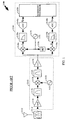
- FIG. 1 A block diagram of an exemplary super-heterodyne receiver 2100 of the prior art which is used for quadrature demodulation of QSPK, OQPSK, and QAM signal is illustrated in FIG. 1 .
- Receiver 2100 can be used at the base station or the remote station.
- the transmitted RF signal is received by antenna 2112 , routed through duplexer 2114 , and provided to front end 2102 .
- amplifier (AMP) 2116 Within front end 2102 , amplifier (AMP) 2116 amplifies the signal and provides the signal to bandpass filter 2118 which filters the signal to remove undesired signals.
- undesired signals comprise noise, spurious signals, undesirable images, interference, and jammers.
- the filtered RF signal is provided to mixer 2120 which downconverts the signal to a fixed intermediate frequency (IF) with the sinusoid from local oscillator (LO1) 2122 .
- the IF signal from mixer 2120 is filtered by bandpass filter 2124 and amplified by automatic gain control (AGC) amplifier 2126 to produce the required signal amplitude at the input of analog-to-digital-converters (ADCs) 2140 .
- ADCs analog-to-digital-converters
- the gain controlled signal is provided to demodulator 2104 .
- two mixers 2128a and 2128b downconvert the signal into the baseband I and Q signals with the sinusoid provided by local oscillator (LO2) 2134 and phase shifter 2136 , respectively.
- the baseband I and Q signals are provided to lowpass filters 2130a and 2130b , respectively, which provide match filtering, adjacent channel rejection, and/or anti-alias filtering of the baseband signals.
- the filtered signals are provided to ADCs 2140a and 2140b which sample the signals to produce the digitized baseband samples.
- the samples are provided to baseband processor 2150 for further processing (e.g. error detection, error correction, and decompression) to produce reconstructed estimates of the transmitted data.
- the first frequency downconversion with mixer 2120 allows receiver 2100 to downconvert signals at various RF frequencies to a fixed IF frequency where more signal processing can be performed.
- the fixed IF frequency allows bandpass filter 2124 to be implemented as a fixed bandpass filter, such as a surface acoustic wave (SAW) filter, to remove undesired signals from the IF signal. Removal of undesired signals is important since these signals can fold into the signal band (e.g. the band where the input signal is present) at the second frequency downconversion stage.
- the undesired signals can significantly increase the amplitude of the signal into various active components, such as the amplifiers and mixers, which can cause higher level of intermodulation products from the non-linearity in the active components. Undesired signals and intermodulation products can cause degradation in the performance of the communication system.
- the quadrature demodulator of the prior art has several major drawbacks.
- the required filtering by bandpass filter 2124 and/or lowpass filters 2130 can be complex. These filters may require a flat passband, high attenuation in the stopband, and sharp roll-off in the transition band.
- These filters are implemented with analog circuits. Component tolerance of analog circuits is difficult to maintain and can cause distortion in the frequency response of these filters. The performance of receiver 2100 can be degraded as the result of the distortion.
- quadrature balance is difficult to maintain over many production units because of component tolerance in phase splitter 2136 , mixers 2128 , lowpass filter 2130 , and ADCs 2140 .
- Any mismatch in the two signal paths results in quadrature imbalance and degradation in the performance of receiver 2100 .
- Path mismatch results in cross-talk of the I signal onto the Q signal, and vice versa.
- the cross-talk signal behaves as additive noise in the desired signal and results in poor detection of the desired signal.
- the prior art receiver architecture has DC offset because the analog filters are at baseband.
- ADCs 2140 can cause degradation in the performance of receiver 2100 for various reasons described below.
- one or more ADCs are required to convert an analog waveform in continuous time into discrete samples at evenly spaced time intervals.
- Some important performance parameters of an ADC include dynamic range, linearity, and DC offset. Each of these parameters can affect the performance of the communication system. Dynamic range can affect the bit-error-rate (BER) performance of the receiver because the noise from the ADC degrades the ability of the ADC to properly detect the input signal. Linearity relates to the difference between an actual transfer curve (e.g. digital output versus analog input) and the ideal transfer curve. Good linearity is more difficult to obtain as the number of bits in the ADC increases. Poor linearity can degrade the error detection/correction process. And DC offset can degrade the performance of the phase locked loop in the receiver and of the error correcting decoder, such as the Viterbi decoder.
- BER bit-error-rate
- flash ADCs or successive approximation ADCs are used to sample the baseband signals.
- the comparison signals are compared against L-1 reference voltages, which are generated by a second resistive ladder, by L-1 comparators.
- Flash ADCs are bulky and consume high power because L-1 comparators and 2L resistors are required. Flash ADCs can have poor linearity and poor DC offset characteristics if the resistors in the resistive ladder are not matched. However, flash ADCs are popular because of their high operating speed.
- Successive approximation ADCs are also popular for communication systems. These ADCs minimize complexity by performing approximations of the input signal over two or more stages. However, these ADCs can also exhibit poor linearity and poor DC offset characteristics similar to those of the flash ADCs. Thus, flash ADCs and successive approximation ADCs are not ideal candidates for use in many communication applications.
- Sigma delta analog-to-digital converters have better performance than flash and successive approximation ADCs because of the inherent architecture of the ⁇ ADC.
- ⁇ ADC performs analog-to-digital conversion of the input signal by making successive one-bit approximations of the input signal at a sampling frequency which is many times higher than the bandwidth of the input signal.
- the output samples comprise the input signal and the quantization noise.
- the ⁇ ADC can be designed such that the quantization noise in the signal band (e.g. the band where the signal is present) is pushed to out-of-band frequency (or noise shaped) where filtering is more easily performed.
- the out-of-band quantization noise is normally not an additional concern because filtering is typically provided in communication devices to remove undesired signals, such as jammers.
- ⁇ ADC can provide high dynamic range, good linearity, and low DC offset because of the inherent structure of the ⁇ ADC.
- high dynamic range can be obtained by selecting a sufficient oversampling ratio (OSR) and the proper noise shaping filter characteristic.
- OSR oversampling ratio
- bandpass sampling the oversampling ratio is defined as the sampling frequency divided by the two-sided bandwidth of the input.
- good linearity can be obtained because of the simple one-bit quantizer within the ⁇ ADC.
- DC offset is still present but is located away from the desired signal.
- ⁇ ADCs have been traditionally limited to applications where the input signal is a low bandwidth signal, such as audio application.
- ⁇ ADCs can be implemented to operate at high speed.
- High speed bandpass and baseband ⁇ ADC designs and implementations are disclosed in detail in copending U.S. Patent Application Serial No. 08/928,874 , entitled “BANDPASS SIGMA-DELTA ANALOG-TO-DIGITAL CONVERTER", filed September 12, 1997, assigned to the assignee of the present invention.
- WO 93/07679 A relates to a NMR receiver utilizing the Sigma-Delta modulation method implemented in the analog-to-digital converter device to enable the use of analog anti-aliasing filters that have a wider bandwidth.
- the analog filters do not induce phase distorsion of the signal in the operating frequency and thus eliminates the need for first order phase correction by the digital signal processor.
- the digital decimation filter contained within the analog-to-digital converter device acts as a digital lowpass filter.
- a receiver for demodulating an RF signal as set forth in claim 1 and claim 23, is provided.
- Embodiments of the present invention are claimed in the dependent claims.
- the present invention is a novel and improved receiver which comprises a sigma-delta analog-to-digital converter ( ⁇ ADC).
- the present invention can be utilized in one of four configurations, as a subsampling bandpass receiver, a subsampling baseband receiver, a Nyquist sampling bandpass receiver, or a Nyquist sampling baseband receiver.
- the sampling frequency is less than twice the center frequency of the input signal to the ⁇ ADC.
- Nyquist sampling ⁇ receivers the sampling frequency is at least twice the highest frequency of the input signal to the ⁇ ADC.
- the center frequency of the output signal from the ⁇ ADC is approximately zero or DC.
- the center frequency of the output signal from the ⁇ ADC is greater than zero.
- the center frequency of the input signal into the ⁇ ADC is placed such that the center frequency of the output signal from the ⁇ ADC is approximately 0.25•f s , where f s is the sampling frequency of the ⁇ ADC.
- This 0.25•f s center frequency simplifies the inphase and quadrature separation and provides the maximum separation between the aliases, but is not a necessary requirement.
- the sampling frequency can further be selected based on the bandwidth of the input signal to simplify the design of the digital circuits used to process the output samples from the ⁇ ADC.
- the center frequency of the input signal can be selected based on the sampling frequency and the bandwidth of the input signal.
- the use of a subsampling ⁇ ADC within the receiver provides many benefits including (1) elimination of an analog frequency downconversion stage which is provided for by subsampling of the input signal and the aliasing property of sampling, (2) reduction of the analog filtering requirements by clocking the ⁇ ADC at a high oversampling ratio and designing the ⁇ ADC with additional bits of resolution which can be used to handle undesired signals, (3) improvement in reliability and increase in flexibility by the use of digital demodulation for the output samples from the ⁇ ADC, (4) elimination of quadrature imbalance by designing the digital circuits to have the requisite quadrature balance, (5) improvement in dynamic range, linearity, and DC offset by the use of a ⁇ ADC, and (6) reduction in power consumption.
- the use of the Nyquist sampling ⁇ ADC provides many benefits such as improved dynamic range, increased linearity, reduced DC offset, and minimum power consumption.
- the present invention utilizes the superior performance of a high speed sigma-delta analog-to-digital converter ( ⁇ ADC) to perform the required analog-to-digital conversion of an analog waveform.
- exemplary applications include CDMA communication systems and HDTV signals.
- the input signal is centered at an intermediate frequency (IF) instead of baseband.
- IF intermediate frequency
- subsampling denotes that the sampling frequency of the ⁇ ADC is less than twice the center frequency of the input signal into the ⁇ ADC. Sampling at of a signal located at an IF frequency allows for the elimination of a frequency downconversion stage in the receiver, thus simplifying the hardware design and improving reliability.
- the noise shaper within the ⁇ ADC can be designed such that the quantization noise around the signal band is pushed out-of-band (or noise shaped) where filtering is more easily performed.
- the ⁇ ADC can be a bandpass ⁇ ADC or a baseband ⁇ ADC, depending on the application and the requirements.
- baseband sampling or baseband ⁇ ADC
- bandpass sampling or bandpass ⁇ ADC
- the use of ⁇ ADC provides many advantages over conventional (e.g.
- the input signal can be at baseband or an IF frequency and a baseband or a bandpass ⁇ ADC can be used to sample the input signal, respectively.
- Nyquist sampling denotes that the sampling frequency of the ⁇ ADC is at least twice the highest frequency of the input signal into the ⁇ ADC.
- the ⁇ ADC samples an analog waveform in continuous time to provide discrete samples at evenly spaced intervals.
- the ADC output Y(z) comprises the input signal X(z) which is shaped by the signal transfer function STF(z) plus the quantization noise E(z) which is shaped by the noise transfer function NTF(z).
- the signal transfer function STF(z) is typically designed such that, within the desired degree of required accuracy, it is frequency independent in the band of interest.
- STF(z) can be an allpass function comprising a fixed gain (A 1 ) and delay elements (z -1 ), such as A 1 •z -k .
- the quantization noise E(z) can be shaped by the noise transfer function NTF(z) such that the quantization noise in the signal band is pushed out-of-band where filtering is more easily performed.
- the characteristics of the noise transfer function NTF(z) is selected based on the application for which the ADC is used and is designed to provide the required performance.
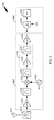
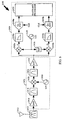
- Receiver 2200 can be used to demodulate BPSK, QPSK, OQPSK, QAM, and other digital and analog modulation formats.
- the transmitted signal is received by antenna 2212 , routed through duplexer 2214 , and provided to front end 2202 .
- amplifier (AMP) 2216 amplifies the signal and provides the amplified signal to bandpass filter 2218 which filters the signal to remove undesired signals.
- bandpass filter 2218 is a surface acoustic wave (SAW) filter, the implementation of which is known in the art.
- SAW surface acoustic wave
- the filtered signal is provided to mixer 2220 which downconverts the signal with the sinusoid from local oscillator (LO1) 2222 .
- the IF signal from mixer 2220 is provided to bandpass filter 2224 which further filters the signal.
- bandpass filter 2224 is another SAW filter which removes undesired signals which will alias into the band of interest and reduces the required dynamic range by filtering the jammers.
- the filtered signal from bandpass filter 2224 is provided to IF processor 2230 .
- the filtered signal is amplified by amplifier 2232 and filtered by bandpass filter 2234 to further remove undesired signals.
- Bandpass filter 2234 is included to provide further anti-alias filtering.
- the filtered signal is provided to buffer (BUF) 2236 which provides gain and/or buffering of the signal.
- the gain and filtering provided by IF processor 2230 is not necessary. In this case, the signal from bandpass filter 2224 is provided directly to buffer 2236 .
- the buffered signal is provided to demodulator 2204 .
- ⁇ ADC 2240 samples the buffered signal at a high sampling frequency determined by the CLK signal and provides the samples to digital signal processor (DSP) 2250 .
- DSP digital signal processor
- Receiver 2200 comprises the basic functionalities required by most receivers. However, the arrangement of amplifiers 2216 and 2232 , bandpass filters 2218, 2224 , and 2234 , and mixer 2220 can be reordered to optimize the performance of receiver 2200 for specific applications. For example, bandpass filter 2218 can be interposed between duplexer 2214 and amplifier 2216 to filter out undesired signals before the first amplifier stage. Amplifier 2216 can replaced with a low noise amplifier (LNA) or an automatic gain control (AGC) amplifier to provide the required gain and AGC control. Additional frequency downconversion stages can also be added within receiver 2200 as required. Different arrangements of the functionalities shown herein can be contemplated and are within the scope of the present invention. Furthermore, other arrangements of the functionalities shown herein in combination with other receiver functionalities which are known in the art can also be contemplated and are within the scope of the present invention.
- LNA low noise amplifier
- AGC automatic gain control
- Receiver 2300 provides the benefits of subsampling ⁇ receiver 2200 in addition to the benefits of a programmable linear receiver as disclosed in copending U.S. Patent Application Serial No. 08/928,874 .
- the transmitted RF signal is received by antenna 2312 , routed through duplexer 2314 , and provided to attenuator 2316 .
- Attenuator 2316 attenuates the RF signal to provide a signal at the required amplitude and provides the attenuated signal to front end 2302 .
- the attenuated signal is provided to pad 2322a and low noise amplifier (LNA) 2320a .
- LNA low noise amplifier
- LNA 2320a amplifies the RF signal and provides the amplified signal to bandpass filter 2326 .
- Pad 2322a provides a predetermined level of attenuation and connects in series with switch 2324a .
- Switch 2324a provides a bypass route around LNA 2320a when the gain of LNA 2320a is not required.
- Bandpass filter 2326 filters the signal to remove undesired signals which can cause intermodulation products in the subsequent signal processing stages.
- the filtered signal is provided to pad 2322b and low noise amplifier (LNA) 2320b .
- LNA 2320b amplifies the filtered signal and provides the signal to mixer 2330 .
- Pad 2322b provides a predetermined level of attenuation and connects in series with switch 2324b .
- Switch 2324b provides a bypass route around LNA 2320b when the gain of LNA 2320b is not required.
- Mixer 2330 downconverts the signal to an IF frequency with the sinusoid from local oscillator (LO1) 2328.
- the IF signal is provided to bandpass filter 2332 which filters out undesired signals and out-of-band downconversion products.
- the filtered IF signal is provided to amplifier (AMP) 2334 which amplifies the signal.
- the amplified IF signal is provided to demodulator 2304 which demodulates the signal in accordance with the modulation format used at the transmitter. Demodulator 2304 is identical to demodulator 2204 (see FIG. 2 ) which is described below.
- amplifier 2334 which can be implemented as a voltage control amplifier (VGA), digital signal processor (DSP) 2350 within demodulator 2304 , the reference voltage within ⁇ ADC 2340 , or combinations of the above.
- VGA voltage control amplifier
- DSP digital signal processor
- a bandpass ⁇ ADC For applications wherein quadrature demodulation is required, such as QPSK, OQPSK, and QAM, a bandpass ⁇ ADC is utilized.
- the bandpass ⁇ ADC can be designed and implemented in the manner described in copending U.S. Patent Application Serial No. 08/928,874 .
- the bandpass ⁇ ADC samples the IF signal from amplifier 2334 and provides the IF samples to digital signal processor 2250 .
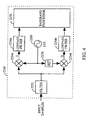
- FIG. 4 An exemplary block diagram of digital signal processor 2250 used for quadrature demodulation is illustrated in FIG. 4 .
- the quantized IF samples from ⁇ ADC 2240 are provided to filter 2252 which filters and decimates the IF samples.
- the filtered samples are provided to multipliers 2254a and 2254b which downconvert the filtered samples to the baseband I and Q samples with the inphase and quadrature sinusoids from local oscillator (LO2) 2560 and phase shifter 2258, respectively.
- LO2 local oscillator
- Phase shifter 2258 provides 90° of phase shift for the quadrature sinusoid.
- the baseband I and Q samples are provided to lowpass filters 2256a and 225b , respectively, which filters the samples to provide the I and Q data.
- the I and Q data are provided to baseband processor 2270 which performs additional signal processing, such as error detection/correction and decompression.
- filter 2252 and/or lowpass filters 2256 also provide scaling of the samples to enable digital signal processor 2250 to provide baseband data at various amplitude.
- Other implementations of digital signal processor 2250 can be designed to performed quadrature demodulation and are within the scope of the present invention.
- a baseband ⁇ ADC can be used for applications wherein quadrature demodulation is not required, such as BPSK and FM.
- the baseband ⁇ ADC can be designed and implemented in the manner described in copending U.S. Patent Application Serial No. 08/928,874 .
- Subsampling ⁇ receivers such as receivers 2200 and 2300 , have many advantages over the super-heterodyne receiver 2100 of the prior art.
- the second analog frequency downconversion stage e.g. mixers 2128 in FIG. 1
- subsampling ⁇ receivers require less stringent anti-alias analog filtering because of the high oversampling ratio and high dynamic range of the ⁇ ADC. These characteristics allows the bulk of the filtering function to be moved to the subsequent digital filters.
- the digital signal processing after the ⁇ ADC can be performed with the required precision and with improved reliability over the analog processing of the prior art.
- ⁇ ADC of the present invention can provide improved dynamic range, linearity, and DC offset over the conventional ADCs used in the prior art.
- the first major advantage of the subsampling ⁇ receivers of the present invention is the elimination of an analog frequency downconversion stage.
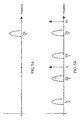
- the diagrams of the frequency spectrum of the IF input and the frequency spectrum of the IF samples from the ⁇ ADC for a subsampling bandpass ⁇ receiver are illustrated in FIGS. 5A-5B , respectively.
- the center frequency of the IF signal can be controlled by changing the frequency of the local oscillator within the front end (e.g. local oscillator 2222 in FIG. 2 ).
- the IF signal aliases and images of the IF signal appear at 0.25•f s , 0.75•f s , 1.25•f s , 1.75•f s and so on (see FIG. 5B ).
- Undersampling denotes that the sampling frequency is less than twice the highest frequency of the IF signal.
- the IF signal at 1.75•f s is effectively downconverted to 0.25•f s without the use of an analog downconversion stage.
- the signal at 0.25•f s is subsequently processed by the digital signal processor.
- the ⁇ ADC is a bandpass ⁇ ADC which shapes the quantization noise in the manner as disclosed in copending U.S. Patent Application Serial No. 08/928,874 .
- the quantization noise around 0.25•f s is pushed to DC and 0.50•f s where filtering of the quantization noise is more easily performed.
- the center frequency of the IF signal is selected such that an image appears at 0.25•f s , the frequency where the quantization noise is minimal.
- the samples from filter 2252 is downconverted to baseband by multipliers 2254a and 2254b with the inphase and quadrature sinusoids from local oscillator 2260 and phase splitter 2258 , respectively.
- the frequency downconversion stage can be made trivial.
- the samples from the ⁇ ADC are provided to filter 2252 which filters the IF samples and decimates by N to produce decimated samples at the decimated frequency f d .
- multipliers 2254a and 2254b can be performed by multiplying the decimated samples from filter 2252 with the sequences (1, 0, -1, 0, 1, 0, -1,...) and (0, 1, 0, -1, 0, 1, 0,...), respectively.
- multipliers 2254a and 2254b can be implemented with simple digital circuits.
- the subsampling ⁇ receiver of the present invention in used to demodulate CDMA signals having a two-sided bandwidth of 1.2288 MHz.
- the decimated frequency f d is selected to be chipx8 (9.83 MHz), or eight times the two-sided bandwidth of the CDMA signal, for ease implementing the quadrature downconversion stage and the subsequent signal processing stages.
- sampling and IF frequencies can also be used and are within the scope of the present invention.
- the ratio of the sampling frequency over the decimated frequency is 6.77 (66.6 MHz/9.83 MHz) which is not an integer.
- a data rate converter is used to resample the IF samples at f s into converted samples at a converted frequency f c .
- the data rate converter can be implemented in a manner known in the art, such as a linear interpolator or a quadratic interpolator as described in detail in 08/928,874. In some applications wherein the frequency plan allows for sampling at a sampling frequency which is p times the decimated frequency f d , where p is an integer, the data rate converter is not required.
- the second major advantage of subsampling ⁇ receivers is less stringent requirements on the analog filters.
- Within the front end of the subsampling ⁇ receivers only simple anti-alias filtering is necessary to remove undesired signals from the output signal from the first mixer (e.g. mixer 2220 ) before sampling by ⁇ ADC.
- the stringent analog match filters which are required in receiver 2100 are implemented with digital filters within the digital signal processor.
- Stringent analog filters may also be needed in receiver 2100 to suppress undesired signals.
- undesired signals of large amplitude e.g., comprising jammers
- the jammers can be much higher in amplitude than the desired signal.
- sharp analog filters are required to suppress the jammers to a smaller amplitude so that the ADCs are not clipped, since clipping of the ADCs causes intermodulation products which degrade the desired signal.
- the ⁇ ADC in the present invention can be designed with additional bits of resolution which can be used to quantize the jammers without clipping the ⁇ ADC. The additional bits enable the ⁇ ADC to tolerate higher amplitude jammers, thereby relaxing the requirements of the analog filters before the ⁇ ADC.
- filter 2252 and lowpass filters 2256a and 2256b can be designed to provide the required match filtering of the input signal which is typically required by a demodulator for optimal performance.
- Implementation of the filters with digital filters such as finite impulse response (FIR) filters, infinite impulse response (IIR) filters, or polyphase filters, allows for high performance and increased reliability.
- the digital filters can also be designed to achieve the required precision while minimizing circuit complexity.
- Digital filters can also provide improved performance since the frequency response of the digital filters is identical for all units produced. Consistency is important for receivers which are produced in high quantity.
- the digital filters can be designed to meet any required specifications (e.g. any required frequency response).
- the digital filters can also be designed with the flexibility to provide the optimal frequency response based on the requirements of the application.
- the FIR filters can be designed with filter tap coefficients which can be loaded from a controller. The frequency response of the FIR filters can then be dynamically varied for different operating modes.
- the digital filters can be designed in stages, and some stages can be bypassed when not required to minimize power consumption.
- Digital quadrature demodulation can be implemented with digital circuits which can be integrated into one or few integrated circuits (ICs) to minimize component count, decrease cost, and improve reliability.
- digital circuits can be easily tested during the manufacturing phase and/or the operational phase.
- quadrature demodulation is implemented with analog circuits. Poor component tolerance in analog circuits can result in the receiver not meeting the required performance specifications.
- analog circuits comprise many components which can degrade the reliability of the receiver and increase cost.
- the analog circuits of the prior art need to be redesigned for each of multiples standards, e.g" to meet the IS-95 standard, the Korean standard, and the Japanese standard,
- the fourth major advantage of the subsampling ⁇ receiver is the elimination of quadrature mismatch.
- the quadrature imbalance found in analog quadrature demodulator is eliminated.
- multipliers 2254 and lowpass filters 2256 are designed to be identical.
- the inphase and quadrature sinusoids from local oscillator 2260 and phase shifter 2258 , respectively are generated from different values (e.g. 1, 0, or -1) associated with the same clock signal and have no phase error.
- the two signal paths are matched and in exact quadrature to one another.
- any mismatch in the two signal paths e.g. error in phase splitter 2136 and/or mismatch in mixers 2128 , lowpass filters 2130 , and ADCs 2140 ) results in cross-talk of the I signal onto the Q signal, and vice versa.
- the cross-talk results in degradation of the BER performance of the analog quadrature demodulator.
- the fifth major advantage of the subsampling ⁇ receiver is that the ⁇ ADC can be designed to provide improved dynamic range, linearity, and DC offset over that of the conventional (e.g. flash and successive approximation) ADCs used in the prior art.
- Noise shaping of the quantization noise by the ⁇ ADC provides improved dynamic range over conventional ADCs since the amount of quantization noise in the signal band is reduced.
- the quantization noise is white across the output spectrum from DC to the sampling frequency.
- the quantization noise is minimal in the signal band through proper design of the noise shaper within the ⁇ ADC.
- the noise shaper can be designed to match the characteristics of the IF signal and the performance requirements.
- the improved dynamic range offered by the ⁇ ADC also results from the high oversampling of the input signal.
- the output of the ⁇ ADC can be 1-bit or m-bits, depending on whether a single-loop architecture or a MASH (Multi-stAge noise SHaper) architecture is used and whether a single-bit or a multi-bit quantizer is used.
- the sampling frequency is selected to be much higher than the signal bandwidth. Therefore, the quantization noise is spread over the a wider spectrum, from DC to the sampling frequency.
- the ⁇ ADC can have 12 or more bits of resolution.
- the resolution can be designed by proper selection of the oversampling ratio, the noise shaper, and the order of the ⁇ ADC.
- the IF signal into the ⁇ ADC typically comprises the desired signal plus undesired signals which can comprise jammers.
- the amplitude of the jammers can be much larger than the amplitude of the desired signal.
- the IF signal is scaled to fit within the full-scale input of the ADC. As the amplitude of the jammers increases, the desired signal becomes a smaller percentage of the input IF signal. More bits of resolution is required from the ADC to adequately quantize the desired signal.
- the amplitude of the jammers is minimized by filtering the analog signal with complex filters before sampling by the ADCs. Since the jammers can be located close to the signal band (e.g. 900 KHz away from the center frequency of the CDMA signal), sharp roll-off filters such as SAW filters and high order elliptical filters are required to minimize the amplitude of the jammers. These sharp roll-off filters can be complex to design, difficult to manufacture, and costly.
- the additional number of bits of resolution provided by the ⁇ ADC of the present invention corresponds to higher dynamic range and allows for jammers of larger amplitude in the IF signal without degradation of the desired signal.
- the higher resolution allows the ⁇ ADC to properly quantize the desired signal even if it is only a small fraction of the input IF signal.
- only four bits of resolution are required for proper demodulation of the desired signal.
- the remaining eight bits can be used to handle jammers and/or to provide gain control.
- the ⁇ ADC of the present invention also provides improved linearity and DC offset characteristics over the conventional ADCs of the prior art.
- linearity is dependent on the matching of the resistors in the two resistive ladders used to divide the input signal and the reference voltage, as described above.
- the number of resistors in a ladder is 2 m , where m in the number of bits in the ADC. As m increases, linearity is more difficult to maintain because of the number of resistors which need to be matched. In contrast, for ⁇ ADC, linearity is more easily achieved because a single-bit quantizer can be used. As long as the high and low feedback voltages within the ⁇ ADC are maintained at a constant level, linearity is maintained.
- Non-linearity can degrade the performance of the receiver, such as the bit-error-rate (BER) or the frame-error-rate (FER).
- Non-linearity can also degrade the performance of the multiple loops within the receiver, such as the carrier-tracking loop and the bit-timing loop.
- the carrier-tracking-loop tracks the frequency/phase of the input RF signal and bit-timing-loop tracks the symbol rate of the input signal.
- Non-linearity can also affect the measurement of the signal level which is used in the automatic gain control (AGC) circuit and the bias control circuit used to improve the input-referred third order intermodulation product (IIP3) performance.
- AGC automatic gain control
- IIP3 input-referred third order intermodulation product
- the ⁇ ADC also has improved DC offset characteristics over the conventional ADC of the prior art.
- DC offset is improved because the analog filters of the prior art that amplifies DC is no longer present in the present invention.
- bandpass ⁇ ADC DC offset is not a concern because this spectral component is out-of-band. Any DC offset can be filtered out and contributes little to the output samples.
- DC offset is particularly important for digital communication system since this parameter can degrade the BER performance and the performance of the phase locked loops within the receiver.
- DC offset skews the quantization of the ADC output samples and can result in erroneous detection of the input signal.
- DC offset can also degrade the performance of the Viterbi decoding process, which is commonly used in digital communication systems.
- DC offset affects the performance of the carrier-tracking and bit-timing loops.
- DC offset introduces a DC bias into the loops which degrades the acquisition performance of the loops. The DC bias also stresses the loops, thereby degrading the tracking performance of the loops.
- DC offset is an important design and manufacturing consideration which is addressed by one or a combination of measures.
- the DC offset of each ADC can be carefully screened to specified limits.
- special compensation loops can be designed to estimate and track out the DC offset of each ADC.
- the design of the ⁇ ADC as described in copending U.S. Patent Application Serial No. 08/928,874 provides additional benefits when used within the receiver of the present invention.
- the ⁇ ADC can be reconfigured during operation such that portions of the ⁇ ADC can be turned OFF to conserve power when high performance is not required.
- the ⁇ ADC can be implemented as a two-loop MASH architecture and one loop can be turned OFF when high dynamic range is not required.
- the ⁇ ADC Another benefit provided by the ⁇ ADC is the ease of interface between the ⁇ ADC and other circuitry within the receiver.
- the ⁇ ADC only outputs one or few bits at each sampling clock cycle even though the ⁇ ADC may have more bits of resolution.
- the ⁇ ADC has few input/output (I/O) pins.
- I/O input/output
- only one ⁇ ADC is required for subsampling ⁇ receivers. Fewer ADC and I/O pins simplify the routing between the ⁇ ADC and other circuits within the receiver.
- one I/O pin is typically required for each bit of resolution.
- two conventional ADCs are required for a quadrature demodulator as shown in FIG. 1 . The high number of ADCs and I/O pins can make the layout and routing more difficult.
- Receivers 2200 and 2300 are two exemplary receiver architectures which support subsampling ⁇ analog-to-digital conversion of the IF signal.
- Other receiver architectures can be design to provide the necessary front end processing based on the requirements of the application for which the receiver is used.
- other digital signal processors can be designed to perform demodulation of the IF samples.
- different receiver architectures which comprise a subsampling ⁇ ADC are within the scope of the present invention.
- the receiver comprises a subsampling ⁇ ADC.
- This architecture provides many benefits as described above.
- the receiver comprises a Nyquist sampling ⁇ ADC.
- This architecture provides many of the benefits of the ⁇ ADC, specifically high dynamic range, improved linearity, low DC offset, and minimal power consumption.
- the sampling frequency is at least twice the highest frequency of the input signal into the ADC so that aliasing is avoided rather than utilized.
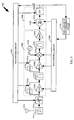
- Receiver 2400 can be used to demodulate BPSK, QPSK, OQPSK, QAM, and digital and analog modulation formats.
- the transmitted signal is received by antenna 2412 , routed through duplexer 2414 , and provided to front end 2402 .
- amplifier (AMP) 2416 amplifies the signal and provides the amplified signal to bandpass filter 2418 which filters the signal to remove undesired signals.
- bandpass filter 2418 is a surface acoustic wave (SAW) filter.
- SAW surface acoustic wave
- the filtered signal is provided to mixer 2420 which downconverts the signal with the sinusoid from local oscillator (LO1) 2422.
- the IF signal from mixer 2420 is filtered by bandpass filter 2424 and amplified by automatic gain control (AGC) amplifier 2426 to produce the required signal amplitude at the input of ⁇ ADCs 2440 .
- bandpass filter 2424 is also a SAW filter.
- the AGCed signal is provided to demodulator 2404 .
- Demodulator 2404 provides quadrature demodulation utilizing Nyquist sampling baseband ⁇ ADCs.
- two mixers 2428a and 2428b downconvert the signal into the baseband I and Q signals with the sinusoid provided by local oscillator (LO2) 2434 and phase shifter 2436 , respectively.
- the baseband I and Q signals are provided to lowpass filters 2430a and 2430b , respectively, which provide match filtering and/or anti-alias filtering of the baseband signals.
- the filtered signals are provided to ⁇ ADCs 2440a and 2440b which sample the signals to produce the digitized baseband samples.
- the samples are provided to baseband processor 2450 for further processing (e.g. error detection and/or correction, decompression).
- ⁇ ADCs 2440 are Nyquist sampling baseband ⁇ ADC which can be implemented in the manner disclosed in copending U.S. Patent Application Serial No. 08/928,874 .
- the baseband ⁇ ADC pushes the quantization noise around DC to higher frequency where filtering is more easily performed.
- Nyquist sampling ⁇ receiver can be designed to perform digital quadrature demodulation similar to subsampling ⁇ receivers 2200 and 2300 .
- subsampling ⁇ receivers 2200 and 2300 are designed such that the center frequency of the IF signal into the bandpass ⁇ ADC is at an IF frequency.
- the IF frequency is selected to be 0.25•f s .
- This IF frequency can be obtained by adjusting the frequency of the first local oscillator (e.g. LO1 2222 ) or by a second frequency downconversion stage interposed between the first frequency downconversion stage (e.g. mixer 2200 ) and the bandpass ⁇ ADC.
Landscapes
- Engineering & Computer Science (AREA)
- Computer Networks & Wireless Communication (AREA)
- Signal Processing (AREA)
- Power Engineering (AREA)
- Compression, Expansion, Code Conversion, And Decoders (AREA)
- Analogue/Digital Conversion (AREA)
- Transmission Systems Not Characterized By The Medium Used For Transmission (AREA)
Applications Claiming Priority (3)
| Application Number | Priority Date | Filing Date | Title |
|---|---|---|---|
| US08/987,306 US6005506A (en) | 1997-12-09 | 1997-12-09 | Receiver with sigma-delta analog-to-digital converter for sampling a received signal |
| US987306 | 1997-12-09 | ||
| PCT/US1998/026051 WO1999030428A1 (en) | 1997-12-09 | 1998-12-08 | Receiver with sigma-delta analog-to-digital converter |
Publications (2)
| Publication Number | Publication Date |
|---|---|
| EP1040587A1 EP1040587A1 (en) | 2000-10-04 |
| EP1040587B1 true EP1040587B1 (en) | 2008-02-27 |
Family
ID=25533178
Family Applications (1)
| Application Number | Title | Priority Date | Filing Date |
|---|---|---|---|
| EP98962004A Expired - Lifetime EP1040587B1 (en) | 1997-12-09 | 1998-12-08 | Receiver with sigma-delta analog-to-digital converter |
Country Status (17)
| Country | Link |
|---|---|
| US (1) | US6005506A (es) |
| EP (1) | EP1040587B1 (es) |
| JP (1) | JP2001526487A (es) |
| KR (1) | KR100712412B1 (es) |
| CN (1) | CN1178401C (es) |
| AR (1) | AR017818A1 (es) |
| AU (1) | AU746148B2 (es) |
| BR (1) | BR9813414A (es) |
| CA (1) | CA2313139C (es) |
| DE (1) | DE69839192T2 (es) |
| DK (1) | DK1040587T3 (es) |
| ES (1) | ES2301217T3 (es) |
| IL (1) | IL136403A0 (es) |
| MX (1) | MXPA00005773A (es) |
| MY (1) | MY114831A (es) |
| WO (1) | WO1999030428A1 (es) |
| ZA (1) | ZA9811125B (es) |
Families Citing this family (140)
| Publication number | Priority date | Publication date | Assignee | Title |
|---|---|---|---|---|
| US6751272B1 (en) * | 1998-02-11 | 2004-06-15 | 3Com Corporation | Dynamic adjustment to preserve signal-to-noise ratio in a quadrature detector system |
| US6185248B1 (en) * | 1998-03-12 | 2001-02-06 | Northrop Grumman Corporation | Wideband digital microwave receiver |
| US6792267B1 (en) * | 1998-05-29 | 2004-09-14 | Ericsson Inc. | Systems and methods for uplinking downsampled radiotelephone signals from cellular radiotelephone base stations to a cellular radio exchange |
| GB2338853B (en) * | 1998-06-18 | 2002-11-06 | Ericsson Telefon Ab L M | Radio receiver |
| US6459743B1 (en) * | 1998-08-07 | 2002-10-01 | Telefonaktiebolaget Lm Ericsson (Publ) | Digital reception with radio frequency sampling |
| US7515896B1 (en) | 1998-10-21 | 2009-04-07 | Parkervision, Inc. | Method and system for down-converting an electromagnetic signal, and transforms for same, and aperture relationships |
| US6061551A (en) | 1998-10-21 | 2000-05-09 | Parkervision, Inc. | Method and system for down-converting electromagnetic signals |
| US7039372B1 (en) | 1998-10-21 | 2006-05-02 | Parkervision, Inc. | Method and system for frequency up-conversion with modulation embodiments |
| US7236754B2 (en) | 1999-08-23 | 2007-06-26 | Parkervision, Inc. | Method and system for frequency up-conversion |
| US6370371B1 (en) | 1998-10-21 | 2002-04-09 | Parkervision, Inc. | Applications of universal frequency translation |
| CN1149734C (zh) * | 1998-10-22 | 2004-05-12 | 因芬尼昂技术股份公司 | 稳频的发射/接收电路装置 |
| EP1011191B1 (fr) * | 1998-12-08 | 2009-01-07 | Nxp B.V. | Dispositif de filtrage pour éliminer une composante continue |
| US7209725B1 (en) | 1999-01-22 | 2007-04-24 | Parkervision, Inc | Analog zero if FM decoder and embodiments thereof, such as the family radio service |
| US6748025B1 (en) * | 1999-02-02 | 2004-06-08 | Technoconcepts, Inc. | Direct conversion delta-sigma receiver |
| US6853690B1 (en) | 1999-04-16 | 2005-02-08 | Parkervision, Inc. | Method, system and apparatus for balanced frequency up-conversion of a baseband signal and 4-phase receiver and transceiver embodiments |
| US6879817B1 (en) | 1999-04-16 | 2005-04-12 | Parkervision, Inc. | DC offset, re-radiation, and I/Q solutions using universal frequency translation technology |
| US6304136B1 (en) * | 1999-03-03 | 2001-10-16 | Level One Communications, Inc. | Reduced noise sensitivity, high performance FM demodulator circuit and method |
| US6442154B1 (en) * | 1999-04-15 | 2002-08-27 | Ericsson Inc. | Method and apparatus for successive cancellation using multiple signal timings |
| US7110444B1 (en) | 1999-08-04 | 2006-09-19 | Parkervision, Inc. | Wireless local area network (WLAN) using universal frequency translation technology including multi-phase embodiments and circuit implementations |
| US7065162B1 (en) | 1999-04-16 | 2006-06-20 | Parkervision, Inc. | Method and system for down-converting an electromagnetic signal, and transforms for same |
| US7693230B2 (en) | 1999-04-16 | 2010-04-06 | Parkervision, Inc. | Apparatus and method of differential IQ frequency up-conversion |
| WO2000079706A1 (en) * | 1999-06-23 | 2000-12-28 | Ditrans Corporation | Direct conversion delta-sigma receiver |
| KR100404180B1 (ko) * | 1999-07-06 | 2003-11-03 | 엘지전자 주식회사 | 통신시스템에서의 기지국 신호 복조 장치 |
| WO2001010034A1 (en) * | 1999-07-28 | 2001-02-08 | Analog Devices, Inc. | Bandpass modulator |
| US8295406B1 (en) * | 1999-08-04 | 2012-10-23 | Parkervision, Inc. | Universal platform module for a plurality of communication protocols |
| DE19960559A1 (de) | 1999-12-15 | 2001-07-05 | Infineon Technologies Ag | Empfangsvorrichtung für winkelmodulierte Signale |
| EP1130785A3 (en) * | 2000-01-21 | 2004-03-17 | Texas Instruments Incorporated | Signal clipping circuit for switched capacitor sigma delta analog to digital converters |
| CA2442597C (en) | 2000-03-27 | 2011-11-01 | Transcept Opencell, Inc. | Multi-protocol distributed wireless system architecture |
| US7010286B2 (en) | 2000-04-14 | 2006-03-07 | Parkervision, Inc. | Apparatus, system, and method for down-converting and up-converting electromagnetic signals |
| GB2362279B (en) * | 2000-05-12 | 2004-12-29 | Global Silicon Ltd | Radio receiver |
| US7693236B2 (en) * | 2000-05-15 | 2010-04-06 | Texas Instruments Incorporated | If-to-baseband conversion for flexible frequency planning capability |
| US6621441B2 (en) * | 2000-05-15 | 2003-09-16 | Texas Instruments Incorporated | Attenuating undesired frequencies while sampling a communication signal |
| US6654594B1 (en) | 2000-05-30 | 2003-11-25 | Motorola, Inc. | Digitized automatic gain control system and methods for a controlled gain receiver |
| US6388526B1 (en) * | 2000-07-06 | 2002-05-14 | Lucent Technologies Inc. | Methods and apparatus for high performance reception of radio frequency communication signals |
| US6704545B1 (en) | 2000-07-19 | 2004-03-09 | Adc Telecommunications, Inc. | Point-to-multipoint digital radio frequency transport |
| JP2002043965A (ja) * | 2000-07-31 | 2002-02-08 | Pioneer Electronic Corp | 受信機 |
| DE10043744C1 (de) * | 2000-09-05 | 2002-07-11 | Infineon Technologies Ag | Empfangsschaltung für Mobilfunkempfänger mit automatischer Verstärkungssteuerung |
| DE10044456A1 (de) * | 2000-09-08 | 2002-04-04 | Infineon Technologies Ag | Empfängerschaltung, innsbesondere für den Mobilfunk |
| US6466150B1 (en) * | 2000-10-25 | 2002-10-15 | Qualcomm, Inc. | Polar analog-to-digital converter |
| GB0027503D0 (en) * | 2000-11-10 | 2000-12-27 | Koninkl Philips Electronics Nv | Radio receiver |
| US7454453B2 (en) | 2000-11-14 | 2008-11-18 | Parkervision, Inc. | Methods, systems, and computer program products for parallel correlation and applications thereof |
| US6452456B1 (en) | 2000-11-16 | 2002-09-17 | Texas Instruments Incorporated | Fast-setting, low power, jammer insensitive, biasing apparatus and method for single-ended circuits |
| US6639946B2 (en) * | 2000-12-01 | 2003-10-28 | International Business Machines Corporation | Sigma delta modulator with SAW filter |
| US6686860B2 (en) * | 2000-12-12 | 2004-02-03 | Massachusetts Institute Of Technology | Reconfigurable analog-to-digital converter |
| US7076225B2 (en) * | 2001-02-16 | 2006-07-11 | Qualcomm Incorporated | Variable gain selection in direct conversion receiver |
| WO2002069316A2 (en) * | 2001-02-27 | 2002-09-06 | Sikorsky Aircraft Corporation | System for computationally efficient active control of tonal sound or vibration |
| EP1371200B1 (en) * | 2001-03-01 | 2011-10-12 | Broadcom Corporation | Compensation of distortion due to channel and to receiver, in a parallel transmission system |
| US7248628B2 (en) * | 2001-03-02 | 2007-07-24 | Shaeffer Derek K | Method and apparatus for a programmable filter |
| US7079826B2 (en) * | 2001-03-16 | 2006-07-18 | Texas Instruments Incorporated | Digitally controlled analog RF filtering in subsampling communication receiver architecture |
| US7110732B2 (en) * | 2001-04-09 | 2006-09-19 | Texas Instruments Incorporated | Subsampling RF receiver architecture |
| US20040179628A1 (en) * | 2001-04-16 | 2004-09-16 | Abraham Haskin | Method and apparatus for digital data transmission and reception using synthetically generated frequency |
| KR100888300B1 (ko) | 2001-05-01 | 2009-03-11 | 마츠시타 커뮤니케이션 인더스트리얼 코포레이션 오브 유에스에이 | 언더 샘플링에 의한 주파수 변환 |
| US20040213333A1 (en) * | 2001-05-25 | 2004-10-28 | Kaibin Huang | Sigma-delta modulation code division multiple-access receiver |
| US6670901B2 (en) * | 2001-07-31 | 2003-12-30 | Motorola, Inc. | Dynamic range on demand receiver and method of varying same |
| US20030072393A1 (en) * | 2001-08-02 | 2003-04-17 | Jian Gu | Quadrature transceiver substantially free of adverse circuitry mismatch effects |
| US7415088B2 (en) * | 2001-08-31 | 2008-08-19 | Qualcomm Incorporated | Multi-standard baseband receiver |
| US6577258B2 (en) * | 2001-10-01 | 2003-06-10 | Nokia Corporation | Adaptive sigma-delta data converter for mobile terminals |
| WO2003032522A2 (en) * | 2001-10-08 | 2003-04-17 | Qinetiq Limited | Signal processing system and method for determininig antenna weights |
| CA2407242C (en) | 2001-10-10 | 2011-05-31 | David I. Havelock | Aggregate beamformer for use in a directional receiving array |
| US7072427B2 (en) | 2001-11-09 | 2006-07-04 | Parkervision, Inc. | Method and apparatus for reducing DC offsets in a communication system |
| US7149213B1 (en) | 2001-12-28 | 2006-12-12 | Advanced Micro Devices, Inc. | Wireless computer system with queue and scheduler |
| US7313104B1 (en) | 2001-12-28 | 2007-12-25 | Advanced Micro Devices, Inc. | Wireless computer system with latency masking |
| GB2384124B (en) * | 2002-01-10 | 2004-03-31 | Motorola Inc | Arrangement and method for radio receiver |
| US7088794B2 (en) * | 2002-02-19 | 2006-08-08 | The United States Of America As Represented By The Secretary Of The Navy | Automatic gain control for digitized RF signal processing |
| KR100674645B1 (ko) * | 2002-02-25 | 2007-01-25 | 매그나칩 반도체 유한회사 | 반도체 소자 제조 방법 |
| US8380143B2 (en) | 2002-05-01 | 2013-02-19 | Dali Systems Co. Ltd | Power amplifier time-delay invariant predistortion methods and apparatus |
| US8811917B2 (en) | 2002-05-01 | 2014-08-19 | Dali Systems Co. Ltd. | Digital hybrid mode power amplifier system |
| US6975846B2 (en) * | 2002-05-23 | 2005-12-13 | Intel Corporation | Method and circuit to reduce intermodulation distortion |
| US7460584B2 (en) | 2002-07-18 | 2008-12-02 | Parkervision, Inc. | Networking methods and systems |
| US7379883B2 (en) | 2002-07-18 | 2008-05-27 | Parkervision, Inc. | Networking methods and systems |
| US7398075B2 (en) * | 2002-08-09 | 2008-07-08 | Casio Computer Co., Ltd. | Radio wave reception device and radio wave clock |
| US7173980B2 (en) * | 2002-09-20 | 2007-02-06 | Ditrans Ip, Inc. | Complex-IF digital receiver |
| ATE544293T1 (de) * | 2002-10-07 | 2012-02-15 | Koninkl Philips Electronics Nv | Automatisches einstellen eines betriebszustands eines breitbandverstärkers |
| US8958789B2 (en) | 2002-12-03 | 2015-02-17 | Adc Telecommunications, Inc. | Distributed digital antenna system |
| US7187735B2 (en) * | 2003-01-28 | 2007-03-06 | Raytheon Company | Mixed technology MEMS/SiGe BiCMOS digitalized analog front end with direct RF sampling |
| US7555067B2 (en) * | 2003-03-13 | 2009-06-30 | Texas Instruments Incorporated | Method and apparatus for decoder input scaling based on interference estimation in CDMA |
| JP2005020591A (ja) * | 2003-06-27 | 2005-01-20 | Toshiba Corp | 可変利得増幅器、これを用いた光ピックアップ信号処理用および携帯無線端末送受信信号処理用lsi |
| ATE381155T1 (de) * | 2003-07-10 | 2007-12-15 | Nxp Bv | Empfänger zum empfang von frequenzsignalen unter verwendung von delta-sigma-modulatoren |
| US20050094584A1 (en) * | 2003-11-04 | 2005-05-05 | Advanced Micro Devices, Inc. | Architecture for a wireless local area network physical layer |
| US20050118977A1 (en) * | 2003-12-02 | 2005-06-02 | Drogi Serge F. | Method, apparatus, and systems for digital radio communication systems |
| CN1625063A (zh) * | 2003-12-05 | 2005-06-08 | 皇家飞利浦电子股份有限公司 | 带通采样接收机及其采样方法 |
| US7450665B2 (en) * | 2003-12-09 | 2008-11-11 | Freescale Semiconductor, Inc. | Method and apparatus to implement DC offset correction in a sigma delta converter |
| DE10361037A1 (de) * | 2003-12-23 | 2005-07-28 | Infineon Technologies Ag | Verfahren und Vorrichtung zur Demodulation eines phasenmodulierten Signals |
| US20050195336A1 (en) * | 2004-03-05 | 2005-09-08 | Waight Matthew G. | Integrated television receivers with I and Q analog to digital converters |
| US20050259768A1 (en) * | 2004-05-21 | 2005-11-24 | Oki Techno Centre (Singapore) Pte Ltd | Digital receiver and method for processing received signals |
| JP4541060B2 (ja) * | 2004-07-28 | 2010-09-08 | ルネサスエレクトロニクス株式会社 | A/d変換回路を内蔵した半導体集積回路および通信用半導体集積回路 |
| US7860189B2 (en) * | 2004-08-19 | 2010-12-28 | Intrinsix Corporation | Hybrid heterodyne transmitters and receivers |
| US7177613B2 (en) * | 2004-09-30 | 2007-02-13 | Texas Instruments Incorporated | Reducing noise and distortion in a receiver system |
| US7268715B2 (en) * | 2004-10-29 | 2007-09-11 | Freescale Semiconductor, Inc. | Gain control in a signal path with sigma-delta analog-to-digital conversion |
| US8243864B2 (en) * | 2004-11-19 | 2012-08-14 | Qualcomm, Incorporated | Noise reduction filtering in a wireless communication system |
| US7551127B2 (en) * | 2005-02-10 | 2009-06-23 | Motorola, Inc. | Reconfigurable downconverter for a multi-band positioning receiver |
| US7546137B2 (en) * | 2005-02-28 | 2009-06-09 | Sirit Technologies Inc. | Power control loop and LO generation method |
| JP2006254261A (ja) * | 2005-03-14 | 2006-09-21 | Renesas Technology Corp | Σδ型a/d変換回路を内蔵した通信用半導体集積回路 |
| US20060217082A1 (en) * | 2005-03-22 | 2006-09-28 | Georg Fischer | Shaping noise in power amplifiers of duplex communication systems |
| WO2006137324A1 (ja) * | 2005-06-22 | 2006-12-28 | Matsushita Electric Industrial Co., Ltd. | 無線受信装置 |
| US8000302B2 (en) | 2005-06-23 | 2011-08-16 | Qualcomm Incorporated | Adaptive multi-channel modem |
| US7321324B2 (en) * | 2005-06-30 | 2008-01-22 | Silicon Laboratories Inc. | Unconditionally stable analog-to-digital converter |
| WO2007011307A1 (en) | 2005-07-20 | 2007-01-25 | National University Of Singapore | Cancellation of anti-resonance in resonators |
| US20070038560A1 (en) * | 2005-08-12 | 2007-02-15 | Carl Ansley | Transaction payment system and processing |
| US7576671B2 (en) * | 2005-08-19 | 2009-08-18 | Intrinsix Corporation | Mismatch-shaping dynamic element matching systems and methods for multi-bit sigma-delta data converters |
| US20070174093A1 (en) * | 2005-09-14 | 2007-07-26 | Dave Colwell | Method and system for secure and protected electronic patient tracking |
| US20080046285A1 (en) * | 2006-08-18 | 2008-02-21 | Greischar Patrick J | Method and system for real-time emergency resource management |
| US7242334B2 (en) * | 2005-12-09 | 2007-07-10 | Sirific Wireless Corporation | Wireless receiver circuit with merged ADC and filter |
| US7856073B2 (en) * | 2005-12-14 | 2010-12-21 | Sigma Tel, Inc. | Digital gain adjustment in a wireless receiver |
| JP4758781B2 (ja) * | 2006-01-31 | 2011-08-31 | 富士通株式会社 | Dcオフセット補正装置及びその方法 |
| US7734266B2 (en) * | 2006-02-21 | 2010-06-08 | Powerwave Technologies, Inc. | Adaptive radio frequency receiver |
| WO2007102100A1 (en) * | 2006-03-06 | 2007-09-13 | Koninklijke Philips Electronics N.V. | Signal processor comprising a frequency converter |
| JP4181188B2 (ja) * | 2006-06-28 | 2008-11-12 | 株式会社東芝 | A/d変換器、信号処理装置、受信装置 |
| US8295371B2 (en) * | 2006-07-14 | 2012-10-23 | Qualcomm Incorporated | Multi-carrier receiver for wireless communication |
| US8405779B2 (en) * | 2006-08-31 | 2013-03-26 | Broadcom Corporation | Video decoder block |
| KR100837114B1 (ko) * | 2006-10-30 | 2008-06-11 | 지씨티 세미컨덕터 인코포레이티드 | 오버샘플링 아날로그-디지털 변환기를 이용한 다중 복조경로 ofdm 수신회로 |
| US7986929B2 (en) * | 2006-12-08 | 2011-07-26 | Silicon Laboratories Inc. | Providing channel filtering in an automatic frequency control path |
| EP3416340B1 (en) | 2006-12-26 | 2020-10-21 | Dali Systems Co., Ltd. | Method and system for baseband predistortion linearization in multi-channel wideband communication systems |
| US7778618B2 (en) * | 2006-12-28 | 2010-08-17 | Conexant Systems, Inc. | Systems and methods for reducing broadband image noise through a programmable bandwidth RF variable gain attenuator |
| JP4789211B2 (ja) * | 2007-01-16 | 2011-10-12 | ルネサスエレクトロニクス株式会社 | バンドパスδς変調器により構成されたa/d変換器を含む半導体集積回路 |
| US7492293B2 (en) * | 2007-03-28 | 2009-02-17 | Olympus Communication Technology Of America, Inc. | Variable rate analog-to-digital converter |
| EP1978647A3 (de) * | 2007-04-05 | 2013-10-09 | Delphi Delco Electronics Europe GmbH | Breitband-Empfangssystem |
| JP5147851B2 (ja) * | 2007-10-26 | 2013-02-20 | 株式会社ディーアンドエムホールディングス | オーディオ信号補間装置及びオーディオ信号補間方法 |
| US8249129B2 (en) * | 2007-12-19 | 2012-08-21 | L-3 Communications Integrated Systems L.P. | Wideband frequency hopping spread spectrum transmitters and related methods |
| WO2009093172A1 (en) * | 2008-01-25 | 2009-07-30 | Nxp B.V. | Improvements in or relating to radio receivers |
| US7701842B2 (en) * | 2008-02-13 | 2010-04-20 | Nortel Networks Limited | Low conversion rate digital dispersion compensation |
| EP2117192B1 (en) * | 2008-05-09 | 2011-04-06 | Telefonaktiebolaget Lm Ericsson (publ) | Radio-receiver circuit |
| US7978113B2 (en) * | 2009-09-10 | 2011-07-12 | National Semiconductor Corporation | Analog-to-digital converter having output data with reduced bit-width and related system and method |
| US8542773B2 (en) * | 2009-12-18 | 2013-09-24 | Electronics And Telecommunications Research Institute | Digital RF converter, digital RF modulator and transmitter including the same |
| KR101292667B1 (ko) | 2009-12-18 | 2013-08-02 | 한국전자통신연구원 | 디지털 rf 컨버터 및 이를 포함하는 디지털 rf 변조기와 송신기 |
| EP2363961A1 (en) * | 2010-03-04 | 2011-09-07 | BAE SYSTEMS plc | Sampling |
| WO2011107801A1 (en) * | 2010-03-04 | 2011-09-09 | Bae Systems Plc | Sampling |
| US8848766B2 (en) | 2010-08-17 | 2014-09-30 | Dali Systems Co. Ltd. | Neutral host architecture for a distributed antenna system |
| CN103597807B (zh) | 2010-09-14 | 2015-09-30 | 大理系统有限公司 | 远程可重新配置的分布式天线系统和方法 |
| EP2477418B1 (en) * | 2011-01-12 | 2014-06-04 | Nxp B.V. | Signal processing method |
| JP4906146B2 (ja) * | 2011-06-24 | 2012-03-28 | ルネサスエレクトロニクス株式会社 | バンドパスδς変調器により構成されたa/d変換器を含む半導体集積回路 |
| US9184771B2 (en) | 2011-10-12 | 2015-11-10 | Optis Cellular Technology, Llc | Digital down conversion and demodulation |
| US9112522B2 (en) | 2013-07-02 | 2015-08-18 | Enphase Energy, Inc. | Delta conversion analog to digital converter providing direct and quadrature output |
| WO2016084917A1 (ja) * | 2014-11-28 | 2016-06-02 | 国立大学法人東北大学 | 電気信号処理装置 |
| DE102015106201A1 (de) | 2015-04-22 | 2016-10-27 | Intel IP Corporation | Schaltung, integrierte schaltung, empfänger, sendeempfänger und verfahren zum empfangen eines signals |
| US9998158B2 (en) | 2015-05-27 | 2018-06-12 | Finesse Wireless, Inc. | Cancellation of spurious intermodulation products produced in nonlinear channels by frequency hopped signals and spurious signals |
| US10499269B2 (en) | 2015-11-12 | 2019-12-03 | Commscope Technologies Llc | Systems and methods for assigning controlled nodes to channel interfaces of a controller |
| US10418044B2 (en) | 2017-01-30 | 2019-09-17 | Cirrus Logic, Inc. | Converting a single-bit audio stream to a single-bit audio stream with a constant edge rate |
| CN109327291B (zh) * | 2017-07-31 | 2021-05-04 | 华为技术有限公司 | 一种信号处理方法及通信芯片结构 |
| US10862504B2 (en) * | 2018-08-29 | 2020-12-08 | Mediatek Singapore Pte. Ltd. | Radio frequency bandpass delta-sigma analog-to-digital converters and related methods |
Family Cites Families (36)
| Publication number | Priority date | Publication date | Assignee | Title |
|---|---|---|---|---|
| JPH01103006A (ja) * | 1987-10-15 | 1989-04-20 | Matsushita Electric Works Ltd | 平面アンテナ |
| US4857928A (en) * | 1988-01-28 | 1989-08-15 | Motorola, Inc. | Method and arrangement for a sigma delta converter for bandpass signals |
| US4888557A (en) * | 1989-04-10 | 1989-12-19 | General Electric Company | Digital subharmonic sampling down-converter |
| US5001725A (en) * | 1989-05-19 | 1991-03-19 | Teknekron Communications Systems, Inc. | Differential switched-capacitor sigma-delta modulator |
| EP0513241B1 (en) * | 1990-01-31 | 1995-01-25 | Analog Devices, Inc. | Sigma delta modulator |
| US5477481A (en) * | 1991-02-15 | 1995-12-19 | Crystal Semiconductor Corporation | Switched-capacitor integrator with chopper stabilization performed at the sampling rate |
| US5321847A (en) * | 1991-07-26 | 1994-06-14 | Motorola, Inc. | Apparatus and method for detecting intermodulation distortion in a radio frequency receiver |
| IL103339A0 (en) * | 1991-10-07 | 1993-03-15 | Elbit Ati Ltd | Nmr receiver with sigma-delta a/d converter |
| JPH0677737A (ja) * | 1992-07-08 | 1994-03-18 | Toshiba Corp | 位相検波器及びこれに用いる位相検波方式 |
| WO1994005087A1 (en) * | 1992-08-25 | 1994-03-03 | Wireless Access, Inc. | A direct conversion receiver for multiple protocols |
| US5345406A (en) * | 1992-08-25 | 1994-09-06 | Wireless Access, Inc. | Bandpass sigma delta converter suitable for multiple protocols |
| US5283578A (en) * | 1992-11-16 | 1994-02-01 | General Electric Company | Multistage bandpass Δ Σ modulators and analog-to-digital converters |
| US5430890A (en) * | 1992-11-20 | 1995-07-04 | Blaupunkt-Werke Gmbh | Radio receiver for mobile reception with sampling rate oscillator frequency being an integer-number multiple of reference oscillation frequency |
| US5550869A (en) * | 1992-12-30 | 1996-08-27 | Comstream Corporation | Demodulator for consumer uses |
| FR2702902B1 (fr) * | 1993-03-15 | 1995-04-21 | Alcatel Radiotelephone | Récepteur numérique à fréquence intermédiaire et procédé de filtrage en bande de base mis en Óoeuvre dans ce récepteur. |
| JP3358183B2 (ja) * | 1993-04-09 | 2002-12-16 | ソニー株式会社 | 時分割多重送受信装置 |
| DE69428883T2 (de) * | 1993-08-11 | 2002-04-11 | Ntt Docomo Inc | Gerät und verfahren zur automatischen verstärkungsregelung für einen spreizspektrum empfänger |
| US5414424A (en) * | 1993-08-26 | 1995-05-09 | Advanced Micro Devices, Inc. | Fourth-order cascaded sigma-delta modulator |
| FI107855B (fi) * | 1993-09-10 | 2001-10-15 | Nokia Mobile Phones Ltd | Vt-signaalin demodulointi sigma-delta-muuntimella |
| US5442353A (en) * | 1993-10-25 | 1995-08-15 | Motorola, Inc. | Bandpass sigma-delta analog-to-digital converter (ADC), method therefor, and receiver using same |
| JPH07202968A (ja) * | 1993-12-29 | 1995-08-04 | Matsushita Electric Ind Co Ltd | 復調装置 |
| US5500645A (en) * | 1994-03-14 | 1996-03-19 | General Electric Company | Analog-to-digital converters using multistage bandpass delta sigma modulators with arbitrary center frequency |
| DE69514146T2 (de) * | 1994-05-11 | 2000-08-24 | Suisse Electronique Microtech | Mikrosystem mit niedrigem Energieverbrauch |
| JP3214981B2 (ja) * | 1994-06-30 | 2001-10-02 | 旭化成マイクロシステム株式会社 | Agc機能付きデルタシグマ型a/d変換器 |
| US5568144A (en) * | 1994-12-01 | 1996-10-22 | General Electric Company | Method for improving waveform digitization and circuit for implementing said method |
| US5722063A (en) * | 1994-12-16 | 1998-02-24 | Qualcomm Incorporated | Method and apparatus for increasing receiver immunity to interference |
| US5590411A (en) * | 1995-01-10 | 1996-12-31 | Nokia Mobile Phones Ltd. | Method and apparatus for suppressing spurious third-order responses in transceivers |
| US5684480A (en) * | 1995-01-30 | 1997-11-04 | Telefonaktiebolaget Lm Ericsson | Wide dynamic range analog to digital conversion |
| EP0763278B1 (en) * | 1995-04-03 | 2001-10-24 | Koninklijke Philips Electronics N.V. | Quadrature signal conversion device |
| US5621345A (en) * | 1995-04-07 | 1997-04-15 | Analog Devices, Inc. | In-phase and quadrature sampling circuit |
| JPH08330967A (ja) * | 1995-06-01 | 1996-12-13 | Matsushita Electric Ind Co Ltd | デルタ・シグマ変調回路 |
| US5574457A (en) * | 1995-06-12 | 1996-11-12 | Motorola, Inc. | Switched capacitor gain stage |
| US5828955A (en) * | 1995-08-30 | 1998-10-27 | Rockwell Semiconductor Systems, Inc. | Near direct conversion receiver and method for equalizing amplitude and phase therein |
| US5729230A (en) * | 1996-01-17 | 1998-03-17 | Hughes Aircraft Company | Delta-Sigma Δ-Σ modulator having a dynamically tunable continuous time Gm-C architecture |
| US5907798A (en) * | 1996-06-21 | 1999-05-25 | Lucent Technologies Inc. | Wireless telephone intermodulation performance enhancement techniques |
| US5768315A (en) * | 1996-07-22 | 1998-06-16 | Motorola, Inc. | Band-pass sigma-delta converter and commutating filter therefor |
-
1997
- 1997-12-09 US US08/987,306 patent/US6005506A/en not_active Expired - Lifetime
-
1998
- 1998-12-03 MY MYPI98005485A patent/MY114831A/en unknown
- 1998-12-04 ZA ZA9811125A patent/ZA9811125B/xx unknown
- 1998-12-07 AR ARP980106197A patent/AR017818A1/es active IP Right Grant
- 1998-12-08 BR BR9813414-0A patent/BR9813414A/pt not_active IP Right Cessation
- 1998-12-08 CN CNB988119919A patent/CN1178401C/zh not_active Expired - Fee Related
- 1998-12-08 DK DK98962004T patent/DK1040587T3/da active
- 1998-12-08 MX MXPA00005773A patent/MXPA00005773A/es not_active IP Right Cessation
- 1998-12-08 JP JP2000524869A patent/JP2001526487A/ja active Pending
- 1998-12-08 DE DE69839192T patent/DE69839192T2/de not_active Expired - Lifetime
- 1998-12-08 ES ES98962004T patent/ES2301217T3/es not_active Expired - Lifetime
- 1998-12-08 WO PCT/US1998/026051 patent/WO1999030428A1/en active IP Right Grant
- 1998-12-08 KR KR20007006166A patent/KR100712412B1/ko not_active IP Right Cessation
- 1998-12-08 AU AU17178/99A patent/AU746148B2/en not_active Ceased
- 1998-12-08 CA CA002313139A patent/CA2313139C/en not_active Expired - Fee Related
- 1998-12-08 EP EP98962004A patent/EP1040587B1/en not_active Expired - Lifetime
- 1998-12-08 IL IL13640398A patent/IL136403A0/xx not_active IP Right Cessation
Non-Patent Citations (1)
| Title |
|---|
| None * |
Also Published As
| Publication number | Publication date |
|---|---|
| MY114831A (en) | 2003-01-31 |
| DK1040587T3 (da) | 2008-06-02 |
| CA2313139C (en) | 2009-12-15 |
| BR9813414A (pt) | 2000-10-10 |
| CA2313139A1 (en) | 1999-06-17 |
| ES2301217T3 (es) | 2008-06-16 |
| EP1040587A1 (en) | 2000-10-04 |
| KR20010032840A (ko) | 2001-04-25 |
| DE69839192T2 (de) | 2009-02-26 |
| AU746148B2 (en) | 2002-04-18 |
| JP2001526487A (ja) | 2001-12-18 |
| AU1717899A (en) | 1999-06-28 |
| AR017818A1 (es) | 2001-10-24 |
| CN1178401C (zh) | 2004-12-01 |
| MXPA00005773A (es) | 2002-11-07 |
| WO1999030428A1 (en) | 1999-06-17 |
| KR100712412B1 (ko) | 2007-04-27 |
| DE69839192D1 (de) | 2008-04-10 |
| ZA9811125B (en) | 2000-10-10 |
| IL136403A0 (en) | 2001-06-14 |
| US6005506A (en) | 1999-12-21 |
| CN1281597A (zh) | 2001-01-24 |
Similar Documents
| Publication | Publication Date | Title |
|---|---|---|
| EP1040587B1 (en) | Receiver with sigma-delta analog-to-digital converter | |
| US6243430B1 (en) | Noise cancellation circuit in a quadrature downconverter | |
| US7860189B2 (en) | Hybrid heterodyne transmitters and receivers | |
| US5442353A (en) | Bandpass sigma-delta analog-to-digital converter (ADC), method therefor, and receiver using same | |
| US8811540B2 (en) | Digital receiver | |
| US5557642A (en) | Direct conversion receiver for multiple protocols | |
| US7554474B2 (en) | Feedforward sigma-delta ad converter with an optimized built-in filter function | |
| EP2119005B1 (en) | Apparatus comprising frequency selective circuit and method | |
| US20070060077A1 (en) | Receiver architecture for wireless communication | |
| EP1153483B1 (en) | Radio receiver | |
| Fakatselis et al. | Subsampling digital IF receiver implementations | |
| MXPA00006650A (es) | Circuito de cancelación de ruido y convertidor descendente de la cuadratura |
Legal Events
| Date | Code | Title | Description |
|---|---|---|---|
| PUAI | Public reference made under article 153(3) epc to a published international application that has entered the european phase |
Free format text: ORIGINAL CODE: 0009012 |
|
| 17P | Request for examination filed |
Effective date: 20000608 |
|
| AK | Designated contracting states |
Kind code of ref document: A1 Designated state(s): DE DK ES FI FR GB SE |
|
| RIN1 | Information on inventor provided before grant (corrected) |
Inventor name: BUTTERFIELD, DANIEL, K. Inventor name: YOUNIS, SAED, G. Inventor name: CICCARELLI, STEVEN, C. Inventor name: BAZARJANI, SEYFOLLAH, S. |
|
| 17Q | First examination report despatched |
Effective date: 20050803 |
|
| GRAP | Despatch of communication of intention to grant a patent |
Free format text: ORIGINAL CODE: EPIDOSNIGR1 |
|
| GRAS | Grant fee paid |
Free format text: ORIGINAL CODE: EPIDOSNIGR3 |
|
| GRAA | (expected) grant |
Free format text: ORIGINAL CODE: 0009210 |
|
| AK | Designated contracting states |
Kind code of ref document: B1 Designated state(s): DE DK ES FI FR GB SE |
|
| REG | Reference to a national code |
Ref country code: GB Ref legal event code: FG4D |
|
| REG | Reference to a national code |
Ref country code: SE Ref legal event code: TRGR |
|
| REF | Corresponds to: |
Ref document number: 69839192 Country of ref document: DE Date of ref document: 20080410 Kind code of ref document: P |
|
| REG | Reference to a national code |
Ref country code: DK Ref legal event code: T3 |
|
| REG | Reference to a national code |
Ref country code: ES Ref legal event code: FG2A Ref document number: 2301217 Country of ref document: ES Kind code of ref document: T3 |
|
| ET | Fr: translation filed | ||
| PLBE | No opposition filed within time limit |
Free format text: ORIGINAL CODE: 0009261 |
|
| STAA | Information on the status of an ep patent application or granted ep patent |
Free format text: STATUS: NO OPPOSITION FILED WITHIN TIME LIMIT |
|
| 26N | No opposition filed |
Effective date: 20081128 |
|
| PGFP | Annual fee paid to national office [announced via postgrant information from national office to epo] |
Ref country code: FI Payment date: 20091103 Year of fee payment: 12 Ref country code: DK Payment date: 20091111 Year of fee payment: 12 |
|
| PGFP | Annual fee paid to national office [announced via postgrant information from national office to epo] |
Ref country code: GB Payment date: 20091106 Year of fee payment: 12 |
|
| PGFP | Annual fee paid to national office [announced via postgrant information from national office to epo] |
Ref country code: DE Payment date: 20091230 Year of fee payment: 12 |
|
| PGFP | Annual fee paid to national office [announced via postgrant information from national office to epo] |
Ref country code: FR Payment date: 20101203 Year of fee payment: 13 |
|
| PGFP | Annual fee paid to national office [announced via postgrant information from national office to epo] |
Ref country code: SE Payment date: 20101122 Year of fee payment: 13 |
|
| PGFP | Annual fee paid to national office [announced via postgrant information from national office to epo] |
Ref country code: ES Payment date: 20101213 Year of fee payment: 13 |
|
| REG | Reference to a national code |
Ref country code: DK Ref legal event code: EBP |
|
| GBPC | Gb: european patent ceased through non-payment of renewal fee |
Effective date: 20101208 |
|
| PG25 | Lapsed in a contracting state [announced via postgrant information from national office to epo] |
Ref country code: FI Free format text: LAPSE BECAUSE OF NON-PAYMENT OF DUE FEES Effective date: 20101208 |
|
| REG | Reference to a national code |
Ref country code: DE Ref legal event code: R119 Ref document number: 69839192 Country of ref document: DE Effective date: 20110701 |
|
| PG25 | Lapsed in a contracting state [announced via postgrant information from national office to epo] |
Ref country code: GB Free format text: LAPSE BECAUSE OF NON-PAYMENT OF DUE FEES Effective date: 20101208 Ref country code: DE Free format text: LAPSE BECAUSE OF NON-PAYMENT OF DUE FEES Effective date: 20110701 |
|
| REG | Reference to a national code |
Ref country code: SE Ref legal event code: EUG |
|
| REG | Reference to a national code |
Ref country code: FR Ref legal event code: ST Effective date: 20120831 |
|
| PG25 | Lapsed in a contracting state [announced via postgrant information from national office to epo] |
Ref country code: SE Free format text: LAPSE BECAUSE OF NON-PAYMENT OF DUE FEES Effective date: 20111209 |
|
| PG25 | Lapsed in a contracting state [announced via postgrant information from national office to epo] |
Ref country code: FR Free format text: LAPSE BECAUSE OF NON-PAYMENT OF DUE FEES Effective date: 20120102 |
|
| REG | Reference to a national code |
Ref country code: ES Ref legal event code: FD2A Effective date: 20130703 |
|
| PG25 | Lapsed in a contracting state [announced via postgrant information from national office to epo] |
Ref country code: ES Free format text: LAPSE BECAUSE OF NON-PAYMENT OF DUE FEES Effective date: 20111209 |