EP1033748A1 - Nouveau transistor à implantation d'indium dans un alliage SiGe et procédés de fabrication - Google Patents
Nouveau transistor à implantation d'indium dans un alliage SiGe et procédés de fabrication Download PDFInfo
- Publication number
- EP1033748A1 EP1033748A1 EP00400496A EP00400496A EP1033748A1 EP 1033748 A1 EP1033748 A1 EP 1033748A1 EP 00400496 A EP00400496 A EP 00400496A EP 00400496 A EP00400496 A EP 00400496A EP 1033748 A1 EP1033748 A1 EP 1033748A1
- Authority
- EP
- European Patent Office
- Prior art keywords
- indium
- transistor
- layer
- implanted
- alloy
- Prior art date
- Legal status (The legal status is an assumption and is not a legal conclusion. Google has not performed a legal analysis and makes no representation as to the accuracy of the status listed.)
- Withdrawn
Links
- 229910052738 indium Inorganic materials 0.000 title claims abstract description 57
- APFVFJFRJDLVQX-UHFFFAOYSA-N indium atom Chemical compound [In] APFVFJFRJDLVQX-UHFFFAOYSA-N 0.000 title claims abstract description 57
- 238000000034 method Methods 0.000 title claims abstract description 33
- 239000000956 alloy Substances 0.000 title claims abstract description 30
- 229910045601 alloy Inorganic materials 0.000 title claims abstract description 30
- 238000004519 manufacturing process Methods 0.000 title claims abstract description 20
- 229910000577 Silicon-germanium Inorganic materials 0.000 title description 3
- 238000002513 implantation Methods 0.000 claims abstract description 41
- XUIMIQQOPSSXEZ-UHFFFAOYSA-N Silicon Chemical compound [Si] XUIMIQQOPSSXEZ-UHFFFAOYSA-N 0.000 claims abstract description 38
- 229910052710 silicon Inorganic materials 0.000 claims abstract description 35
- 239000010703 silicon Substances 0.000 claims abstract description 35
- 239000000758 substrate Substances 0.000 claims abstract description 18
- 239000002131 composite material Substances 0.000 claims abstract description 10
- 239000000126 substance Substances 0.000 claims abstract description 5
- 229910052732 germanium Inorganic materials 0.000 claims description 15
- GNPVGFCGXDBREM-UHFFFAOYSA-N germanium atom Chemical compound [Ge] GNPVGFCGXDBREM-UHFFFAOYSA-N 0.000 claims description 15
- 230000008569 process Effects 0.000 claims description 12
- 238000000407 epitaxy Methods 0.000 claims description 11
- 239000011810 insulating material Substances 0.000 claims description 7
- 238000005530 etching Methods 0.000 claims description 5
- 238000000151 deposition Methods 0.000 claims description 3
- 230000008021 deposition Effects 0.000 claims description 2
- 238000009413 insulation Methods 0.000 claims 3
- 229910006990 Si1-xGex Inorganic materials 0.000 abstract description 12
- 229910007020 Si1−xGex Inorganic materials 0.000 abstract description 12
- 238000013459 approach Methods 0.000 abstract description 2
- 229910008310 Si—Ge Inorganic materials 0.000 abstract 1
- 230000015572 biosynthetic process Effects 0.000 description 9
- 230000000694 effects Effects 0.000 description 9
- 229910004298 SiO 2 Inorganic materials 0.000 description 5
- 230000004888 barrier function Effects 0.000 description 3
- 150000002500 ions Chemical class 0.000 description 2
- 239000000463 material Substances 0.000 description 2
- 230000003647 oxidation Effects 0.000 description 2
- 238000007254 oxidation reaction Methods 0.000 description 2
- 230000010287 polarization Effects 0.000 description 2
- VYPSYNLAJGMNEJ-UHFFFAOYSA-N Silicium dioxide Chemical compound O=[Si]=O VYPSYNLAJGMNEJ-UHFFFAOYSA-N 0.000 description 1
- 229910052785 arsenic Inorganic materials 0.000 description 1
- RQNWIZPPADIBDY-UHFFFAOYSA-N arsenic atom Chemical compound [As] RQNWIZPPADIBDY-UHFFFAOYSA-N 0.000 description 1
- QVGXLLKOCUKJST-UHFFFAOYSA-N atomic oxygen Chemical compound [O] QVGXLLKOCUKJST-UHFFFAOYSA-N 0.000 description 1
- 230000008901 benefit Effects 0.000 description 1
- 230000015556 catabolic process Effects 0.000 description 1
- 238000006731 degradation reaction Methods 0.000 description 1
- 230000000593 degrading effect Effects 0.000 description 1
- 239000002019 doping agent Substances 0.000 description 1
- 238000005538 encapsulation Methods 0.000 description 1
- 230000006872 improvement Effects 0.000 description 1
- 230000003993 interaction Effects 0.000 description 1
- 239000000203 mixture Substances 0.000 description 1
- 150000004767 nitrides Chemical class 0.000 description 1
- 229910052757 nitrogen Inorganic materials 0.000 description 1
- 229910052760 oxygen Inorganic materials 0.000 description 1
- 239000001301 oxygen Substances 0.000 description 1
- 229910052698 phosphorus Inorganic materials 0.000 description 1
- 239000011347 resin Substances 0.000 description 1
- 229920005989 resin Polymers 0.000 description 1
- 229910052814 silicon oxide Inorganic materials 0.000 description 1
- 238000010561 standard procedure Methods 0.000 description 1
- 238000011282 treatment Methods 0.000 description 1
Images


Classifications
-
- H—ELECTRICITY
- H01—ELECTRIC ELEMENTS
- H01L—SEMICONDUCTOR DEVICES NOT COVERED BY CLASS H10
- H01L29/00—Semiconductor devices adapted for rectifying, amplifying, oscillating or switching, or capacitors or resistors with at least one potential-jump barrier or surface barrier, e.g. PN junction depletion layer or carrier concentration layer; Details of semiconductor bodies or of electrodes thereof ; Multistep manufacturing processes therefor
- H01L29/66—Types of semiconductor device ; Multistep manufacturing processes therefor
- H01L29/66007—Multistep manufacturing processes
- H01L29/66075—Multistep manufacturing processes of devices having semiconductor bodies comprising group 14 or group 13/15 materials
- H01L29/66227—Multistep manufacturing processes of devices having semiconductor bodies comprising group 14 or group 13/15 materials the devices being controllable only by the electric current supplied or the electric potential applied, to an electrode which does not carry the current to be rectified, amplified or switched, e.g. three-terminal devices
- H01L29/66409—Unipolar field-effect transistors
- H01L29/66477—Unipolar field-effect transistors with an insulated gate, i.e. MISFET
-
- H—ELECTRICITY
- H01—ELECTRIC ELEMENTS
- H01L—SEMICONDUCTOR DEVICES NOT COVERED BY CLASS H10
- H01L21/00—Processes or apparatus adapted for the manufacture or treatment of semiconductor or solid state devices or of parts thereof
- H01L21/70—Manufacture or treatment of devices consisting of a plurality of solid state components formed in or on a common substrate or of parts thereof; Manufacture of integrated circuit devices or of parts thereof
- H01L21/71—Manufacture of specific parts of devices defined in group H01L21/70
- H01L21/76—Making of isolation regions between components
- H01L21/762—Dielectric regions, e.g. EPIC dielectric isolation, LOCOS; Trench refilling techniques, SOI technology, use of channel stoppers
- H01L21/76224—Dielectric regions, e.g. EPIC dielectric isolation, LOCOS; Trench refilling techniques, SOI technology, use of channel stoppers using trench refilling with dielectric materials
-
- H—ELECTRICITY
- H01—ELECTRIC ELEMENTS
- H01L—SEMICONDUCTOR DEVICES NOT COVERED BY CLASS H10
- H01L29/00—Semiconductor devices adapted for rectifying, amplifying, oscillating or switching, or capacitors or resistors with at least one potential-jump barrier or surface barrier, e.g. PN junction depletion layer or carrier concentration layer; Details of semiconductor bodies or of electrodes thereof ; Multistep manufacturing processes therefor
- H01L29/02—Semiconductor bodies ; Multistep manufacturing processes therefor
- H01L29/06—Semiconductor bodies ; Multistep manufacturing processes therefor characterised by their shape; characterised by the shapes, relative sizes, or dispositions of the semiconductor regions ; characterised by the concentration or distribution of impurities within semiconductor regions
- H01L29/10—Semiconductor bodies ; Multistep manufacturing processes therefor characterised by their shape; characterised by the shapes, relative sizes, or dispositions of the semiconductor regions ; characterised by the concentration or distribution of impurities within semiconductor regions with semiconductor regions connected to an electrode not carrying current to be rectified, amplified or switched and such electrode being part of a semiconductor device which comprises three or more electrodes
- H01L29/1025—Channel region of field-effect devices
- H01L29/1029—Channel region of field-effect devices of field-effect transistors
- H01L29/1033—Channel region of field-effect devices of field-effect transistors with insulated gate, e.g. characterised by the length, the width, the geometric contour or the doping structure
- H01L29/1054—Channel region of field-effect devices of field-effect transistors with insulated gate, e.g. characterised by the length, the width, the geometric contour or the doping structure with a variation of the composition, e.g. channel with strained layer for increasing the mobility
-
- H—ELECTRICITY
- H01—ELECTRIC ELEMENTS
- H01L—SEMICONDUCTOR DEVICES NOT COVERED BY CLASS H10
- H01L21/00—Processes or apparatus adapted for the manufacture or treatment of semiconductor or solid state devices or of parts thereof
- H01L21/02—Manufacture or treatment of semiconductor devices or of parts thereof
- H01L21/04—Manufacture or treatment of semiconductor devices or of parts thereof the devices having at least one potential-jump barrier or surface barrier, e.g. PN junction, depletion layer or carrier concentration layer
- H01L21/18—Manufacture or treatment of semiconductor devices or of parts thereof the devices having at least one potential-jump barrier or surface barrier, e.g. PN junction, depletion layer or carrier concentration layer the devices having semiconductor bodies comprising elements of Group IV of the Periodic System or AIIIBV compounds with or without impurities, e.g. doping materials
- H01L21/26—Bombardment with radiation
- H01L21/263—Bombardment with radiation with high-energy radiation
- H01L21/265—Bombardment with radiation with high-energy radiation producing ion implantation
- H01L21/26506—Bombardment with radiation with high-energy radiation producing ion implantation in group IV semiconductors
- H01L21/26513—Bombardment with radiation with high-energy radiation producing ion implantation in group IV semiconductors of electrically active species
Definitions
- the present invention relates to a new transistor with implantation of indium in an SiGe alloy as well as methods for its manufacturing.
- indium in the silicon of the canal presents initially an advantageous retrograde profile but during the treatments subsequent thermics for the fabrication of the transistor, the implanted indium diffuse degrading the initial retrograde profile.
- indium activates poorly in silicon, that is, the profile of indium implanted electrically active is very significantly different from the chemical profile of the implantation of indium.
- transistors having improved characteristics compared to conventional indium implantation transistors, in particular in terms of threshold voltage (V th ), sub-threshold slope (S), of the effect short channel (SCE) and lowering the barrier by drain polarization (DIBL).
- V th threshold voltage
- S sub-threshold slope
- DIBL drain polarization
- the subject of the invention is therefore an implanted transistor indium with a stable retrograde implanted indium profile close to initial chemical profile of the implanted indium.
- the invention also relates to an implanted transistor indium having improved characteristics compared to transistors of the prior art.
- the invention also relates to a method of manufacturing a indium implantation transistor as defined above.
- an indium implantation transistor whose silicon channel region comprises a buried layer of an alloy Si 1-x Ge x where 10 -5 ⁇ x ⁇ 4.10 -1 , preferably 10 -4 ⁇ x ⁇ 10 -1 , in which a dose of indium is implanted.
- the dose of indium implanted in the buried Si 1-x Ge x alloy layer generally varies from 1.10 11 atoms / cm 2 to 4.10 15 atoms / cm 2 , and preferably from 5.10 12 atoms / cm 2 to 5.10 13 atoms / cm 2 .
- the transistor according to the invention defined above has a stable retrograde electrically active indium implantation profile and very close to the chemical implantation profile of indium as well as a significant improvement in properties such as threshold voltage, slope below the threshold, the short channel effect and the lowering of the barrier by drain polarization.
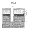
- the multilayer composite film is a three-layer composite film successively comprising, from the initial surface of the substrate, a first layer of silicon, a second layer of alloy Si 1-x Ge x and a third outer layer of silicon.
- the thickness of the layer of alloy Si 1-x Ge x must be sufficient to allow suitable implantation of the indium and is generally of the order of 60 nm.
- the silicon layer, on the Si 1-x Ge x alloy layer must have a thickness at least equal to 5 nm.
- the thickness of the first silicon layer is not critical and is generally less than 100 nm.
- the purpose of using the external silicon layer is to make this first process compatible with the steps of the standard process of manufacture of the transistors, in particular the oxidation stages.
- the multilayer film can be produced in a conventional manner by selective or non-selective epitaxy as will be described below.
- trenches filled with insulating material in the transistors As is well known, it is conventional to make trenches filled with insulating material in the transistors.
- the etching of the trenches and their filling with an insulating material, for example SiO 2 can be done either after formation of the multilayer film, or before as will be described more precisely below.
- the germanium dose must be such that a Si 1-x Ge x layer having the desired composition is obtained and the implantation must be such that the Si 1-x Ge x layer is buried at a depth suitable, i.e. at least 5 nm.
- the germanium implantation can be done by any conventional implantation process, making it possible to obtain the desired Si 1-x Ge x layer.
- the conventional implantation of germanium at doses of 10 12 atoms / cm 2 to 10 16 atoms / cm 2 and energies of 20 keV to 300 KeV are suitable for producing the buried layer of Si 1-x Ge x according to the invention.
- trenches can be etched and filled with insulating material before or after formation of the buried layer of Si 1-x Ge x alloy.
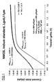
- the first transistor (T1) is a conventional transistor with indium implantation in which indium is implanted in the region of pure silicon channel.
- the implantation of indium has been carried out conventionally under the same conditions at an implantation energy of 170 keV and an implanted dose of 10 13 atoms / cm 2 .
- drain current (I d ) as a function of the gate voltage (V g ) for low and high drain voltages (V d ).
- the transistor T2 has sub-threshold slopes (S) much better than the transistor T1, and which approach the ideal value of 60 mV / decade.
- FIG. 3 which is a graph of the threshold voltage (V th ) as a function of the gate length for the two transistors T1 and T2, shows that the implantation of indium in a layer of SiGe alloy according to the invention , leads to higher electrically active doping, hence better control of the short channel effect.
- one begins by depositing by non-selective epitaxy on the surface of a silicon substrate 1 a tri-layer film 2 comprising a first layer of silicon, a second layer of alloy If 1-x Ge x (10 -5 ⁇ x ⁇ 4.10 -1 ) and a third layer of silicon.
- the percentage of germanium and the thickness of the layer Si 1-x Ge x are chosen so as to respect the condition of non-relaxation of the mechanical stress.
- the two layers of silicon make the process compatible with the steps of a process standard for manufacturing a transistor, in particular the steps oxidation. We then proceed with the implantation of indium as described previously.
- germanium is very reactive towards oxygen, it is preferable, before filling the trench 5 with SiO 2 , to isolate it with a layer of encapsulation material , such as for example silicon oxynitride to prevent any interaction, the SiO 2 filling the trench and the germanium of the three-layer film.
- a layer of encapsulation material such as for example silicon oxynitride to prevent any interaction
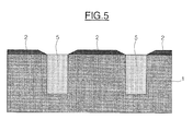
- the three-layer film 2 is then deposited by selective epitaxy according to the invention.
- the three-layer film can be epitaxied on areas active N and P. If one wishes an epitaxy on only the active zones N, it will then be necessary to hide the active zones P.
- Indium is then implanted in the manner described above in the three-layer film and we finish the transistor using the process standard.
- the process begins with the etching of the substrate 1 to form trenches 5 which are then filled with an insulating material (SiO 2 ).
- a film is then deposited by non-selective epitaxy tri-layer 2 continuous, i.e. over the entire surface.
- FIG. 7 schematically illustrates an implementation of the second method of the invention by implanting germanium in a silicon substrate.
- insulating trenches 5 in a silicon substrate 1 After having formed, as described above, insulating trenches 5 in a silicon substrate 1, a resin mask 6 of suitable pattern is formed on the surface and the implantation of germanium is carried out as indicated above to form the layer of alloy Si 1-x Ge x of the invention. The implantation of indium and the completion of the transistor are then carried out in a conventional manner.
- the latter process has the advantage of being simple, rapid and selective and allow a very low concentration of germanium.
Applications Claiming Priority (2)
| Application Number | Priority Date | Filing Date | Title |
|---|---|---|---|
| FR9902513A FR2790598B1 (fr) | 1999-03-01 | 1999-03-01 | NOUVEAU TRANSISTOR A IMPLANTATION D'INDIUM DANS UN ALLIAGE SiGe ET PROCEDES DE FABRICATION |
| FR9902513 | 1999-03-01 |
Publications (1)
| Publication Number | Publication Date |
|---|---|
| EP1033748A1 true EP1033748A1 (fr) | 2000-09-06 |
Family
ID=9542661
Family Applications (1)
| Application Number | Title | Priority Date | Filing Date |
|---|---|---|---|
| EP00400496A Withdrawn EP1033748A1 (fr) | 1999-03-01 | 2000-02-24 | Nouveau transistor à implantation d'indium dans un alliage SiGe et procédés de fabrication |
Country Status (4)
| Country | Link |
|---|---|
| US (1) | US6507091B1 (ja) |
| EP (1) | EP1033748A1 (ja) |
| JP (1) | JP2000307114A (ja) |
| FR (1) | FR2790598B1 (ja) |
Families Citing this family (4)
| Publication number | Priority date | Publication date | Assignee | Title |
|---|---|---|---|---|
| JP3970011B2 (ja) * | 2001-12-11 | 2007-09-05 | シャープ株式会社 | 半導体装置及びその製造方法 |
| JP4136939B2 (ja) * | 2002-01-09 | 2008-08-20 | 松下電器産業株式会社 | 半導体装置およびその製造方法 |
| JP4639040B2 (ja) * | 2002-10-10 | 2011-02-23 | パナソニック株式会社 | 半導体装置の製造方法 |
| US20060068556A1 (en) * | 2004-09-27 | 2006-03-30 | Matsushita Electric Industrial Co., Ltd. | Semiconductor device and method for fabricating the same |
Citations (1)
| Publication number | Priority date | Publication date | Assignee | Title |
|---|---|---|---|---|
| WO1997023000A1 (en) * | 1995-12-15 | 1997-06-26 | Philips Electronics N.V. | SEMICONDUCTOR FIELD EFFECT DEVICE COMPRISING A SiGe LAYER |
Family Cites Families (1)
| Publication number | Priority date | Publication date | Assignee | Title |
|---|---|---|---|---|
| US5272365A (en) * | 1990-03-29 | 1993-12-21 | Kabushiki Kaisha Toshiba | Silicon transistor device with silicon-germanium electron gas hetero structure channel |
-
1999
- 1999-03-01 FR FR9902513A patent/FR2790598B1/fr not_active Expired - Fee Related
-
2000
- 2000-02-24 EP EP00400496A patent/EP1033748A1/fr not_active Withdrawn
- 2000-02-28 JP JP2000051448A patent/JP2000307114A/ja active Pending
- 2000-02-29 US US09/515,787 patent/US6507091B1/en not_active Expired - Fee Related
Patent Citations (1)
| Publication number | Priority date | Publication date | Assignee | Title |
|---|---|---|---|---|
| WO1997023000A1 (en) * | 1995-12-15 | 1997-06-26 | Philips Electronics N.V. | SEMICONDUCTOR FIELD EFFECT DEVICE COMPRISING A SiGe LAYER |
Non-Patent Citations (2)
| Title |
|---|
| BOUILLON P ET AL: "Anomalous short channel effects in Indium implanted nMOSFETs", INTERNATIONAL ELECTRON DEVICES MEETING 1997. IEDM TECHNICAL DIGEST (CAT. NO.97CH36103), INTERNATIONAL ELECTRON DEVICES MEETING. IEDM TECHNICAL DIGEST, WASHINGTON, DC, USA, 7-10 DEC. 1997, 1997, New York, NY, USA, IEEE, USA, pages 231 - 234, XP002118637, ISBN: 0-7803-4100-7 * |
| BOUILLON P ET AL: "RE-EXAMINATION OF INDIUM IMPLANTATION FOR A LOW POWER 0.1MUM TECHNOLOGY", TECHNICAL DIGEST OF THE INTERNATIONAL ELECTRON DEVICES MEETING (IEDM), WASHINGTON, DEC. 10 - 13, 1995, 10 December 1995 (1995-12-10), INSTITUTE OF ELECTRICAL AND ELECTRONICS ENGINEERS, pages 897 - 900, XP000624815, ISBN: 0-7803-2701-2 * |
Also Published As
| Publication number | Publication date |
|---|---|
| FR2790598A1 (fr) | 2000-09-08 |
| US6507091B1 (en) | 2003-01-14 |
| FR2790598B1 (fr) | 2001-06-01 |
| JP2000307114A (ja) | 2000-11-02 |
Similar Documents
| Publication | Publication Date | Title |
|---|---|---|
| EP1837916B1 (fr) | Procédé de réalisation d'un transistor à canal comprenant du germanium | |
| EP0164281B1 (fr) | Procédé de fabrication d'une couche isolante enterrée dans un substrat semiconducteur, par implantation ionique | |
| FR2616590A1 (fr) | Procede de fabrication d'une couche d'isolant enterree dans un substrat semi-conducteur par implantation ionique et structure semi-conductrice comportant cette couche | |
| FR2821483A1 (fr) | Procede de fabrication d'un transistor a grille isolee et a architecture du type substrat sur isolant, et transistor correspondant | |
| EP0426251A1 (fr) | Procédé pour fabriquer un dispositif à transistors MIS ayant une électrode de grille en forme de "T" inversé | |
| FR2652448A1 (fr) | Procede de fabrication d'un circuit integre mis haute tension. | |
| FR2823009A1 (fr) | Procede de fabrication d'un transistor vertical a grille isolee a faible recouvrement de la grille sur la source et sur le drain, et circuit integre comportant un tel transistor | |
| FR2795554A1 (fr) | Procede de gravure laterale par trous pour fabriquer des dis positifs semi-conducteurs | |
| FR2468208A1 (fr) | Dispositif semiconducteur avec une diode zener | |
| EP0577498B1 (fr) | Transistor JFET vertical à mode de fonctionnement bipolaire optimisé et procédé de fabrication correspondant | |
| EP0797252B1 (fr) | Substrat de type silicium sur isolant pour la fabrication de transistors et procédé de préparation d'un tel substrat | |
| FR2806833A1 (fr) | Procede de fabrication d'un transistor mos a deux grilles, dont l'une est enterree, et transistor correspondant | |
| FR3067516A1 (fr) | Realisation de regions semiconductrices dans une puce electronique | |
| EP1218942A1 (fr) | Dispositif semi-conducteur combinant les avantages des architectures massives et soi, et procede de fabrication | |
| EP1033748A1 (fr) | Nouveau transistor à implantation d'indium dans un alliage SiGe et procédés de fabrication | |
| FR2818012A1 (fr) | Dispositif semi-conducteur integre de memoire | |
| FR2795868A1 (fr) | Transistor mosfet a effet canal court compense par le materiau de grille | |
| EP1146561A1 (fr) | Procédé de réalisation d'un transistor bipolaire | |
| FR2791178A1 (fr) | NOUVEAU DISPOSITIF SEMI-CONDUCTEUR COMBINANT LES AVANTAGES DES ARCHITECTURES MASSIVE ET soi, ET PROCEDE DE FABRICATION | |
| EP4088312B1 (fr) | Procédé de fabrication d'une structure de type semi-conducteur sur isolant pour applications radiofréquences | |
| EP1328969B1 (fr) | Procédé de formation d'un transistor mos | |
| EP2551899A1 (fr) | Procédé ameliore de réalisation de tranchées d'isolation dans un substrat semi-conducteur sur isolant | |
| EP4235765A2 (fr) | Procédé amélioré de fabrication d'un circuit intégré comportant un transistor nmos et un transistor pmos | |
| FR2762138A1 (fr) | Transistor mos a fort gradient de dopage sous sa grille | |
| EP0607075B1 (fr) | Composant électronique semi-conducteur à résistance dynamique négative, méthodes d'utilisation et procédé de fabrication correspondants |
Legal Events
| Date | Code | Title | Description |
|---|---|---|---|
| PUAI | Public reference made under article 153(3) epc to a published international application that has entered the european phase |
Free format text: ORIGINAL CODE: 0009012 |
|
| AK | Designated contracting states |
Kind code of ref document: A1 Designated state(s): DE FR GB IT |
|
| AX | Request for extension of the european patent |
Free format text: AL;LT;LV;MK;RO;SI |
|
| 17P | Request for examination filed |
Effective date: 20000911 |
|
| AKX | Designation fees paid |
Free format text: DE FR GB IT |
|
| RAP1 | Party data changed (applicant data changed or rights of an application transferred) |
Owner name: STMICROELECTRONICS S.A. Owner name: FRANCE TELECOM |
|
| 17Q | First examination report despatched |
Effective date: 20070710 |
|
| STAA | Information on the status of an ep patent application or granted ep patent |
Free format text: STATUS: THE APPLICATION IS DEEMED TO BE WITHDRAWN |
|
| 18D | Application deemed to be withdrawn |
Effective date: 20071121 |