EP1020057B1 - Fsk demodulator using a superlinear integrator - Google Patents
Fsk demodulator using a superlinear integrator Download PDFInfo
- Publication number
- EP1020057B1 EP1020057B1 EP98953198A EP98953198A EP1020057B1 EP 1020057 B1 EP1020057 B1 EP 1020057B1 EP 98953198 A EP98953198 A EP 98953198A EP 98953198 A EP98953198 A EP 98953198A EP 1020057 B1 EP1020057 B1 EP 1020057B1
- Authority
- EP
- European Patent Office
- Prior art keywords
- signal
- circuitry
- value
- integration
- bit
- Prior art date
- Legal status (The legal status is an assumption and is not a legal conclusion. Google has not performed a legal analysis and makes no representation as to the accuracy of the status listed.)
- Expired - Lifetime
Links
Images

Classifications
-
- H—ELECTRICITY
- H04—ELECTRIC COMMUNICATION TECHNIQUE
- H04L—TRANSMISSION OF DIGITAL INFORMATION, e.g. TELEGRAPHIC COMMUNICATION
- H04L27/00—Modulated-carrier systems
- H04L27/10—Frequency-modulated carrier systems, i.e. using frequency-shift keying
- H04L27/14—Demodulator circuits; Receiver circuits
- H04L27/156—Demodulator circuits; Receiver circuits with demodulation using temporal properties of the received signal, e.g. detecting pulse width
- H04L27/1563—Demodulator circuits; Receiver circuits with demodulation using temporal properties of the received signal, e.g. detecting pulse width using transition or level detection
Definitions
- the present invention relates generally to the field of process control instruments. More particularly, the present invention relates to systems and methods for facilitating serial communication within a process control instrument.
- Transmitters in the process control industry typically communicate with a controller over a two-wire circuit or control loop.
- the transmitter receives commands from a controller over the two-wire control loop and sends output signals representative of a sensed physical parameter back to the controller.
- the transmitter itself can include a number of devices such as microprocessors, memory devices, analog-to-digital convertors, digital-to-analog convertors, digital signal processors (DSPs), sensors, and other peripheral devices.
- Communication between the various devices inside of the transmitter typically takes place on a data bus which includes a clock line and a number of data lines. Because of concerns about current consumption and complexity, it is important to minimize the number of data bus lines required for communication between the various devices.
- the sensor of the process control instrument must be electrically isolated from measurement circuitry or other devices in the process control instrument for safety purposes.
- An isolation barrier is used to electrically isolate the sensor from the rest of the circuitry within the transmitter. The sensor receives power and communicates with the measurement circuitry through the barrier. The barrier prevents harmful electrical discharges, sometimes present on the process control loop, from entering the measurement circuitry. While necessary for safety or other purposes, inclusion of the isolation barrier reduces the number of electrical connections allowed between the sensor and the other devices for communication, clock information and power. Conventional serial communications techniques used to transmit data across the isolation barrier frequently result in undesirably high levels of power consumption and/or complex circuitry.
- U.S. Patent No. 4,021,744 (document D1) to Nicola Montefusco is directed toward a demodulator for frequency-keyed communication systems.
- demodulators are disclosed which distinguish between two closely adjoining input frequencies. See D1 at col. 1, lines 58-61.
- the disclosed demodulator is for a communication system of the type wherein two keying frequencies are alternately generated to transmit information, e.g. as dots and dashes of the Morse code or as marks and spaces of the Baudot code. See D1 at col. 1, lines 6-10.
- the demodulators disclosed in the Montefusco patent includes an amplitude limiter LM which receives an incoming oscillation which alternates between two keying frequencies, and which provides in response a square wave.
- a zero-crossing detector DF delivers a train of signal pulses c to the reset input of a pulse counter CN whose stepping input receives a succession of clock pulses.
- the output of the pulse counter is fed into a digital comparator CM and is compared to a fixed numerical value which should be not less than the count K obtained from one keying frequency, but should be well below the count K + X obtained from the second keying frequency.
- the comparator CM emits a sequence of rectangular pulses coinciding with respective half-cycles of the oscillations incoming to the demodulator. These pulses are integrated in a low-pass filter LP whose output voltage, upon surpassing a threshold level, provides a rectangular pulse indicative of the keying frequency. See D1 at col. 2, lines 22-60.
- a method of and apparatus for decoding an encoded signal are disclosed.
- a first bit of the encoded signal is received and integrated with a super linear integrator to provide a first integration signal.
- a first reference signal is provided as a function of a previous integration signal associated with a previous bit of the encoded signal by multiplying the previous integration signal by an amount greater than one if the previous bit has a first value, and by multiplying the previous integration signal by an amount less than one if the previous bit has a second value.
- the first integration signal is compared to the first reference signal and a first bit of an output signal is provided based upon the comparison.
- the first bit of the output signal is indicative of information encoded in the first bit of the encoded signal.
- the method and apparatus of the present invention are particularly adapted for communicating serially across a barrier in a process control instrument.
- a housing for the process control instrument has a first compartment, a second compartment, and an electrical barrier between the first and second compartments.
- Encoding circuitry in the first compartment is coupled to the barrier for encoding data in a signal for transmission across the barrier. Cycles of the signal having a first period are representative of a first data state, while cycles of the signal having a second period are representative of a second data state.
- Decoding circuitry in the second compartment is coupled to the barrier and receives and decodes the signal having the varying period.
- the encoded signal has a fifty percent duty cycle to reduce power consumption by the barrier and to improve the quality of the transmitted signal.
- the decoding circuitry of the present invention can be used to decode either frequency modulated signals or pulse width modulated signals.
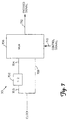
- FIG. 1 is a simplified block diagram of a transmitter 10 which uses the serial communications techniques of the present invention for communicating between various devices within or associated with the transmitter.
- transmitter 10 includes housing 11, measurement circuitry 16 and sensor circuitry 18.
- Measurement circuitry 16 is positioned in compartment 17 of housing 11.
- Sensor circuitry 18 is positioned in compartment 19 of housing 11. Portions of sensor circuitry 18 can also be located externally from housing 11 as well.
- Measurement circuitry 16 couples to two-wire loop 12 via connection terminals 14 and is used for sending and receiving information on loop 12.
- Loop 12 couples to a control room which is modeled as power source 15 and resistor 13.
- Measurement circuitry 16 and/or sensor circuitry 18 can include multiple nodes of two types: master nodes which are typically microprocessors or slave nodes which are typically peripheral devices such as memory.
- Other examples of peripheral devices which can be included within measurement circuitry 16 or sensor circuitry 18 are devices for extracting power for the transmitter from current flowing through loop 12, modems and other communications and I/O devices, signal processing devices, display devices, analog-to-digital convertors, digital-to-analog convertors, temperature sensors, flow sensors, pH sensors, level sensors, pressure sensors, differential pressure sensors, etc.
- measurement circuitry 16 and sensor circuitry 18 are located in separate compartments 17 and 19 within transmitter 10 and are electrically isolated by isolators 20 and 25.
- the isolators can be transformers, optical barriers, or other isolation barriers known in the art and required for electrically isolating sensor circuitry 18 and the process from measurement circuitry 16.
- the isolators can also reduce ground loop noise in the measurement of the parameters sensed by sensor circuitry 18.
- Transmission lines 22 and 24 couple measurement circuitry 16 and sensor circuitry 18 to isolator 20 for facilitating communication between sensor circuitry 18 and measurement circuitry 16 across isolator 20.
- lines 22 and 24 represent a single data line across which information must be transmitted serially from measurement circuitry 16, through isolator 20, to sensor circuitry 18. Likewise, information is transmitted serially from sensor circuitry 18, through isolator 25, to measurement circuitry 16.
- measurement circuitry 16 includes frequency modulator or encoder circuit 30, decoder circuit 31, microprocessor 32, digital signal processing circuit 33 and input/output (I/O) circuitry 34.
- I/O circuitry 34 is coupled to microprocessor 32 and to loop 12 for receiving data and instructions over loop 12, for transmitting data over the loop, and for regulating power from the loop to transmitter 10.
- Microprocessor 32 is coupled to I/O circuitry 34, to modulator 30 and to decoder 31 via DSP circuit 33 for receiving, transmitting and processing signals and data from/to the various devices of transmitter 10.
- microprocessor 32 is used to control the operation of transmitter 10.
- Modulator 30 frequency modulates signals to be transmitted across transmission line 24, isolator 20 and transmission line 22 to sensor circuitry 18.
- Decoder 31 receives modulated signals transmitted across transmission line 27, isolator 25 and transmission line 29 from sensor circuitry 18.
- Sensor circuitry 18 includes control registers 21, modulator or encoder circuit 23, sensor 26, signal conversion circuitry 28, and decoder 100.
- Sensor 26 senses a process variable and provides an output to signal conversion 28.
- Circuitry 28 can include sigma-delta modulators, complete A/D converters, or other signal conversion circuitry.
- Modulator 23 can be of the type like modulator 30 which frequency modulates process variable related signals to be transmitted across transmission line 27, isolator 25 and transmission line 29 to measurement circuitry 16. However, other modulation techniques can be used to transmit signals across isolator 25.
- Decoder 100 decodes the frequency modulated signal transmitted across the isolation barrier from modulator 30 according to the present invention.
- the signal transmitted across isolator 20 carries encoded information and is used to create a clock signal for use in the operation of sensor circuitry 18.
- the decoded signal is provided to other circuitry within sensor circuitry 18, for example control registers 21, and can be used to control the various devices within sensor circuitry 18.
- Control registers 21 control test functions, filter functions, and the like. While in other embodiments, measurement circuitry 16 and sensor circuitry 18 can include devices other than those illustrated in FIG. 1, in some embodiments, modulators 23 and 30 and decoders 31 and 100 are used to transmit or pass information between measurement circuitry 16 and sensor circuitry 18.
- Transmitter 10 is connected to a controller, electrically modeled as voltage source 15 and resistor 13, which can provide all the power to transmitter 10.
- sensor circuitry 18 also includes rectifier circuitry for rectifying the signal transmitted across isolator 20 to provide power for sensor circuitry 18.
- sensor circuitry 18 and measurement circuitry 17 can alternatively be line powered from an external power supply, as in a magmeter.
- the current in the process control loop (formed by transmitter 10, source 15 and resistor 13) is typically representative of a process variable sensed by sensor 26 in transmitter 10, or of a control signal from transmitter 10.
- the current ranges between 4 and 20 mA, according to the ISA 4-20 mA standard. Accordingly, transmitter 10 must operate on less than 4 mA.
- Transmitter 10 can also be configured to communicate digitally over the 4-20 mA current, as in the HART® protocol, or can be fully digital communications as in Fieldbus.
- the present invention includes a method and apparatus for providing serial communication across isolation circuits such as isolators 20 and 25 shown in FIG. 1. For ease of illustration, only encoding and decoding of signals transmitted across isolator 20 is discussed. However, the same techniques and features can be used to encode and decode signals transmitted across isolator 25 as well.
- a serial data stream is encoded by modulator 30 using a frequency or period modulation technique. A logical "0" (first data state) is transmitted as a cycle of the signal having a first period To and a logical "1" (second data state) is transmitted as a cycle of the signal having a second period T 1 different than the first period.
- a serial data stream encoded in this manner is illustrated in FIG. 2.
- T 1 is set to approximately 1.10 ⁇ s (F 1 ⁇ 900 KHz)
- T 0 is set to approximately 0.55 ⁇ s (F 0 ⁇ 1.8 MHz).
- F 1 is set to approximately 460.5 KHz
- F 0 is set to approximately 921 KHz.
- An encoded data stream such as illustrated in FIG. 2 is transmitted across isolation barrier 20 in accordance with the present invention, and subsequently decoded by decoder circuit 100.
- Pulse width modulation can result in saturation of the transformer core in transformer type isolation barriers. If the transformer core saturates, power is lost in the core causing the transformer to heat. The generation of unnecessary heat around electronic instruments is undesirable as it contributes to component failures, reduced component life expectancies and degradations in the electrical performance of the components. Also, wasted power is highly undesirable, particularly in process control instruments where power is supplied over the loop. Further, the saturated core of the transformer distorts the signal, leading to transmission errors.
- the encoded signals are approximately fifty percent duty cycle signals regardless of the period of each individual cycle of the signal.
- the encoded signals of the present invention are potentially easier to generate than in pulse width modulation techniques.
- the fifty percent duty cycle signals should provide more constant power consumption as compared to pulse width modulation encoded signals.
- the symmetry of a fifty percent duty cycle signal should help to reduce the harmonics associated with the signal, reducing interference on nearby components.
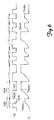
- FIG. 2 illustrates eight consecutive cycles 50, 52, 54, 56, 58, 60, 62 and 64 of an encoded signal. Each cycle represents one bit of transmitted data. Alternatively, each cycle can represent one of multiple possible data states for transmission between devices. During each cycle, rising edge (transition) 68 and trailing edge (transition) 70 are preferably timed such that the signal has approximately a fifty percent duty cycle, regardless of the period of the signal during the cycle. As shown, cycles 50, 52, 54, 60 and 64 have periods T 0 (at frequency F 0 ). Cycles 56, 58 and 62 of the signal have periods T 1 (at frequency F 1 ). Therefore, in a two data state implementation of the present invention, the data stream of FIG. 2 would represent the sequence 00011010.
- FIG. 3 One circuit for decoding the period encoded data of FIG. 2 is shown in FIG. 3, although other implementations are possible.
- a circuit for encoding the period encoded data of FIG. 2 is shown in FIG. 7.
- serial data decoding circuit 100 illustrated in FIG. 3 a single data stream encoded using the technique of FIG. 2 and transmitted across an isolation transformer or other barrier can be decoded.
- decoding circuit 100 can be used to decode pulse width modulated data streams as well.
- the circuit illustrated in FIG. 3 is well suited for use in measurement circuitry 16 and/or sensor circuitry 18 to decode data transmitted across an isolation barrier.
- the methods and circuits of the present invention can be used to facilitate improved serial data communications on any appropriate data buses or other data lines.
- Decoder circuit 100 includes current generator 102, reference current generator 104, edge triggered comparator 106 and output circuitry 108.
- Current generator 102 includes switch S 1 , capacitor C 1 , current sink I C , transconductance amplifier stage 110 and track and hold circuit 118.
- Input 112 of transconductance amplifier 110 is coupled to supply voltage V DD .
- Capacitor C 1 and switch S 1 are coupled in parallel across inputs 112 and 114 of amplifier 110.
- Current sink I C is coupled between input 114 of amplifier 110 and supply voltage V SS .
- Output 116 of amplifier 110 provides current I gm as an input to track and hold circuit 118.
- Track and hold circuit 118 provides at outputs 120 and 122 currents I S (t) which are delayed versions of I gm .
- Switch S 1 is controlled using the incoming encoded data signal CK. During the high voltage portions of the CK signal duty cycle, switch S 1 opens. Switch S 1 , capacitor C 1 , current sink I C and transconductance amplifier 110 together form super linear integration circuit.
- output current I gm at output 116 of amplifier 110 will have one of two period or frequency dependent final values, with each final value corresponding to one of the two data states encoded.
- the circuit can be adapted to provide three or more output states corresponding to three or more possible data states.
- Track and hold circuit 118 maintains current I gm during the low voltage portions of the CK signal duty cycle such that output current I s (t) of track and hold circuit 118 is maintained substantially the same as I gm during the low voltage portion of the CK signal.
- Track and hold circuit 118 is implemented using a switched current mirror of the type which maintains the output current even after the input current has changed. Alternatively, a voltage type sample and hold (S/H) circuit can be used.
- Output current I s (t) from circuit 118 is provided to comparator 106 at input 120, and to reference current generator 104 at input 122. Thus, current I s (t) is mirrored such that it can be provided at two track and hold circuit outputs. Operation of current generator 102 is discussed and shown in further detail with reference to FIG.s 5 and 6. However, for ease of illustration, only generation of one I s (t) output current is shown in FIG.s 5 and 6.
- Reference current generator 104 generates a reference current I REF which is provided to edge triggered comparator 106 for comparison to current I s (t). With current I c appropriately adjusted, reference current generator 104 generates a substantially constant reference current for any given set of encoded input signal frequencies, and automatically adjusts the reference current appropriately if I s (t) varies slightly due to process or temperature.
- Reference current generator 104 includes current delay cell 124, switch S 2 , multiplier circuit 128 and multiplier circuit 129.
- Current delay cell 124 can be a switched current mirror or other well known circuits which receive as an input current I s (t), which maintain that input current for a period of time ⁇ , and then provide at a later time substantially the same current as I S (t- ⁇ ).
- current delay cell 124 provides at its output 126 a current approximately equal to current I S (t) from the previous cycle of the incoming encoded data signal CK.
- ⁇ will have one of two values depending upon the sequence of data states received by decoder 100. When the previous and current bits each represent logical "0" data states, ⁇ will be approximately equal to T 0 . When the previous and current bits each represent logical "1" data states, ⁇ will be approximately equal to T 1 . When the previous and current bits represent a transition from a logical "1" data state to a logical "0" data state, or vice versa, ⁇ will be approximately equal to 1/2*(T 0 + T 1 ).
- switch S 2 couples output 126 of current delay cell 124 to one of multiplier circuits 128 and 129. If selected, multiplier circuit 128 multiplies current I S (t- ⁇ ) by 0.75, while multiplier circuit 129 multiplies current I S (t- ⁇ ) by 1.5.
- Other multiplication factors can be used if frequencies other than 900 MHz and 1.8 MHz are used to encode the data in the high accuracy mode of operation, for example. Large variations in I s (t), as would occur when switching between the high accuracy and low power frequency ranges, are prevented or accommodated by controlling current I C in order to change the integration rate of the super linear integrator. Generally, I C is controlled so that current I s (t) is nominally always at about the same value.
- comparator 106 Because comparator 106 is edge triggered, output Q(t) will correspond to the previous encoded bit until the comparator again latches. Therefore, with current delay cell 124 also providing current I s (t- ⁇ ) corresponding to the previous decoded bit, switch 52 is controlled such that the correct multiplication circuit is chosen to provide reference current I REF .
- current I C can be controlled so that current generator 104 provides an appropriate reference current regardless of the particular set of periods (and therefore regardless of the possible values of I SMIN and I SMAX ) chosen to represent the logic levels in the data stream.
- the reference current I REF is maintained during slight variations in I s (t), caused by temperature or process variations, by the appropriate selection of multipliers 128 and 129.
- decoder circuit 100 can be used to decode signals encoded with any of a wide range of sets of periods.
- This adaptability, along with I C modification, allows the periods to be selected or changed as may be convenient or necessary without modifying circuit 100.
- the ability to tailor the signal periods without modifying the circuitry saves time and costs.
- the use of multiplication circuits 128 and 129 allows an adequate reference current to be generated when small variations in the incoming data or clock signal CK occur.
- Current comparator 106 receives current I S (t) from output 120 of current generator 102 at one of its inputs. Current comparator 106 receives at its other input reference current I REF from output 130 of reference current generator 104. At output 132, comparator 106 provides a high or low voltage output, depending upon whether current I S (t) is greater or lesser than reference current I REF . Thus, comparator output 132 is indicative of whether a particular bit of the encoded signal received at switch S 1 contained an encoded "1" or a "0".
- comparator 106 is preferably a current comparator
- all or parts of decoder circuit 100 can be implemented using voltage mode circuits instead of current mode circuits.
- current generator 102 can be replaced by a voltage generating circuit.
- reference current generator 104 could be replaced with a reference voltage generator circuit.
- comparator 106 would-be replaced with a voltage comparator circuit.
- current-mode circuits such as those illustrated in FIG. 3 are preferred.
- Output circuit 108 includes current source I V , capacitor C V , AND gate 136, and latch circuitry 140.
- Current source I V is coupled between supply voltage V DD and input 134 to AND gate 136.
- Input 134 to AND gate 136 is also coupled through capacitor C V to supply voltage V SS .
- Output 132 of comparator 106 is coupled to input 135 to AND gate 136.
- Output signal Q(t) of AND gate 136 is provided at input 138 to latch circuitry 140.
- Latch circuitry 140 provides an output at 142 which is representative of the state of the data stream encoded in signal CK.
- Current source I V and capacitor C V cooperate to maintain input 134 of AND gate 136 at a low logic level voltage immediately after a reset or at start-up.
- output Q(t) is held low for several cycles after start-up until capacitor C V sufficiently charges. This prevents false outputs due to noise or other power-up process conditions.
- a power on reset circuit can be used to drive input node 134 of AND gate 136.
- Latch circuitry 140 receives AND gate output Q(t) as an input and provides an output at output 142. Latch 140 is used to latch the individual decoded bits, corresponding to the encoded bits received in the serial data stream CK, to other circuitry in the transmitter.
- FIG. 4 is a timing diagram which illustrates output Q(t) as a function of input signal CK.
- FIG. 4 illustrates the decoded bit (in signal Q(t)) for each bit or cycle of the period encoded data signal CK.
- Output Q(t) changes to its corresponding value for each bit of encoded signal CK at midpoint (or falling edge 402) of the corresponding received period encoded bit.
- Q(t) transitions (at rising edge 404) from a "0" to "1" at midpoint (i.e. falling edge 402) of the received period encoded "l” bit.
- Q(t) transitions at the falling edges of the corresponding bit of the received period encoded signal
- numerous other implementations are possible.
- Q(t) can be designed to transition at the start (rising edge 406) of the next encoded bit received.
- FIG. 5 is a circuit diagram which illustrates current generator 102 in greater detail.
- current generator 102 is divided functionally into super-linear integration circuit 502 and track and hold circuit 118.
- Integration circuit 502 includes switch S 1 , capacitor C 1 , current source I C and transconductance amplifier 110.
- transconductance amplifier 110 includes transistors Q MN1 and Q MN2 and current source I D , configured as a differential amplifier.
- Transconductance amplifier 110 cooperates with switch S 1 , capacitor C 1 and current source I C to form a super-linear integration circuit which provides an output current I gm having a magnitude which is dependent upon the period length of the cycle of the encoded input signal CK.
- Track and hold circuit 118 includes transistors Q MP1 and Q MP2 , capacitor C 2 , and reset switch S 3 .
- Transistors Q MP1 , transistor Q MP2 , capacitor C 2 and switch S 3 are configured as a switched current mirror.
- Current generator 102 functions generally as follows. During the high voltage portion of each encoded cycle or bit of signal CK, switch S 1 is opened. During this time, capacitor C 1 charges and voltage V 1 drops. Thus, with the control node of transistor Q MN2 coupled to voltage source V DD , a voltage differential develops between the control nodes of transistors Q MN1 and Q MN2 , causing a greater portion of current I D to pass through transistor Q MN2 . Since turn-on current I 1 is very small as compared to current I D , the current flowing through transistor Q MN2 will be close in magnitude to that of current I gm which flows into transistor Q MP1 of track and hold circuit 118.
- switch S 3 is closed when switch S 1 is open and vice versa. As illustrated, both switches S 1 and S 3 are PMOS type switches. However, other switch types can be used with slight modifications.
- switch S 3 closes, and track and hold circuit 118 operates as a current mirror. Thus current I S flowing through transistor Q MP2 will be approximately equal to current I gm .
- switch S 3 opens and the charge on capacitor C 2 keeps transistor Q MP2 conducting so that output current I S is maintained, even as current I gm changes.
- this switched current mirror design maintains the current generated by transconductance stage 110 for use during the next half cycle. Switched current mirrors of the type used for track and hold device 118 can also be used as current delay cell 124.
- FIG. 6 illustrates the correspondence between current I s from current generator 102 and the incoming encoded signal CK.
- current I S takes on its minimum active current value I SMIN .
- I S drops to substantially zero.
- current I S takes on its maximum value I SMAX . This continues for each bit or cycle of incoming data signal CK, with current I S taking on either value I SMIN or value I SMAX .
- Track and hold circuit 118 maintains the current value (either at I SMIN or at I SMAX ) for the remainder of the cycle of the encoded bit.
- switch S 3 causes current I S to reset to 0.
- FIG. 7 illustrates one preferred embodiment of modulator 30 used in accordance with the present invention to frequency or period encode signals for transmission across isolator 20.
- Modulator 30 includes a clock signal CLOCK having approximately a 50 percent duty cycle, frequency divider 702 and multiplexer 706.
- the 50 percent duty cycle clock signal CLOCK can have, for example, the frequency F 0 corresponding to transmission of a logical 0 bit.
- This clock signal is provided both to input 703 of frequency divider 702 and input 708 of multiplexer 706.
- a signal having a 50 percent duty cycle but approximately one-half the frequency of clock signal CLOCK is provided to multiplexer 706 at input 704.
- output 712 of multiplexer 706 is selectively connected to the appropriate one of inputs 704 and 708 during each individual cycle. In this manner, a frequency encoded signal having a duty cycle of approximately 50 percent can be generated at output 712.
- the present invention provides numerous advantages over the prior art. For example, the use of a super linear integration circuit helps to increase the integrated signal difference between encoded bits of the first and second data states. This in turn provides greater noise immunity and reduces the likelihood that transmission errors will occur. Also, preferred embodiments of the present invention require only a single integration circuit.
- the single integration channel nature of the decoder of the present invention reduces complexity and costs as compared to prior art two integration channel decoders.
- use of a fifty percent duty cycle signal to encode the transmitted data reduces heat generation, reduces data losses and errors caused by distorted signals from saturated barrier transformers, and decreases interference with nearby components which can sometimes result from harmonics in non-fifty percent duty cycle signals. Additionally, fifty percent duty cycle signals decrease the decoder circuit complexity and increase the ease at which the encoded signal is generated.
- the methods and circuits of the present invention can be implemented using various hardware, software and hardware/software combinations to encode and decode the data signals in order to transmit and receive messages.
- the present invention is particularly well adapted for use in process control transmitters, valve controllers, and in process control field devices in general because of the low current consumption of the present invention.
- the term process control instrument is intended to mean any of these and other process control devices.
- the present invention can be utilized in any of a wide variety of applications in which devices on a printed circuit board or coupled to a data line in general are required to communicate with each other.
- the present invention is described primarily with respect to encoding and decoding logical ones and zeros, the present invention can also be used to implement multi-state communications in which more than two data states are encoded.
- the single super linear integration circuit and other decoding circuitry can be used to decode either pulse width modulated or frequency modulated signals with little or no modification.
- Terms such as decoding circuitry, integration circuitry and current generator circuitry can all be used to refer to transition detecting circuitry of the type which detects transitions in an encoded signal for purposes of decoding the signal.
Landscapes
- Engineering & Computer Science (AREA)
- Computer Networks & Wireless Communication (AREA)
- Signal Processing (AREA)
- Analogue/Digital Conversion (AREA)
- Digital Transmission Methods That Use Modulated Carrier Waves (AREA)
- Compression, Expansion, Code Conversion, And Decoders (AREA)
- Arrangements For Transmission Of Measured Signals (AREA)
- Synchronisation In Digital Transmission Systems (AREA)
Applications Claiming Priority (3)
| Application Number | Priority Date | Filing Date | Title |
|---|---|---|---|
| US08/941,949 US6021162A (en) | 1997-10-01 | 1997-10-01 | Vortex serial communications |
| US941949 | 1997-10-01 | ||
| PCT/US1998/020274 WO1999017508A1 (en) | 1997-10-01 | 1998-09-28 | Fsk demodulator using a super linear integrator |
Publications (2)
| Publication Number | Publication Date |
|---|---|
| EP1020057A1 EP1020057A1 (en) | 2000-07-19 |
| EP1020057B1 true EP1020057B1 (en) | 2004-02-18 |
Family
ID=25477339
Family Applications (1)
| Application Number | Title | Priority Date | Filing Date |
|---|---|---|---|
| EP98953198A Expired - Lifetime EP1020057B1 (en) | 1997-10-01 | 1998-09-28 | Fsk demodulator using a superlinear integrator |
Country Status (9)
| Country | Link |
|---|---|
| US (1) | US6021162A (enExample) |
| EP (1) | EP1020057B1 (enExample) |
| JP (1) | JP4021144B2 (enExample) |
| CN (1) | CN1106101C (enExample) |
| AT (1) | ATE260009T1 (enExample) |
| BR (1) | BR9812614A (enExample) |
| CA (1) | CA2305425A1 (enExample) |
| DE (1) | DE69821784T2 (enExample) |
| WO (1) | WO1999017508A1 (enExample) |
Cited By (1)
| Publication number | Priority date | Publication date | Assignee | Title |
|---|---|---|---|---|
| EP3486738B1 (en) * | 2013-08-06 | 2022-03-23 | Bedrock Automation Platforms Inc. | Programmable discrete input module and respective method |
Families Citing this family (15)
| Publication number | Priority date | Publication date | Assignee | Title |
|---|---|---|---|---|
| FR2774232B1 (fr) * | 1998-01-26 | 2000-02-25 | Alsthom Cge Alcatel | Dispositif de generation d'impulsions de courant a faible bruit, comparateur de phase, synthetiseur et utilisation correspondants |
| WO2002041086A2 (en) | 2000-11-16 | 2002-05-23 | Invensys Systems, Inc. | Control system methods and apparatus for inductive communication across an isolation barrier |
| KR100536188B1 (ko) * | 2001-11-14 | 2005-12-14 | 한국과학기술연구원 | 인체 등의 매질을 통신선로로 이용한 매질 내외간의 통신방법 및 장치 |
| US6885949B2 (en) * | 2002-07-24 | 2005-04-26 | Smar Research Corporation | System and method for measuring system parameters and process variables using multiple sensors which are isolated by an intrinsically safe barrier |
| DE102005041455A1 (de) * | 2005-08-31 | 2007-03-15 | Abb Patent Gmbh | Automatisierungstechnische Einrichtung |
| WO2008154504A2 (en) * | 2007-06-08 | 2008-12-18 | William Marsh Rice University | System and method for intra-body communication |
| JP5023836B2 (ja) * | 2007-06-25 | 2012-09-12 | 横河電機株式会社 | 2線式フィールド機器 |
| US9217653B2 (en) * | 2007-09-13 | 2015-12-22 | Rosemount Inc. | High performance architecture for process transmitters |
| TWI583187B (zh) * | 2013-07-30 | 2017-05-11 | 聯詠科技股份有限公司 | 資料處理方法及裝置 |
| CN104347101B (zh) * | 2013-08-08 | 2017-10-27 | 联咏科技股份有限公司 | 数据处理方法及装置 |
| US10663331B2 (en) | 2013-09-26 | 2020-05-26 | Rosemount Inc. | Magnetic flowmeter with power limit and over-current detection |
| JP6964968B2 (ja) * | 2016-09-28 | 2021-11-10 | 新コスモス電機株式会社 | 電気機器および電気機器の信号に重畳するノイズを低減する方法 |
| US10277216B1 (en) * | 2017-09-27 | 2019-04-30 | Apple Inc. | Wide range input voltage differential receiver |
| CN109635908B (zh) * | 2018-12-13 | 2020-09-11 | 中山大学 | 数模混合解码电路、解码方法及系统架构 |
| CN112542996A (zh) * | 2019-09-20 | 2021-03-23 | 中国科学院微电子研究所 | 陀螺数字信号的高阶同步积分解调电路和方法 |
Family Cites Families (38)
| Publication number | Priority date | Publication date | Assignee | Title |
|---|---|---|---|---|
| US3905029A (en) * | 1970-12-01 | 1975-09-09 | Gen Motors Corp | Method and apparatus for encoding and decoding digital data |
| US3760412A (en) * | 1971-07-01 | 1973-09-18 | R Barnes | Rate adaptive nonsynchronous demodulator apparatus |
| US4053834A (en) * | 1973-04-12 | 1977-10-11 | Textron, Inc. | Narrowband phase modulation communication system which eliminates thresholding |
| US3852809A (en) * | 1973-07-05 | 1974-12-03 | Ibm | Return to zero detection circuit for variable data rate scanning |
| US3909629A (en) * | 1974-01-23 | 1975-09-30 | Ibm | H-Configured integration circuits with particular squelch circuit |
| IT1037127B (it) * | 1975-03-18 | 1979-11-10 | Sits Soc It Telecom Siemens | Demodulatore di onde modulate in frequenza |
| US4032915A (en) * | 1975-07-23 | 1977-06-28 | Standard Oil Company (Indiana) | Speed-tolerant digital decoding system |
| US4007331A (en) * | 1975-08-13 | 1977-02-08 | Bunker Ramo Corporation | Apparatus for demodulation of relative phase modulated binary data |
| NL7700318A (nl) * | 1976-01-16 | 1977-07-19 | Little Inc A | Werkwijze en inrichting voor communicatie over elektrische krachtleidingen. |
| US4100531A (en) * | 1977-02-03 | 1978-07-11 | Nasa | Bit error rate measurement above and below bit rate tracking threshold |
| US4312070A (en) * | 1979-12-07 | 1982-01-19 | Motorola, Inc. | Digital encoder-decoder |
| US4501000A (en) * | 1981-07-27 | 1985-02-19 | Sony Corporation | Method of coding binary data |
| DE3131845A1 (de) * | 1981-08-12 | 1983-02-24 | Brown, Boveri & Cie Ag, 6800 Mannheim | Verfahren zum erzeugen und erfassen digitaler signale beliebiger zeichencodierung |
| US4425645A (en) * | 1981-10-15 | 1984-01-10 | Sri International | Digital data transmission with parity bit word lock-on |
| US4485448A (en) * | 1982-02-26 | 1984-11-27 | Sperry Corporation | Apparatus and method for detecting the onset of a frequency shift keyed signal |
| US4592072B1 (en) * | 1982-05-07 | 1994-02-15 | Digital Equipment Corporation | Decoder for self-clocking serial data communications |
| US4529941A (en) * | 1982-11-29 | 1985-07-16 | Arthur D. Little, Inc. | FSK Demodulator utilizing multiple-phase reference frequencies |
| US4554508A (en) * | 1983-12-07 | 1985-11-19 | American Microsystems, Incorporated | Carrier detection circuit |
| US4574247A (en) * | 1984-05-21 | 1986-03-04 | Multi-Elmac Company | FM Signal demodulator |
| GB8606028D0 (en) * | 1986-03-12 | 1986-04-16 | Int Computers Ltd | Decoder |
| US4787096A (en) * | 1987-03-04 | 1988-11-22 | National Semiconductor Corp. | Second-order carrier/symbol sychronizer |
| KR910007815B1 (ko) * | 1988-12-31 | 1991-10-02 | 삼성전자 주식회사 | 바이패이즈 엔코딩 데이터의 디코딩방법 |
| US4951049A (en) * | 1989-03-22 | 1990-08-21 | Eastman Kodak Company | Self clocking binary information encoder |
| US4954825A (en) * | 1989-03-22 | 1990-09-04 | Eastman Kodak Company | Self clocking binary data encoding/decoding method |
| US5073905A (en) * | 1989-08-22 | 1991-12-17 | Cincinnati Electronics Corporation | Apparatus for and method of synchronizing a local oscillator to a received digital bit stream |
| US5081644A (en) * | 1989-09-05 | 1992-01-14 | Clarion Co., Ltd. | Spread spectrum receiving device |
| US5170396A (en) * | 1990-06-14 | 1992-12-08 | Introtek International, L.P. | Data valid detector circuit for manchester encoded data |
| US5042053A (en) * | 1990-08-16 | 1991-08-20 | Honeywell Inc. | Zero-sync-time apparatus for encoding and decoding |
| US5148452A (en) * | 1990-12-31 | 1992-09-15 | Motorola, Inc. | Global positioning system digital receiver |
| US5175557A (en) * | 1991-07-18 | 1992-12-29 | Motorola, Inc. | Two channel global positioning system receiver |
| US5357196A (en) * | 1991-08-06 | 1994-10-18 | Jeco Company Limited | Circuit for converting a frequency of an input signal so a signal having a digital value corresponding to the frequency |
| JP3136742B2 (ja) * | 1992-02-14 | 2001-02-19 | 日産自動車株式会社 | 通信装置 |
| US5798711A (en) * | 1992-05-22 | 1998-08-25 | Directed Electronics, Inc. | High throughput embedded code hopping system with bypass mode |
| US5689692A (en) * | 1992-12-23 | 1997-11-18 | Honeywell Inc. | Method and apparatus for decoding an encoded NRZ signal |
| US5374927A (en) * | 1992-12-23 | 1994-12-20 | Honeywell Inc. | Bit-serial decoder for a specially encoded bit stream |
| US5574396A (en) * | 1994-10-13 | 1996-11-12 | The Foxboro Company | Micro-power vortex isolator circuit |
| US5550505A (en) * | 1994-12-30 | 1996-08-27 | General Electric Company | Frequency shift keying (FSK) demodulator for use in low signal-to-noise ratio environments |
| GB9617598D0 (en) * | 1996-08-22 | 1996-10-02 | Philips Electronics Nv | M-ary fsk receiver |
-
1997
- 1997-10-01 US US08/941,949 patent/US6021162A/en not_active Expired - Lifetime
-
1998
- 1998-09-28 BR BR9812614-8A patent/BR9812614A/pt not_active IP Right Cessation
- 1998-09-28 AT AT98953198T patent/ATE260009T1/de not_active IP Right Cessation
- 1998-09-28 CN CN98811449A patent/CN1106101C/zh not_active Expired - Fee Related
- 1998-09-28 JP JP2000514439A patent/JP4021144B2/ja not_active Expired - Lifetime
- 1998-09-28 WO PCT/US1998/020274 patent/WO1999017508A1/en not_active Ceased
- 1998-09-28 CA CA002305425A patent/CA2305425A1/en not_active Abandoned
- 1998-09-28 EP EP98953198A patent/EP1020057B1/en not_active Expired - Lifetime
- 1998-09-28 DE DE69821784T patent/DE69821784T2/de not_active Expired - Lifetime
Cited By (1)
| Publication number | Priority date | Publication date | Assignee | Title |
|---|---|---|---|---|
| EP3486738B1 (en) * | 2013-08-06 | 2022-03-23 | Bedrock Automation Platforms Inc. | Programmable discrete input module and respective method |
Also Published As
| Publication number | Publication date |
|---|---|
| JP4021144B2 (ja) | 2007-12-12 |
| WO1999017508A1 (en) | 1999-04-08 |
| CN1106101C (zh) | 2003-04-16 |
| BR9812614A (pt) | 2000-08-01 |
| US6021162A (en) | 2000-02-01 |
| ATE260009T1 (de) | 2004-03-15 |
| EP1020057A1 (en) | 2000-07-19 |
| CN1279854A (zh) | 2001-01-10 |
| DE69821784D1 (de) | 2004-03-25 |
| CA2305425A1 (en) | 1999-04-08 |
| DE69821784T2 (de) | 2004-12-02 |
| JP2001518749A (ja) | 2001-10-16 |
Similar Documents
| Publication | Publication Date | Title |
|---|---|---|
| EP1020057B1 (en) | Fsk demodulator using a superlinear integrator | |
| CN101939958B (zh) | 带有频移键控调制解调器的微控制器 | |
| US5555276A (en) | Method of and apparatus for controlling modulation of digital signals in frequency-modulated transmissions | |
| US4556866A (en) | Power line carrier FSK data system | |
| KR100186859B1 (ko) | 데이터 복호회로, 전압 제어 발진회로, 데이터 복호장치 및 전자기기 | |
| US4734919A (en) | Circuit for serial data communication and power transmission | |
| US7113547B2 (en) | Data communication system, controller device and data communication method | |
| US5751775A (en) | Transmission circuit of a line encoded signal on a telephone line | |
| US4320522A (en) | Programmable frequency and signalling format tone frequency encoder/decoder circuit | |
| US8044744B2 (en) | Time modulation with cosine function | |
| AU628154B2 (en) | Frequency shift keying modulation and demodulation for serial communication on a current loop | |
| US5977865A (en) | Bit encoding in home control systems | |
| US5642380A (en) | Data communication system and modem therefor | |
| US6788743B1 (en) | Modulation of a primary data channel reference clock to form a separate data communication channel | |
| US4521766A (en) | Code generator | |
| AU627096B2 (en) | Receiver for a digital additional signal in a digital transmission system | |
| KR100526937B1 (ko) | 디퍼런셜코드발생기 | |
| CA1241755A (en) | Biphase code generating apparatus | |
| US5025454A (en) | Pulse to zero digital (PZ) modulation | |
| SU649135A2 (ru) | Система св зи с дельта-модул цией | |
| HK1147865B (en) | Micro-controller with fsk modem | |
| JPH0637743A (ja) | 直列データ受信装置 | |
| JPH037174B2 (enExample) | ||
| Rauchhaupt et al. | A data acquisition node using CAN with integrated power transmission | |
| US20060146957A1 (en) | FSK signal generator |
Legal Events
| Date | Code | Title | Description |
|---|---|---|---|
| PUAI | Public reference made under article 153(3) epc to a published international application that has entered the european phase |
Free format text: ORIGINAL CODE: 0009012 |
|
| 17P | Request for examination filed |
Effective date: 20000330 |
|
| AK | Designated contracting states |
Kind code of ref document: A1 Designated state(s): AT BE CH DE DK ES FI FR GB GR IE IT LI LU MC NL PT SE |
|
| GRAH | Despatch of communication of intention to grant a patent |
Free format text: ORIGINAL CODE: EPIDOS IGRA |
|
| GRAS | Grant fee paid |
Free format text: ORIGINAL CODE: EPIDOSNIGR3 |
|
| GRAA | (expected) grant |
Free format text: ORIGINAL CODE: 0009210 |
|
| AK | Designated contracting states |
Kind code of ref document: B1 Designated state(s): AT BE CH DE DK ES FI FR GB GR IE IT LI LU MC NL PT SE |
|
| PG25 | Lapsed in a contracting state [announced via postgrant information from national office to epo] |
Ref country code: NL Free format text: LAPSE BECAUSE OF FAILURE TO SUBMIT A TRANSLATION OF THE DESCRIPTION OR TO PAY THE FEE WITHIN THE PRESCRIBED TIME-LIMIT Effective date: 20040218 Ref country code: LI Free format text: LAPSE BECAUSE OF FAILURE TO SUBMIT A TRANSLATION OF THE DESCRIPTION OR TO PAY THE FEE WITHIN THE PRESCRIBED TIME-LIMIT Effective date: 20040218 Ref country code: IT Free format text: LAPSE BECAUSE OF FAILURE TO SUBMIT A TRANSLATION OF THE DESCRIPTION OR TO PAY THE FEE WITHIN THE PRESCRIBED TIME-LIMIT;WARNING: LAPSES OF ITALIAN PATENTS WITH EFFECTIVE DATE BEFORE 2007 MAY HAVE OCCURRED AT ANY TIME BEFORE 2007. THE CORRECT EFFECTIVE DATE MAY BE DIFFERENT FROM THE ONE RECORDED. Effective date: 20040218 Ref country code: FR Free format text: LAPSE BECAUSE OF FAILURE TO SUBMIT A TRANSLATION OF THE DESCRIPTION OR TO PAY THE FEE WITHIN THE PRESCRIBED TIME-LIMIT Effective date: 20040218 Ref country code: FI Free format text: LAPSE BECAUSE OF FAILURE TO SUBMIT A TRANSLATION OF THE DESCRIPTION OR TO PAY THE FEE WITHIN THE PRESCRIBED TIME-LIMIT Effective date: 20040218 Ref country code: CH Free format text: LAPSE BECAUSE OF FAILURE TO SUBMIT A TRANSLATION OF THE DESCRIPTION OR TO PAY THE FEE WITHIN THE PRESCRIBED TIME-LIMIT Effective date: 20040218 Ref country code: BE Free format text: LAPSE BECAUSE OF FAILURE TO SUBMIT A TRANSLATION OF THE DESCRIPTION OR TO PAY THE FEE WITHIN THE PRESCRIBED TIME-LIMIT Effective date: 20040218 Ref country code: AT Free format text: LAPSE BECAUSE OF FAILURE TO SUBMIT A TRANSLATION OF THE DESCRIPTION OR TO PAY THE FEE WITHIN THE PRESCRIBED TIME-LIMIT Effective date: 20040218 |
|
| REG | Reference to a national code |
Ref country code: GB Ref legal event code: FG4D |
|
| REG | Reference to a national code |
Ref country code: CH Ref legal event code: EP |
|
| REG | Reference to a national code |
Ref country code: IE Ref legal event code: FG4D |
|
| REF | Corresponds to: |
Ref document number: 69821784 Country of ref document: DE Date of ref document: 20040325 Kind code of ref document: P |
|
| PG25 | Lapsed in a contracting state [announced via postgrant information from national office to epo] |
Ref country code: SE Free format text: LAPSE BECAUSE OF FAILURE TO SUBMIT A TRANSLATION OF THE DESCRIPTION OR TO PAY THE FEE WITHIN THE PRESCRIBED TIME-LIMIT Effective date: 20040518 Ref country code: GR Free format text: LAPSE BECAUSE OF FAILURE TO SUBMIT A TRANSLATION OF THE DESCRIPTION OR TO PAY THE FEE WITHIN THE PRESCRIBED TIME-LIMIT Effective date: 20040518 Ref country code: DK Free format text: LAPSE BECAUSE OF FAILURE TO SUBMIT A TRANSLATION OF THE DESCRIPTION OR TO PAY THE FEE WITHIN THE PRESCRIBED TIME-LIMIT Effective date: 20040518 |
|
| PG25 | Lapsed in a contracting state [announced via postgrant information from national office to epo] |
Ref country code: ES Free format text: LAPSE BECAUSE OF FAILURE TO SUBMIT A TRANSLATION OF THE DESCRIPTION OR TO PAY THE FEE WITHIN THE PRESCRIBED TIME-LIMIT Effective date: 20040529 |
|
| NLV1 | Nl: lapsed or annulled due to failure to fulfill the requirements of art. 29p and 29m of the patents act | ||
| REG | Reference to a national code |
Ref country code: CH Ref legal event code: PL |
|
| PG25 | Lapsed in a contracting state [announced via postgrant information from national office to epo] |
Ref country code: LU Free format text: LAPSE BECAUSE OF NON-PAYMENT OF DUE FEES Effective date: 20040928 Ref country code: IE Free format text: LAPSE BECAUSE OF NON-PAYMENT OF DUE FEES Effective date: 20040928 Ref country code: GB Free format text: LAPSE BECAUSE OF NON-PAYMENT OF DUE FEES Effective date: 20040928 |
|
| PG25 | Lapsed in a contracting state [announced via postgrant information from national office to epo] |
Ref country code: MC Free format text: LAPSE BECAUSE OF NON-PAYMENT OF DUE FEES Effective date: 20040930 |
|
| PLBE | No opposition filed within time limit |
Free format text: ORIGINAL CODE: 0009261 |
|
| STAA | Information on the status of an ep patent application or granted ep patent |
Free format text: STATUS: NO OPPOSITION FILED WITHIN TIME LIMIT |
|
| EN | Fr: translation not filed | ||
| 26N | No opposition filed |
Effective date: 20041119 |
|
| GBPC | Gb: european patent ceased through non-payment of renewal fee |
Effective date: 20040928 |
|
| REG | Reference to a national code |
Ref country code: IE Ref legal event code: MM4A |
|
| PG25 | Lapsed in a contracting state [announced via postgrant information from national office to epo] |
Ref country code: PT Free format text: LAPSE BECAUSE OF NON-PAYMENT OF DUE FEES Effective date: 20040718 |
|
| PGFP | Annual fee paid to national office [announced via postgrant information from national office to epo] |
Ref country code: DE Payment date: 20140929 Year of fee payment: 17 |
|
| REG | Reference to a national code |
Ref country code: DE Ref legal event code: R119 Ref document number: 69821784 Country of ref document: DE |
|
| PG25 | Lapsed in a contracting state [announced via postgrant information from national office to epo] |
Ref country code: DE Free format text: LAPSE BECAUSE OF NON-PAYMENT OF DUE FEES Effective date: 20160401 |