EP0996086B1 - Procédé de fabrication d'une boucle conductrice connectée à un module comprenant une puce pour utilisation en tant que cartes à puce sans contact, ainsi qu'un dispositif de support à utiliser dans le procédé - Google Patents
Procédé de fabrication d'une boucle conductrice connectée à un module comprenant une puce pour utilisation en tant que cartes à puce sans contact, ainsi qu'un dispositif de support à utiliser dans le procédé Download PDFInfo
- Publication number
- EP0996086B1 EP0996086B1 EP99115251A EP99115251A EP0996086B1 EP 0996086 B1 EP0996086 B1 EP 0996086B1 EP 99115251 A EP99115251 A EP 99115251A EP 99115251 A EP99115251 A EP 99115251A EP 0996086 B1 EP0996086 B1 EP 0996086B1
- Authority
- EP
- European Patent Office
- Prior art keywords
- chip
- wire
- carrier
- conducting loop
- chip module
- Prior art date
- Legal status (The legal status is an assumption and is not a legal conclusion. Google has not performed a legal analysis and makes no representation as to the accuracy of the status listed.)
- Expired - Lifetime
Links
Images

Classifications
-
- G—PHYSICS
- G06—COMPUTING; CALCULATING OR COUNTING
- G06K—GRAPHICAL DATA READING; PRESENTATION OF DATA; RECORD CARRIERS; HANDLING RECORD CARRIERS
- G06K19/00—Record carriers for use with machines and with at least a part designed to carry digital markings
- G06K19/06—Record carriers for use with machines and with at least a part designed to carry digital markings characterised by the kind of the digital marking, e.g. shape, nature, code
- G06K19/067—Record carriers with conductive marks, printed circuits or semiconductor circuit elements, e.g. credit or identity cards also with resonating or responding marks without active components
- G06K19/07—Record carriers with conductive marks, printed circuits or semiconductor circuit elements, e.g. credit or identity cards also with resonating or responding marks without active components with integrated circuit chips
- G06K19/077—Constructional details, e.g. mounting of circuits in the carrier
- G06K19/07749—Constructional details, e.g. mounting of circuits in the carrier the record carrier being capable of non-contact communication, e.g. constructional details of the antenna of a non-contact smart card
Definitions
- the present invention relates to a method for producing a conductor loop with a connected chip module for use in contactless chip cards.
- contactless chip cards are increasingly displacing the usual contact-type chip cards.
- a problem in the production of contactless smart cards is the introduction of the conductor loop in the card body.
- laminating methods are used to introduce the conductor loop and the chip module connected to the conductor loop, for example, in the middle of the card body into the card body.
- the conductor loop must first be wound and electrically connected to the chip module. This process requires high precision and careful handling of the exposed chip module.
- the Applicant has so far no suitable machines and methods become known, which allow the creation of the required conductor loops with attached chip module in large numbers and high quality.
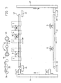
- Fig. 5 shows a schematic illustration of an embodiment of an apparatus for carrying out the method according to the invention.
- the device 10 has five processing stations 1 to 5, on which carrier devices 11 are guided successively and in the direction of the arrow.
- the carrier devices 11 are moved further from station to station by means of a conveyor belt 12 and are conveyed back to the beginning of the conveyor belt 12 after creation of the chip module with connected conductor loop and removal of the same from the carrier device via a lift 13, a return conveyor 14 and another lift 14, to be available for editing another module.
- the transition from the conveyor belts to the lifts is preferably achieved by means of sliding devices 15.
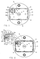
- FIGS. 1 to 4 illustrate a preferred embodiment of the carrier device according to the invention.
- Fig. 4 shows a cross section through the preferred embodiment for the carrier device.
- the carrier device consists of two parts, a holding part 16 and a Base part 17.
- the upper part of the support device, ie the holding part, is again shown in FIG. 3 and designated by the reference numeral 18.
- the holding part 18 can be lifted out of the base part during the processing of grippers and fed to nearby processing stations.
- the base part preferably remains on the conveyor belt during processing and, at the end of a machining operation, picks up the holding part again to be transported together with it to the next processing station.
- Fig. 1 shows a plan view of the preferred embodiment for the holding part 16.
- the preferred embodiment for the carrier device is suitable for producing conductor loops for use in contactless chip cards.
- Fig. 2 in which the holding part 16 is shown with finished wound conductor loop 19, in the preferred embodiment, a conductor loop shape is generated, which has similar dimensions as a standard chip card, so that the conductor loop after insertion into the card body close to the Edge of the card runs, thus enclosing a maximum area.
- FIG. 2 further shows a chip module 20 inserted into a trough of the carrier device, comprising a chip 21, which is encased by a protective layer 22, as well as contact surfaces 23a and 23b.
- the finished conductor loop 19 is welded at its two ends to the contact surfaces 23a and 23b. In this state, the chip module with attached conductor loop can be removed from the carrier device.
- the chip module 20 is held by means of a clamping device 24, consisting of two gripping arms which laterally contact the chip module.
- the gripping arms 24 hold the chip module by means of spring force, which is caused by a spring in the interior of the carrier device.
- the two grippers For insertion and removal of the chip module from the clamping device 24, the two grippers must be moved outwardly, which is effected by a preferably bolt-shaped actuator 25, as shown in Fig. 4, against the force of a spring 26 in the interior the holding part 17 of the carrier device is pressed.
- the thus pressed inwardly pin 25 engages in an opening 27 of a mandrel-shaped extension 28 of the holding part 18, in the interior of a preferably designed as a push rod transfer member is present, in turn, with the grippers of the clamping device 24 is in operative connection. Due to the penetration of the bolt 25 into the opening 26, the rod guided in the interior of the mandrel 28 is pulled down, which results in that the grippers of the clamping device 24 are moved outwards and thus an inserted chip module is released or space is created. to use a new chip module. When the pressure on the bolt 25 is removed, the grippers close again and hold an inserted new chip module.
- an actuation of the bolt 25 in two positions is possible.
- a first position the mentioned opening of the gripper of the clamping device 24 is effected.
- a lowering of an inner part 29 relative to an outer part 30 of the holding part 16 is effected. This reduction supports the removal of a finished conductor loop 19 of the holding part.
- winding supports or projections 31 are present on the holding part, over which the conductor loop is wound during winding and thus obtains the desired shape.
- the cross sections according to FIGS. 3 and 4 also show each one of the gripping arms of the clamping device 24 again.
- Figs. 1 to 4 mounting pins 32a and 32b are shown, which serve for attaching the conductor loop wire before and after the winding process
- deflection pins 33a and 32b are shown, which stretch as well as the winding posts 31, the conductor loop during winding.
- the mounting pins 32a and 32b each have a sharp edge, which facilitate a defined tearing of the conductor loop wire under a pulling movement.
- the winding of the conductor loop takes place as follows.
- the conductor loop is fed via a not shown tool from a conductor loop supply spool and fastened to a web of the corresponding processing station. Subsequently, the wire is guided to the fixing pin 32a and fixed there. The web at the processing station is now moved away from the mounting pin of the support device, causing the wire under train and at the edge 34th of the fastening pin 32a breaks off. The free end of the wire is now guided around the deflection pin 33a and laid from there in a clockwise direction along the winding supports 31. According to the later use of the chip module with attached conductor loop one or more, possibly up to several hundred windings can be achieved by rotating the holding member 16 in a winding device.
- the conductor loop wire is returned via the deflection pin 32 b in the interior of the holding device 16, fixed there on the further mounting pin 32 b and then fixed with a fastening web on the winding device, not shown.
- the conductor loop wire again comes under tension and tears at the edge 34 of the fastening pin 32b.
- a conductor loop having a plurality of windings has now been laid around the winding supports 31, and the free ends of the conductor loop wire lead to the covering pins 32a, 32b. Due to the orientation of the pins 32 and 33, the two free wire ends extend directly over the contact surfaces 23a and 23b of the chip module and can then be welded to these. Likewise, after welding, the free ends may be cut off and blown away by a blower device. For blowing away, the fastening pins 32a and 32b can preferably be lowered into the interior of the holding part 16 against a spring force. For this purpose, the mounting pins 32a and 32b on small wells, engage in the pins that press the mounting pins down.
- FIG. 5 schematically shows chip modules 35, which are strung together via a band 36 or form the band 36 by connection to one another.
- a chip module to be processed is punched out of the tape and brought by means of a gripper to the resting on the conveyor support device 11 and inserted into the trough in the holding part 16.
- To insert the bolt 25 must be pressed at the same time in the first position so that the clamping device 24 opens and the insertion of the chip module can be done at the same time.
- the carrier device 11 is moved on to the second processing station.
- the conductor loop is wound in this processing station.
- the holding part 16 of the carrier device is pulled out of the base part 17 by means of a gripper, which preferably engages in a taper 37, as shown in FIGS. 3 and 4.
- the holding part is tilted by 90 ° to be used with the mandrel-shaped end 28 in the winding device.
- the winding device has a in Fig. 5 schematically indicated rotor 38 which has two receiving portions 39 and 40 for simultaneously receiving two holding parts.
- a not yet wound holding part is brought into a position in which the winding takes place, and at the same time a finished wound holding part is returned to the position from which it is removed again by the gripper and returned to the base part can be. If a holding part 'is in the suitable position for winding after the 180 ° rotation of the rotor, then the holding element's mandrel 28 is coupled to an axis of rotation which allows the holding part to be rotated for winding.
- the conductor loop wire Before winding, the conductor loop wire is brought in and fixed to one of the fixing pins 32a by the above-described method. The winding and the re-attachment of the wire to the mounting pin 32b in the manner described above.
- the conductor loop wire preferably has a sheath which adheres to adjacent conductor loops under the influence of heat.
- a composite of a plurality of conductor loops is achieved, which can later be more easily removed from the carrier device and is better suited for subsequent processing steps.
- a heating device particularly preferably a heating nozzle, is preferably located on the winding device. Heating can only start during the rotation or starts a short time before.
- the holding member After the holding member has been wound, it is returned by the rotor by means of a 180 ° movement to the position where it can be removed by the gripper and reset in the base part. Subsequently, the carrier device is transported to the processing station 3. In the processing station 3, the two wire ends are firmly welded to the two contact surfaces 23a and 23b of the chip module. As explained with reference to FIGS. 1 and 2, the two wire ends extend due to their attachment to the mounting pins 32a and 32b directly above the contact surfaces. Thus, in a simple manner by bringing a welding device, a welding of the wire ends done with the corresponding contact surfaces. For welding, the holding part preferably remains in the base part, but can also be removed.
- the two ends of the wire loop which protrude from welding points are cut off.
- the cutting can be done by lifting the entire support device or only the holding part in the direction of an overlying cutting tool.
- the cut wire ends are preferably removed by means of a blower device.
- the fastening webs 32a and 32b can be lowered by means of pins brought up from above.
- the conductor loop with a connected chip module can be removed from the carrier device.
- the removal takes place by pressing the bolt 25 of FIG. 4 in the second position, ie in a position in which both the clamping device 24 opens and thus the module is released as well as the inner part 29 of the holding part itself lowers against the outer part 30.
- a gripping device approaches from above, which preferably engages in the conductor loop approximately at the points where the winding supports are located.
- the corresponding gripper preferably consists of two short and two long webs, which are respectively arranged along the short and long sides of the windings.
- a plurality of such chip module conductor loop units are preferably produced and placed side by side on the mentioned film. Such finished benefits can then be supplied to further processing steps, preferably further lamination steps.
- the inventive method is generally suitable for the production of units of chips with conductor loops for transponder applications.
- the conductor loop shape can be virtually any desired with the mentioned method and in particular be executed in any size.
- the specified manner of producing the windings, the carrier device itself, as well as the method and the device for removing the conductor loop from the carrier device represent independent inventive aspects.
- a combination of these individual elements with each other is advantageous, but not mandatory.
- the nature of the arrangement of the individual processing stations in the schematic shown in Fig. 5 is advantageous, but these processing stations can also be arranged along a circle or used individually.
- the winding device may comprise a rotor, at the two ends of which a carrier device can be used in each case and is brought into the position for winding via a 180 ° rotation of the rotor.
- the attachment of the wire may include the substeps of:
- the carrier device can be transported by a conveyor belt from one processing station to the next and be transported back after removal of the conductor loop with a connected chip or chip module from the carrier device to the first processing station.
- the support device may be made in two parts, with a base part always remains on the conveyor belt and a holding part with a clamping device, for individual processing steps, in particular during winding, is removed by grippers from the base part.
- the carrier device may include a tool identifier, by means of which the processing stations can differentiate carrier devices which are equipped with a chip or chip module from carrier devices which are empty.
- the working surface of the holding part of the device can have an inner and an outer part, wherein the inner part can be lowered relative to the outer part.
- the holding part of the device may have in its interior a transmission member, which is coupled to the actuating device of the base part and allows the actuating device to lower the inner part of the working surface.
- the inner part of the work surface may have approximately the dimensions of a standard chip card and arrange the winding posts along the edge of this lowerable inner region, wherein the winding posts are hook-shaped and dimensioned so that a wound around it conductor loop touches the work surface.
- the clamping device has two grippers, which comprise an inserted chip module from two sides and hold by spring force and increase their mutual distance upon actuation of the actuator of the base part to release the chip module.
- the carrier device may comprise two retractable mounting pins, to which the two ends of the conductor loop can be fastened during the winding process, wherein the fastening pins each have a sharp edge, in order to achieve a tearing of the conductor loop wire under tension.
- a method for removing the conductor loop from a carrier device may comprise the following steps: first actuating the actuator of the base member to achieve disengagement of the chip module from the clamp, second actuating the actuator of the base member to achieve lowering of the inner portion of the coiled conductor work surface, and removing the conductor loop from the support means and gripping means Placing the functional unit consisting of conductor loop and chip module on a foil. Furthermore, the removed functional unit chip module and conductor loop of an antenna can be supplied to perform a functional test.
- the chip module in the method can be provided with an adhesive on its underside before being placed on the film, the conductor loop being heated on the film before being placed on the film and placed under pressure on the film.
Landscapes
- Engineering & Computer Science (AREA)
- Computer Hardware Design (AREA)
- Microelectronics & Electronic Packaging (AREA)
- Physics & Mathematics (AREA)
- General Physics & Mathematics (AREA)
- Theoretical Computer Science (AREA)
- Credit Cards Or The Like (AREA)
- Coil Winding Methods And Apparatuses (AREA)
Claims (6)
- Procédé pour la fabrication d'une boucle conductrice (19) connectée à une puce (21) ou un module à puce (20), pour une utilisation dans les transpondeurs, de préférence avec des cartes à puce sans contact, d'après les étapes suivantes .A) Amenée d'une puce (21) ou d'un module à puce (20),B) Mise en place de la puce ou du module à puce dans un dispositif de support (16, 17, 18) mobile comprenant un dispositif de serrage (24) permettant de fixer le module à puce (20) sur le dispositif de support,C) Déplacement relatif du dispositif de support (16, 17, 18) vers un dispositif d'enroulement de la boucle conductrice,D) Mise en place d'au moins une partie du dispositif de support (18), tout en introduisant le dispositif de serrage (24) dans le dispositif d'enroulement,E) Amenée d'un fil de la boucle conductrice et fixation (32a) du fil sur la partie du dispositif de support (18) mise en place dans le dispositif d'enroulement,F) Rotation du dispositif de support (18) mis en place pour la réalisation d'une boucle conductrice composée de plusieurs enroulements, la forme de la boucle conductrice étant déterminée par des supports d'enroulement (31) placés au niveau du dispositif de support, afin de donner à la boucle conductrice une forme appropriée pour l'insertion dans un corps de transpondeur ou corps de carte,G) Fixation d'une extrémité libre du fil d'enroulement sur un autre point (32b) du dispositif de support,H) Séparation par découpe du fil enroulé autour du dispositif de support du fil de boucle conductrice restant,I) Déplacement relatif du dispositif de support vers un dispositif de mise en contact,J) Mise en contact des deux extrémités du fil avec des surfaces de contact correspondantes (23a, 23b) de la puce ou du module à puce,K) Retrait de la boucle conductrice (19) connectée à la puce (21) ou au module à puce (22), tout en libérant en même temps la puce ou le module à puce du dispositif de serrage,L) Application d'une couche d'adhésif sur la puce (21) ou le module à puce (20) et application de la boucle conductrice connectée à la puce ou au module à puce sur un film, la boucle conductrice étant chauffée préalablement à son application, et pressée intégralement ou partiellement dans le film.
- Procédé selon la revendication 1, caractérisé en ce que la boucle conductrice est enroulée, en forme de polygone à n sommets ou préférablement de rectangle, afin de s'étendre le long ou près des bords de la carte à puce.
- Procédé selon la revendication 1 ou 2,
caractérisé en ce que le fil de la boucle conductrice comporte une gaine isolante, qui colle aux couches isolantes des boucles adjacentes sous l'influence de la chaleur. - Procédé selon la revendication 3, caractérisé en ce que le fil de la boucle conductrice est chauffé, pendant ou avant l'étape F), de préférence au moyen d'une buse de chauffe.
- Procédé selon l'une des revendications précédentes, caractérisé en ce qu'un test de fonctionnement de l'unité électrique, composée de la boucle conductrice et de la puce ou du module à puce, est réalisé suite à l'étape K).
- Procédé selon la revendication 5, caractérisé en ce que la boucle conductrice connectée à la puce ou au module à puce est passée par un champ d'antenne pour l'exécution du test.
Applications Claiming Priority (2)
| Application Number | Priority Date | Filing Date | Title |
|---|---|---|---|
| DE19848009 | 1998-10-19 | ||
| DE19848009A DE19848009C2 (de) | 1998-10-19 | 1998-10-19 | Verfahren zum Herstellen einer Leiterschleife mit angeschlossenem Chipmodul zur Verwendung in kontaktlosen Chipkarten sowie Trägervorrichtung zur Verwendung in dem Verfahren sowie kontaktlose Chipkarte |
Publications (3)
| Publication Number | Publication Date |
|---|---|
| EP0996086A2 EP0996086A2 (fr) | 2000-04-26 |
| EP0996086A3 EP0996086A3 (fr) | 2000-06-28 |
| EP0996086B1 true EP0996086B1 (fr) | 2006-10-18 |
Family
ID=7884862
Family Applications (1)
| Application Number | Title | Priority Date | Filing Date |
|---|---|---|---|
| EP99115251A Expired - Lifetime EP0996086B1 (fr) | 1998-10-19 | 1999-08-02 | Procédé de fabrication d'une boucle conductrice connectée à un module comprenant une puce pour utilisation en tant que cartes à puce sans contact, ainsi qu'un dispositif de support à utiliser dans le procédé |
Country Status (4)
| Country | Link |
|---|---|
| EP (1) | EP0996086B1 (fr) |
| AT (1) | ATE343181T1 (fr) |
| DE (2) | DE19848009C2 (fr) |
| ES (1) | ES2275325T3 (fr) |
Families Citing this family (9)
| Publication number | Priority date | Publication date | Assignee | Title |
|---|---|---|---|---|
| DE10160390A1 (de) * | 2001-12-10 | 2003-06-18 | Cubit Electronics Gmbh | Spulenanordnung und Verfahren zu ihrer Herstellung |
| DE102004010013B4 (de) * | 2003-03-05 | 2006-10-12 | Pav Card Gmbh | Verfahren zum Kontaktieren eines Chipmoduls |
| DE102009022427A1 (de) * | 2009-05-22 | 2010-11-25 | Melzer Maschinenbau Gmbh | Verfahren und Einrichtung zum Wickeln und Verlegen einer Spule |
| CN110524889B (zh) * | 2019-08-08 | 2024-07-19 | 广州明森合兴科技有限公司 | 一种非接触智能卡制造设备的定位系统 |
| IT202100021722A1 (it) * | 2021-08-11 | 2023-02-11 | Gd Spa | Metodo e macchina per realizzare una bobina attorno ad un componente di un articolo |
| EP4374289A1 (fr) * | 2021-07-23 | 2024-05-29 | G.D Societa' Per Azioni | Procédé et machine pour fabriquer une bobine autour d'un composant d'un article |
| IT202100027428A1 (it) * | 2021-10-26 | 2023-04-26 | Gd Spa | Metodo e macchina per realizzare una bobina attorno ad un componente di un articolo |
| IT202100027422A1 (it) | 2021-10-26 | 2023-04-26 | Gd Spa | Metodo e macchina per realizzare una bobina attorno ad un componente di un articolo |
| CN115084050B (zh) * | 2022-07-25 | 2022-11-11 | 成都汉芯国科集成技术有限公司 | 一种采用BGA接口的宽带射频系统级sip封装结构 |
Citations (1)
| Publication number | Priority date | Publication date | Assignee | Title |
|---|---|---|---|---|
| DE19710656A1 (de) * | 1997-03-14 | 1998-09-17 | Fd Fleischhauer Datentraeger U | Chipkarte |
Family Cites Families (8)
| Publication number | Priority date | Publication date | Assignee | Title |
|---|---|---|---|---|
| FR2593320B1 (fr) * | 1986-01-21 | 1988-03-04 | Europ Composants Electron | Procede de fabrication d'un composant inductif pour report a plat |
| EP0526484B1 (fr) * | 1990-04-19 | 1994-03-16 | GUSTAFSON, Ake | Procede d'assemblage d'une bobine sur un circuit imprime |
| US5115560A (en) * | 1991-10-03 | 1992-05-26 | Amp Incorporated | Terminal insertion apparatus having improved turntable assembly |
| DE4220194C2 (de) * | 1992-06-19 | 1996-02-22 | Herbert Stowasser | Vorrichtung und Verfahren zur Herstellung eines Transponders, wobei Wickeldraht einer Spule mit den Anschlußflächen eines elektronischen Bauelementes (Chip) verbunden wird |
| DE4307064C2 (de) * | 1993-03-06 | 1996-04-25 | Amatech Gmbh & Co Kg | Verfahren und Vorrichtung zur Herstellung einer Anordnung aus einem elektronischen Bauelement und einer gewickelten Spule |
| DE4408124C2 (de) * | 1994-03-10 | 1998-03-26 | Amatech Gmbh & Co Kg | Verfahren und Vorrichtung zur Herstellung einer Anordnung aus mindestens einem elektronischen Bauelement (IC) und einer gewickelten Spule |
| DE19634661A1 (de) * | 1996-08-28 | 1998-03-05 | David Finn | Verfahren und Vorrichtung zur Herstellung einer Spulenanordnung |
| EP0937304A1 (fr) * | 1996-11-11 | 1999-08-25 | Metget AB | Procede de fabrication et de fixation de bobines et appareil de realisation de ce procede |
-
1998
- 1998-10-19 DE DE19848009A patent/DE19848009C2/de not_active Expired - Fee Related
-
1999
- 1999-08-02 EP EP99115251A patent/EP0996086B1/fr not_active Expired - Lifetime
- 1999-08-02 DE DE59913928T patent/DE59913928D1/de not_active Expired - Lifetime
- 1999-08-02 ES ES99115251T patent/ES2275325T3/es not_active Expired - Lifetime
- 1999-08-02 AT AT99115251T patent/ATE343181T1/de not_active IP Right Cessation
Patent Citations (1)
| Publication number | Priority date | Publication date | Assignee | Title |
|---|---|---|---|---|
| DE19710656A1 (de) * | 1997-03-14 | 1998-09-17 | Fd Fleischhauer Datentraeger U | Chipkarte |
Also Published As
| Publication number | Publication date |
|---|---|
| ES2275325T3 (es) | 2007-06-01 |
| EP0996086A2 (fr) | 2000-04-26 |
| DE19848009C2 (de) | 2001-10-04 |
| EP0996086A3 (fr) | 2000-06-28 |
| DE19848009A1 (de) | 2000-04-27 |
| DE59913928D1 (de) | 2006-11-30 |
| ATE343181T1 (de) | 2006-11-15 |
Similar Documents
| Publication | Publication Date | Title |
|---|---|---|
| DE4301234B4 (de) | Verfahren und Einrichtung zum Herstellen von Ankern für elektrodynamische Maschinen | |
| EP3828967B1 (fr) | Procédé de fabrication d'un empilement d'électrodes pour l'accumulateur d'énergie, installation d'empilement | |
| EP0689164A2 (fr) | Méthode de fabrication de parteurs d'information | |
| DE1465444A1 (de) | Gewebte elektronische Schaltung | |
| DE19509999C2 (de) | Verfahren und Vorrichtung zur Herstellung einer Transpondereinheit sowie Transpondereinheit | |
| EP0700575B1 (fr) | Tete de bobine | |
| EP1269496A1 (fr) | Procede pour produire une etiquette ou une carte a puce, dispositif pour mettre en oeuvre ledit procede, et etiquette ou carte a puce ainsi obtenue | |
| EP0996086B1 (fr) | Procédé de fabrication d'une boucle conductrice connectée à un module comprenant une puce pour utilisation en tant que cartes à puce sans contact, ainsi qu'un dispositif de support à utiliser dans le procédé | |
| DE3232859A1 (de) | Vorrichtung fuer den zusammenbau von mikrobauelementen | |
| DE10014620A1 (de) | Verfahren zur Herstellung eines Trägerbandes mit einer Vielzahl von elektrischen Einheiten, jeweils aufweisend einen Chip und Kontaktelemente | |
| DE4220194C2 (de) | Vorrichtung und Verfahren zur Herstellung eines Transponders, wobei Wickeldraht einer Spule mit den Anschlußflächen eines elektronischen Bauelementes (Chip) verbunden wird | |
| DE202020005420U1 (de) | Verarbeitungseinheit zum Einsetzen von elektronischen Vorrichtungen, die zur Hochfrequenzkommunikation geeignet sind, in entsprechende Kautschukhülsen | |
| EP0762323B1 (fr) | Procédé et dispositif pur la fabrication d'un élément de bobine pour un support de données à circuit intégré et couplage sans contact | |
| DE69703720T2 (de) | Vorrichtung zur Herstellung von Kabelbäumen | |
| DE10035638A1 (de) | Verfahren zum Herstellen eines elektrisch leitenden Musters auf einem Substrat | |
| WO1993009551A1 (fr) | Transpondeur ainsi que procede et dispositif pour sa fabrication | |
| WO2002056657A1 (fr) | Procede et dispositif pour placer des fils conducteurs sur ou dans une couche de support | |
| EP1856729A1 (fr) | Procede pour etablir une liaison electrique et mecanique entre des pastilles de puce et des pastilles d'antenne et transpondeur | |
| DE69207622T2 (de) | Vorrichtung zur Herstellung von in leitender Folie gewickelten elektronischen Bauteilen | |
| DE3640210C2 (fr) | ||
| EP0836372A2 (fr) | Méthode et appareil de création d'une surface d'aspiration sur un objet et composant électrique fabriqué ainsi | |
| DE19920399C1 (de) | Verfahren und Vorrichtung zur Herstellung von Leiterdrähten auf oder in einer elektrisch isolierenden Schicht | |
| DE2628519C3 (de) | Verfahren und Vorrichtung zur Herstellung der aus Drähten bestehenden Verbindungen zwischen den Anschlußstellen eines Bauelementes und Anschluß- oder Kontaktelementen | |
| DE19804877A1 (de) | Verfahren und Vorrichtung zum Kontaktieren von plattenförmigen Solarzellen | |
| DE102007037167A1 (de) | Einlagige Flachspule auf Substrat |
Legal Events
| Date | Code | Title | Description |
|---|---|---|---|
| PUAI | Public reference made under article 153(3) epc to a published international application that has entered the european phase |
Free format text: ORIGINAL CODE: 0009012 |
|
| AK | Designated contracting states |
Kind code of ref document: A2 Designated state(s): AT BE CH CY DE DK ES FI FR GB GR IE IT LI LU MC NL PT SE |
|
| AX | Request for extension of the european patent |
Free format text: AL;LT;LV;MK;RO;SI |
|
| PUAL | Search report despatched |
Free format text: ORIGINAL CODE: 0009013 |
|
| RIC1 | Information provided on ipc code assigned before grant |
Free format text: 7G 06K 19/077 A, 7H 01F 41/10 B, 7H 01F 41/06 B |
|
| AK | Designated contracting states |
Kind code of ref document: A3 Designated state(s): AT BE CH CY DE DK ES FI FR GB GR IE IT LI LU MC NL PT SE |
|
| AX | Request for extension of the european patent |
Free format text: AL;LT;LV;MK;RO;SI |
|
| 17P | Request for examination filed |
Effective date: 20001219 |
|
| AKX | Designation fees paid |
Free format text: AT BE CH CY DE DK ES FI FR GB GR IE IT LI LU MC NL PT SE |
|
| RAP1 | Party data changed (applicant data changed or rights of an application transferred) |
Owner name: GEMPLUS GMBH |
|
| GRAP | Despatch of communication of intention to grant a patent |
Free format text: ORIGINAL CODE: EPIDOSNIGR1 |
|
| GRAS | Grant fee paid |
Free format text: ORIGINAL CODE: EPIDOSNIGR3 |
|
| GRAA | (expected) grant |
Free format text: ORIGINAL CODE: 0009210 |
|
| AK | Designated contracting states |
Kind code of ref document: B1 Designated state(s): AT BE CH CY DE DK ES FI FR GB GR IE IT LI LU MC NL PT SE |
|
| PG25 | Lapsed in a contracting state [announced via postgrant information from national office to epo] |
Ref country code: NL Free format text: LAPSE BECAUSE OF FAILURE TO SUBMIT A TRANSLATION OF THE DESCRIPTION OR TO PAY THE FEE WITHIN THE PRESCRIBED TIME-LIMIT Effective date: 20061018 Ref country code: IE Free format text: LAPSE BECAUSE OF FAILURE TO SUBMIT A TRANSLATION OF THE DESCRIPTION OR TO PAY THE FEE WITHIN THE PRESCRIBED TIME-LIMIT Effective date: 20061018 Ref country code: FI Free format text: LAPSE BECAUSE OF FAILURE TO SUBMIT A TRANSLATION OF THE DESCRIPTION OR TO PAY THE FEE WITHIN THE PRESCRIBED TIME-LIMIT Effective date: 20061018 |
|
| REG | Reference to a national code |
Ref country code: GB Ref legal event code: FG4D Free format text: NOT ENGLISH |
|
| REG | Reference to a national code |
Ref country code: IE Ref legal event code: FG4D Free format text: LANGUAGE OF EP DOCUMENT: GERMAN Ref country code: CH Ref legal event code: EP |
|
| REF | Corresponds to: |
Ref document number: 59913928 Country of ref document: DE Date of ref document: 20061130 Kind code of ref document: P |
|
| PG25 | Lapsed in a contracting state [announced via postgrant information from national office to epo] |
Ref country code: SE Free format text: LAPSE BECAUSE OF FAILURE TO SUBMIT A TRANSLATION OF THE DESCRIPTION OR TO PAY THE FEE WITHIN THE PRESCRIBED TIME-LIMIT Effective date: 20070118 Ref country code: DK Free format text: LAPSE BECAUSE OF FAILURE TO SUBMIT A TRANSLATION OF THE DESCRIPTION OR TO PAY THE FEE WITHIN THE PRESCRIBED TIME-LIMIT Effective date: 20070118 |
|
| GBT | Gb: translation of ep patent filed (gb section 77(6)(a)/1977) |
Effective date: 20070122 |
|
| PG25 | Lapsed in a contracting state [announced via postgrant information from national office to epo] |
Ref country code: PT Free format text: LAPSE BECAUSE OF FAILURE TO SUBMIT A TRANSLATION OF THE DESCRIPTION OR TO PAY THE FEE WITHIN THE PRESCRIBED TIME-LIMIT Effective date: 20070319 |
|
| NLV1 | Nl: lapsed or annulled due to failure to fulfill the requirements of art. 29p and 29m of the patents act | ||
| ET | Fr: translation filed | ||
| REG | Reference to a national code |
Ref country code: IE Ref legal event code: FD4D |
|
| REG | Reference to a national code |
Ref country code: ES Ref legal event code: FG2A Ref document number: 2275325 Country of ref document: ES Kind code of ref document: T3 |
|
| PLBE | No opposition filed within time limit |
Free format text: ORIGINAL CODE: 0009261 |
|
| STAA | Information on the status of an ep patent application or granted ep patent |
Free format text: STATUS: NO OPPOSITION FILED WITHIN TIME LIMIT |
|
| 26N | No opposition filed |
Effective date: 20070719 |
|
| BERE | Be: lapsed |
Owner name: GEMPLUS G.M.B.H. Effective date: 20070831 |
|
| REG | Reference to a national code |
Ref country code: CH Ref legal event code: PL |
|
| PG25 | Lapsed in a contracting state [announced via postgrant information from national office to epo] |
Ref country code: MC Free format text: LAPSE BECAUSE OF NON-PAYMENT OF DUE FEES Effective date: 20070831 Ref country code: LI Free format text: LAPSE BECAUSE OF NON-PAYMENT OF DUE FEES Effective date: 20070831 Ref country code: GR Free format text: LAPSE BECAUSE OF FAILURE TO SUBMIT A TRANSLATION OF THE DESCRIPTION OR TO PAY THE FEE WITHIN THE PRESCRIBED TIME-LIMIT Effective date: 20070119 Ref country code: CH Free format text: LAPSE BECAUSE OF NON-PAYMENT OF DUE FEES Effective date: 20070831 |
|
| PG25 | Lapsed in a contracting state [announced via postgrant information from national office to epo] |
Ref country code: BE Free format text: LAPSE BECAUSE OF NON-PAYMENT OF DUE FEES Effective date: 20070831 |
|
| PG25 | Lapsed in a contracting state [announced via postgrant information from national office to epo] |
Ref country code: AT Free format text: LAPSE BECAUSE OF NON-PAYMENT OF DUE FEES Effective date: 20070802 |
|
| PG25 | Lapsed in a contracting state [announced via postgrant information from national office to epo] |
Ref country code: LU Free format text: LAPSE BECAUSE OF NON-PAYMENT OF DUE FEES Effective date: 20070802 Ref country code: CY Free format text: LAPSE BECAUSE OF FAILURE TO SUBMIT A TRANSLATION OF THE DESCRIPTION OR TO PAY THE FEE WITHIN THE PRESCRIBED TIME-LIMIT Effective date: 20061018 |
|
| PGFP | Annual fee paid to national office [announced via postgrant information from national office to epo] |
Ref country code: FR Payment date: 20110902 Year of fee payment: 13 Ref country code: ES Payment date: 20110805 Year of fee payment: 13 Ref country code: DE Payment date: 20110803 Year of fee payment: 13 Ref country code: GB Payment date: 20110728 Year of fee payment: 13 |
|
| PGFP | Annual fee paid to national office [announced via postgrant information from national office to epo] |
Ref country code: IT Payment date: 20110723 Year of fee payment: 13 |
|
| GBPC | Gb: european patent ceased through non-payment of renewal fee |
Effective date: 20120802 |
|
| REG | Reference to a national code |
Ref country code: FR Ref legal event code: ST Effective date: 20130430 |
|
| PG25 | Lapsed in a contracting state [announced via postgrant information from national office to epo] |
Ref country code: IT Free format text: LAPSE BECAUSE OF NON-PAYMENT OF DUE FEES Effective date: 20120802 |
|
| PG25 | Lapsed in a contracting state [announced via postgrant information from national office to epo] |
Ref country code: DE Free format text: LAPSE BECAUSE OF NON-PAYMENT OF DUE FEES Effective date: 20130301 Ref country code: GB Free format text: LAPSE BECAUSE OF NON-PAYMENT OF DUE FEES Effective date: 20120802 |
|
| PG25 | Lapsed in a contracting state [announced via postgrant information from national office to epo] |
Ref country code: FR Free format text: LAPSE BECAUSE OF NON-PAYMENT OF DUE FEES Effective date: 20120831 |
|
| REG | Reference to a national code |
Ref country code: DE Ref legal event code: R119 Ref document number: 59913928 Country of ref document: DE Effective date: 20130301 |
|
| REG | Reference to a national code |
Ref country code: ES Ref legal event code: FD2A Effective date: 20131018 |
|
| PG25 | Lapsed in a contracting state [announced via postgrant information from national office to epo] |
Ref country code: ES Free format text: LAPSE BECAUSE OF NON-PAYMENT OF DUE FEES Effective date: 20120803 |