EP0762323B1 - Procédé et dispositif pur la fabrication d'un élément de bobine pour un support de données à circuit intégré et couplage sans contact - Google Patents
Procédé et dispositif pur la fabrication d'un élément de bobine pour un support de données à circuit intégré et couplage sans contact Download PDFInfo
- Publication number
- EP0762323B1 EP0762323B1 EP96112883A EP96112883A EP0762323B1 EP 0762323 B1 EP0762323 B1 EP 0762323B1 EP 96112883 A EP96112883 A EP 96112883A EP 96112883 A EP96112883 A EP 96112883A EP 0762323 B1 EP0762323 B1 EP 0762323B1
- Authority
- EP
- European Patent Office
- Prior art keywords
- carrier
- wire
- coil
- winding
- wound
- Prior art date
- Legal status (The legal status is an assumption and is not a legal conclusion. Google has not performed a legal analysis and makes no representation as to the accuracy of the status listed.)
- Expired - Lifetime
Links
Images


Classifications
-
- G—PHYSICS
- G06—COMPUTING; CALCULATING OR COUNTING
- G06K—GRAPHICAL DATA READING; PRESENTATION OF DATA; RECORD CARRIERS; HANDLING RECORD CARRIERS
- G06K19/00—Record carriers for use with machines and with at least a part designed to carry digital markings
- G06K19/06—Record carriers for use with machines and with at least a part designed to carry digital markings characterised by the kind of the digital marking, e.g. shape, nature, code
- G06K19/067—Record carriers with conductive marks, printed circuits or semiconductor circuit elements, e.g. credit or identity cards also with resonating or responding marks without active components
- G06K19/07—Record carriers with conductive marks, printed circuits or semiconductor circuit elements, e.g. credit or identity cards also with resonating or responding marks without active components with integrated circuit chips
- G06K19/077—Constructional details, e.g. mounting of circuits in the carrier
- G06K19/07745—Mounting details of integrated circuit chips
- G06K19/07747—Mounting details of integrated circuit chips at least one of the integrated circuit chips being mounted as a module
-
- G—PHYSICS
- G06—COMPUTING; CALCULATING OR COUNTING
- G06K—GRAPHICAL DATA READING; PRESENTATION OF DATA; RECORD CARRIERS; HANDLING RECORD CARRIERS
- G06K19/00—Record carriers for use with machines and with at least a part designed to carry digital markings
- G06K19/06—Record carriers for use with machines and with at least a part designed to carry digital markings characterised by the kind of the digital marking, e.g. shape, nature, code
- G06K19/067—Record carriers with conductive marks, printed circuits or semiconductor circuit elements, e.g. credit or identity cards also with resonating or responding marks without active components
- G06K19/07—Record carriers with conductive marks, printed circuits or semiconductor circuit elements, e.g. credit or identity cards also with resonating or responding marks without active components with integrated circuit chips
- G06K19/077—Constructional details, e.g. mounting of circuits in the carrier
- G06K19/07749—Constructional details, e.g. mounting of circuits in the carrier the record carrier being capable of non-contact communication, e.g. constructional details of the antenna of a non-contact smart card
- G06K19/0775—Constructional details, e.g. mounting of circuits in the carrier the record carrier being capable of non-contact communication, e.g. constructional details of the antenna of a non-contact smart card arrangements for connecting the integrated circuit to the antenna
-
- G—PHYSICS
- G06—COMPUTING; CALCULATING OR COUNTING
- G06K—GRAPHICAL DATA READING; PRESENTATION OF DATA; RECORD CARRIERS; HANDLING RECORD CARRIERS
- G06K19/00—Record carriers for use with machines and with at least a part designed to carry digital markings
- G06K19/06—Record carriers for use with machines and with at least a part designed to carry digital markings characterised by the kind of the digital marking, e.g. shape, nature, code
- G06K19/067—Record carriers with conductive marks, printed circuits or semiconductor circuit elements, e.g. credit or identity cards also with resonating or responding marks without active components
- G06K19/07—Record carriers with conductive marks, printed circuits or semiconductor circuit elements, e.g. credit or identity cards also with resonating or responding marks without active components with integrated circuit chips
- G06K19/077—Constructional details, e.g. mounting of circuits in the carrier
- G06K19/07749—Constructional details, e.g. mounting of circuits in the carrier the record carrier being capable of non-contact communication, e.g. constructional details of the antenna of a non-contact smart card
- G06K19/07773—Antenna details
- G06K19/07777—Antenna details the antenna being of the inductive type
- G06K19/07779—Antenna details the antenna being of the inductive type the inductive antenna being a coil
- G06K19/07781—Antenna details the antenna being of the inductive type the inductive antenna being a coil the coil being fabricated in a winding process
-
- H—ELECTRICITY
- H01—ELECTRIC ELEMENTS
- H01L—SEMICONDUCTOR DEVICES NOT COVERED BY CLASS H10
- H01L2924/00—Indexing scheme for arrangements or methods for connecting or disconnecting semiconductor or solid-state bodies as covered by H01L24/00
- H01L2924/0001—Technical content checked by a classifier
- H01L2924/0002—Not covered by any one of groups H01L24/00, H01L24/00 and H01L2224/00
Definitions
- the invention relates to a coil element for a Media with integrated circuit and non-contact Coupling, especially an IC card, and a Method for producing such a coil element.
- IC cards are used in different areas used, for example as telephone cards, Credit cards, check cards, ID cards, etc.
- An IC card usually has a contact field via which an IC embedded in the card with a external device for data processing coupled can be.
- the device has Data processing a corresponding counterpart to Contact field of the IC card on, if necessary with the Contact field are brought into a conductive connection can.
- IC cards are also known which are used instead of Contact field or in addition to the contact field Have coil. With the help of this coil is one non-contact data and energy transfer between the IC card and the data processing device possible by means of electromagnetic radiation.
- the sink is in during the manufacturing process of the IC card embedded the card body. They are different Method known an IC card with a coil equip.
- EP 0 640 940 A2 describes a coil element for a data carrier with a integrated circuit known that a wire coil with several, wraps wrapped using a varnish.
- the coil stiffened in this way can be manufactured separately and with conventional ones Tools are handled.
- the coil stiffening makes it easier in practice especially transportation.
- the insertion of the coils in data carriers remains difficult, however, because the coil ends are fragile and their connection to the integrated circuit is complex.
- EP 0 481776 A2 also discloses a TAB film Carrier element for producing a contactless IC card, on which the printed circuit structures of the card are produced using printing technology are.
- the conductor track structure includes a multi-turn structure Coil structure. A difficulty with such printed spools forms the formation of sufficiently powerful coils. The production printed spools is also comparatively expensive.
- EP 0689164A2 which is relevant only in accordance with Article 54 (3) EPC a method for producing a data carrier with non-contact Coupling known, after that by means of a conically shaped winding body First a wire shape with a 3-dimensional structure is produced is then stripped off on a film and pressed together becomes. When pressed together, a flat coil is created.
- the invention has for its object to be as inexpensive as possible and largely automated production of data carriers with integrated circuit and non-contact coupling, meet the high quality requirements.
- the basic principle of the invention is that for the production of data carriers that can be operated without contact, no loose wire-wound coils are used, but coil elements in which a wire-wound Coil on a support for mechanical stabilization of the coil, for example attached to a film, which is hereinafter referred to as a carrier film is.
- a carrier film When manufacturing the coil elements, the coils become direct wrapped on the carrier as a base, one after the winding process removable winding core gives the coil the desired shape.
- the Coil elements can optionally already have an IC have at the ends of the wire-wound coil is contacted.
- the coil elements can both manufactured individually and to data carriers be processed as well as in the form of a Multi-purpose sheet on a common carrier has several wire-wound coils.
- the disk can be manufactured entirely in multi-use production and be separated at the end from the multiple-use sheet or else also from the beginning in one-off production or it can be made with start a multi-use production and during of the manufacturing process can be the multiple-use sheet be divided and continued with individual production become.
- the disk can be manufactured entirely in multi-use production and be separated at the end from the multiple-use sheet or else also from the beginning in one-off production or it can be made with start a multi-use production and during of the manufacturing process can be the multiple-use sheet be divided and continued with individual production become.
- the task is performed by those in the sibling Features specified resolved.
- the invention has the advantage that it is efficient and inexpensive manufacture of contactless operable IC cards or similar data carriers allows because the difficult handling of the sensitive wire spools and the elaborate Positioning work of the wire coils on the substrate eliminated. Another advantage of the invention is in that a multi-use production of the coil elements is possible and thus the manufacturing process becomes more efficient. Furthermore, the invention has the Advantage that the coil is very precisely in the card body can be positioned. An exact positioning of the Coil is particularly important if the Card body is then embossed, because then it must be ensured that in the embossing area no turns. Otherwise it would Embossing quality are impaired and there would be Risk of the turns being interrupted by the embossing become.
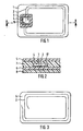
- the Dimensions of the card body 1 can according to the ISO standard 7810.
- the card body 1 contains one wire-wound coil 2 and a chip module 3, which in a recess 4 is arranged.
- the IC card can it’s a phone card, ID card, one Trade check card, credit card, or the like.
- the chip module 3 does not contain one explicitly in FIG. 1 illustrated IC, the contact surfaces 16 of the Chip module 3 is electrically connected.
- the Contact surfaces 16 are still with the two ends the wire-wound coil 2 connected.
- Is over the wire wound coil 2 a data exchange with an external Data processing device possible.
- the data transfer between the IC card and the external Data processing device takes place by means of electromagnetic radiation.
- the energy supply of the IC card is usually provided by the external Data processing device emitted electromagnetic Radiation ensured.
- the card body 1 has an upper cover film 5 and a lower cover film 8 on. Under the top cover film 5 is a substrate film 7 arranged which a recess 4 for receiving the Has chip module 3.
- the substrate film 7 follows a carrier film 6 and the wire-wound coil 2 existing coil element.
- the Card body the chip module 3, which is on the coil element is fixed with a casting compound 17.
- the wire ends of the Coil 2 are for contacting the contact surfaces 16 passed over the chip module 3.
- cover films 5 and 8 can be omitted, for example or additional foils can be added.
- the number and the order of the foils used, their thickness and the material used can vary.
- injection-mold the card body 1 manufacture the coil element in a Injection mold can be placed and either one-sided or be provided with injection molding compound on both sides.
- Fig. 3 shows a coil element consisting of a Carrier film 6 and one fixed thereon wire-wound coil 2.
- the coil 2 can by means of a Adhesive, for example, thermally or by pressure can be activated, can be fixed on the carrier film 6. This fixation makes the sensitive coil 2 protected against accidental deformation.
- the Coil element has a higher mechanical stability than a loose spool and also a bigger one Attack surface, so that the mechanical handling of the Coil element is simpler than that of a loose coil.
- Fig. 4 shows a coil element in which in addition to Carrier film 6 and a wire-wound coil 2 Chip module 3 is provided.
- the chip module 3 can, as in Fig. 4 can be arranged above the coil 2, wherein the wire ends of the coil 2 to the contact surfaces 16 of the Chip module 3 are pulled up and is by means of a suitable adhesive with the coil 2 and / or Carrier film 6 connected.
- the exemplary embodiment shown could be the chip module 3 also between the coil 2 and the carrier film 6 be attached or on the back of the carrier film 6. In the latter case, the contacting between the chip module 3 and the coil through holes take place in the carrier film 6.
- the structure of the chip module 3 is known per se.
- the chip module 3 contains one integrated circuit using bond wires with at least two contact surfaces 16 of the chip module 3 connected is.
- the contact surfaces 16 of the chip module 3 are also connected to the ends of the wire wound coil 2 connected.
- the coil element shown in Fig. 4 in principle already provides a fully functional IC card
- the lamination of further layers or the Spraying more material than if necessary further processing steps in the manufacture of a IC card from the coil element mainly serve the desired external dimensions of the IC card to achieve adequate mechanical durability ensure the required of the card Security requirements and the card visually to make it appealing.
- Fig. 5 shows a multiple-use sheet, in which several wire-wound coils 2 on a common Carrier film 6 are arranged.
- the multi-use sheet contains coil elements according to FIG. 3 or according to Fig. 4.
- Multi-purpose sheet consisting of a variety of Coil elements exist to manufacture IC cards throughout in multi-use production.
- Processing steps carried out on the complete sheet and only at the end of the manufacturing process individual IC cards divided out of the sheet. Thereby the manufacturing process can be very efficient design because with every processing step several pieces can be processed at the same time.
- the carrier film 2 is applied to a mounting plate 9. Liability the carrier film on the receiving plate 9 can for example by creating a vacuum between the carrier film 6 and the receiving plate 9 causes become.
- the winding cores 10 are by means of a generated by the receiving plate 9 Magnetic field held in place. Through this The type of bracket can damage the carrier film 6 can be avoided and there is enough space for that Winding the coils 2.
- FIG. 7 is an enlarged section of that in FIG. 6 shown device shown in cross section.
- Fig. 7 shows one of the winding cores 10, the by means of a arranged in the receiving plate 9 Electromagnets 14 against those on the mounting plate 9 overlying carrier film 6 is pressed.
- the winding core 10 is shaped so that it together with that on the Support plate 9 overlying carrier film 6 as Abutment forms an annular gap in which the Wire 13 can be wound.
- the feeding of the Wire 13 to the annular gap is made by means of Wire guide 11.
- the Wire guide 11 led around the annular gap or it is caused by an eccentric movement of the Mounting plate 9 of the annular gap in a corresponding Way around the wire guide 11. In both Cases arise in the annular gap wire wound coil 2.
- the carrier film 6 is placed on the receiving plate 9 applied and by applying a vacuum between the carrier film 6 and the surface of the receiving plate 9 fixed.
- the negative pressure can be generated that through channels not shown in the figure Mounting plate 9 air is pumped out.
- the winding cores 10 with a positioning device desired positions of the carrier film 6 arranged.
- the Positioning device can, for example, gripping arms Inclusion of the winding cores 10 included.
- the winding cores 10 can also by negative pressure or by means Electromagnet held by the positioning device become.
- the Wires 13 by means of the wire guides 11 to the Winding cores 10 brought up and according to known The wire ends are moved into the winding cores 10 threaded.
- the wires 13 are provided with a fixing compound which the individual turns of the coils 2 with each other connects and the coils 2 on the carrier film 6th fixed.
- the fixing compound can also on the Carrier film 6 are applied to the Places where the coils 2 are positioned.
- the fixing compound in the area of the coils 2 either applied over the entire surface or only partially become.
- the setting compound can be cured by pressure, by ultrasound, by raising the temperature or by Irradiation with ultraviolet light can be favored. This can increase the temperature, for example generated that you can an electrical current through the coils 2 can flow.
- the wires 13 severed and the winding cores 10 are of the Carrier film 6 removed so that on the carrier film wire-wound coils 2 remain.
- the removal the winding cores 10 is facilitated in that they a non-stick coating, for example Teflon, are provided, the adhesion of the fixing compound to the Winding cores prevented.
- the carrier film 6 including those fixed thereon wire-wound coils 2 from the mounting plate 9 would be removed and sent for further processing become.
- This further processing can either take place on the from the carrier film and the coils located thereon 2 formed multipurpose sheets are carried out or this multi-use sheet can be divided into individual coil elements be divided, each from a wire wound coil 2 and a section of the Carrier film 6 exist.
- each winding core 10 there is a recess in each winding core 10 provided that a chip module 3 can accommodate.
- each winding core has 10 wire guide devices in which the wire ends of the coil 2 are inserted can and so the provided on the chip module 3 Contact surfaces 16 supplied and electrically with them can be conductively connected.
- the coils 2 not during the wrapping process Carrier film 6 applied, but initially completely wound on the winding cores 10 and then on transfer the carrier film 6. The transfer takes place directly from the winding cores 10 to the carrier film 6, so that handling loose coils 2 is not is required.
- the Winding cores 10 to be slightly modified in shape slipping of the turns from the winding cores 10 to prevent or this slipping can otherwise - for example by a removable lock - prevented become.
Landscapes
- Engineering & Computer Science (AREA)
- Microelectronics & Electronic Packaging (AREA)
- Computer Hardware Design (AREA)
- Physics & Mathematics (AREA)
- General Physics & Mathematics (AREA)
- Theoretical Computer Science (AREA)
- Computer Networks & Wireless Communication (AREA)
- Credit Cards Or The Like (AREA)
Claims (15)
- Procédé de fabrication d'éléments de bobine pour un support de données avec un circuit intégré et à couplage sans contact, caractérisé en ce qu'on réalise le bobinage d'au moins une bobine (2) sur un support (6) servant de base avec utilisation d'un noyau de bobine susceptible d'être enlevé et ou fixe la bobine (2) sur le support (6) pendant ou immédiatement après le processus de bobinage,.
- Procédé selon la revendication 1, caractérisé en ce que le support (6) est fixé de façon détachable sur la plaque de réception (9) et en ce qu'au moins un corps de bobinage (10) est positionné sur le support (6).
- Procédé selon la revendication 2, caractérisé en ce que le support (6) est fixé de façon détachable par l'application d'une dépression entre le support (6) et la plaque de réception (9).
- Procédé selon la revendication 2 ou 3, caractérisé en ce que le ou les corps de bobinage (10) est/sont maintenu(s) au moyen d'un champ magnétique créé par la plaque de réception (9).
- Procédé selon l'une des revendications 2 à 4, caractérisé en ce que l'on amène sur chaque corps de bobinage (10) un fil (13) au moyen d'un guidage de fil (11) et on réalise le bobinage d'une bobine (2) par déplacement excentrique de la plaque de réception (9) ou par déplacement correspondant du guidage de fil (11) sur chaque corps de bobinage (10).
- Procédé selon l'une des revendications 2 à 5, caractérisé en ce que l'on éloigne le corps de bobinage (10), du support (6) après la fin du processus de bobinage (6), les bobines (2) embobinées restant sur le support (6).
- Procédé selon l'une des revendications 2 à 5, caractérisé en ce que les bobines embobinées (2) sont fixées sur le support (6) au moyen d'une masse de fixation (17) qui est appliquée sur le support (6) avant le processus de bobinage ou qui est amenée aux fils (13) pendant le processus de bobinage.
- Procédé selon l'une des revendications 2 à 7, caractérisé en ce que les extrémités de fils de chaque bobine embobinée (2) sont amenées en contact avec un module de puce (3).
- Dispositif pour fabriquer des éléments de bobine pour un support de données avec un circuit intégré et à couplage sans contact, caractérisé en ce qu'il comporte : une plaque de réception (9) pour recevoir un support (6) pour la stabilisation mécanique de bobines embobinées (2) au moins un noyau de bobinage (10) pour le bobinage de la bobine (2), qui est placé sur le support (6) de façon à permettre son enlèvement, au moins un guidage de fil (11) pour amener un fil (13 sur le noyau de bobinage (10) et des moyens pour réaliser un déplacement excentrique de la plaque de réception (9) ou un déplacement correspondant du guidage de fil (11).
- Dispositif selon la revendication 9, caractérisé en ce que chaque corps de bobine (10) est muni, au moins dans la zone où le fil (13) est embobiné, d'un revêtement sur lequel une masse de fixation (17) pour fixer la bobine embobinée (2) sur le support (6) adhère mal.
- Dispositif selon l'une des revendications 9 ou 10, caractérisé en ce que chaque corps de bobine (10) présente des évidements pour recevoir un module de puce (3).
- Dispositif selon la revendication 9, avec une feuille à utilisation multiple, caractérisé en ce que la feuille à utilisation multiple est composée d'un support (6) qui est réalisé de sorte que, dans un processus de bobinage, il peut simultanément recevoir une pluralité de bobines (2).
- Application d'un procédé selon l'une des revendications 1 à 3, pour la réalisation d'un support de données avec circuit intégré et à couplage sans contact.
- Application du procédé selon la revendication 13, caractérisé en ce que le support de données est stratifié à partir d'une pluralité de couches et l'élément de bobine constitue l'une de ces couches.
- Application du procédé selon la revendication 13, caractérisée en ce que l'élément de bobine est muni d'un côté ou des deux côtés d'une masse à moulée par injection.
Applications Claiming Priority (2)
| Application Number | Priority Date | Filing Date | Title |
|---|---|---|---|
| DE19529640 | 1995-08-11 | ||
| DE19529640A DE19529640A1 (de) | 1995-08-11 | 1995-08-11 | Spulenelement für einen Datenträger mit integriertem Schaltkreis und nichtberührender Kopplung |
Publications (3)
| Publication Number | Publication Date |
|---|---|
| EP0762323A2 EP0762323A2 (fr) | 1997-03-12 |
| EP0762323A3 EP0762323A3 (fr) | 1997-10-22 |
| EP0762323B1 true EP0762323B1 (fr) | 2004-10-27 |
Family
ID=7769307
Family Applications (1)
| Application Number | Title | Priority Date | Filing Date |
|---|---|---|---|
| EP96112883A Expired - Lifetime EP0762323B1 (fr) | 1995-08-11 | 1996-08-09 | Procédé et dispositif pur la fabrication d'un élément de bobine pour un support de données à circuit intégré et couplage sans contact |
Country Status (4)
| Country | Link |
|---|---|
| US (1) | US5862039A (fr) |
| EP (1) | EP0762323B1 (fr) |
| DE (2) | DE19529640A1 (fr) |
| ES (1) | ES2227568T3 (fr) |
Families Citing this family (11)
| Publication number | Priority date | Publication date | Assignee | Title |
|---|---|---|---|---|
| FR2761497B1 (fr) * | 1997-03-27 | 1999-06-18 | Gemplus Card Int | Procede de fabrication d'une carte a puce ou analogue |
| DE19733348A1 (de) * | 1997-08-01 | 1998-09-03 | Siemens Ag | Kartenförmiger Datenträger mit einer Spule für eine kontaktlose Datenübertragung und Vorrichtung zum Wickeln einer solchen Spule |
| JP2001043336A (ja) * | 1999-07-29 | 2001-02-16 | Sony Chem Corp | Icカード |
| JP2001256456A (ja) * | 2000-03-10 | 2001-09-21 | Shinko Electric Ind Co Ltd | Icタグ及びその製造方法 |
| IL184260A0 (en) * | 2007-06-27 | 2008-03-20 | On Track Innovations Ltd | Mobile telecommunications device having sim/antenna coil interface |
| US8028923B2 (en) * | 2007-11-14 | 2011-10-04 | Smartrac Ip B.V. | Electronic inlay structure and method of manufacture thereof |
| US20090123743A1 (en) * | 2007-11-14 | 2009-05-14 | Guy Shafran | Method of manufacture of wire imbedded inlay |
| US9684861B2 (en) | 2007-12-24 | 2017-06-20 | Dynamics Inc. | Payment cards and devices with displays, chips, RFIDs, magnetic emulators, magnetic decoders, and other components |
| US20100090008A1 (en) * | 2008-10-13 | 2010-04-15 | Oded Bashan | Authentication seal |
| US8195236B2 (en) | 2010-06-16 | 2012-06-05 | On Track Innovations Ltd. | Retrofit contactless smart SIM functionality in mobile communicators |
| US8424757B2 (en) | 2010-12-06 | 2013-04-23 | On Track Innovations Ltd. | Contactless smart SIM functionality retrofit for mobile communication device |
Citations (2)
| Publication number | Priority date | Publication date | Assignee | Title |
|---|---|---|---|---|
| EP0640940A2 (fr) * | 1993-08-23 | 1995-03-01 | N.V. Nederlandsche Apparatenfabriek NEDAP | Carte à puce sans contacts |
| EP0689164A2 (fr) * | 1994-06-21 | 1995-12-27 | Giesecke & Devrient GmbH | Méthode de fabrication de parteurs d'information |
Family Cites Families (12)
| Publication number | Priority date | Publication date | Assignee | Title |
|---|---|---|---|---|
| NL8503410A (nl) * | 1985-12-11 | 1987-07-01 | Philips Nv | Inrichting voor het overdragen van informatie tussen een elektronische geheugenkaart en een dataverwerkende eenheid. |
| JPH01157896A (ja) * | 1987-09-28 | 1989-06-21 | Mitsubishi Electric Corp | 非接触型icカード及び非接触型カードリーダライタ |
| FR2641102B1 (fr) | 1988-12-27 | 1991-02-22 | Ebauchesfabrik Eta Ag | |
| JPH073808B2 (ja) * | 1990-04-19 | 1995-01-18 | アキュ グスタフソ | プリント回路上へのコイル組立て方法 |
| JPH04152191A (ja) * | 1990-10-17 | 1992-05-26 | Mitsubishi Electric Corp | Tab基板及びそれを用いた非接触icカード |
| FR2691563B1 (fr) * | 1992-05-19 | 1996-05-31 | Francois Droz | Carte comprenant au moins un element electronique et procede de fabrication d'une telle carte. |
| JP2713529B2 (ja) * | 1992-08-21 | 1998-02-16 | 三菱電機株式会社 | 信号受信用コイルおよびこれを使用した非接触icカード |
| DE4307064C2 (de) * | 1993-03-06 | 1996-04-25 | Amatech Gmbh & Co Kg | Verfahren und Vorrichtung zur Herstellung einer Anordnung aus einem elektronischen Bauelement und einer gewickelten Spule |
| US5412192A (en) * | 1993-07-20 | 1995-05-02 | American Express Company | Radio frequency activated charge card |
| SE9302727L (sv) * | 1993-08-24 | 1995-02-25 | Prisma Skyltreklam Ab | Anordning vid skyltar |
| DE4416687C2 (de) | 1994-05-11 | 1998-05-20 | Fertigbau Noerdlingen Gmbh & C | Biologischer Abluftwäscher |
| DE4416697A1 (de) * | 1994-05-11 | 1995-11-16 | Giesecke & Devrient Gmbh | Datenträger mit integriertem Schaltkreis |
-
1995
- 1995-08-11 DE DE19529640A patent/DE19529640A1/de not_active Withdrawn
-
1996
- 1996-08-09 DE DE59611125T patent/DE59611125D1/de not_active Expired - Fee Related
- 1996-08-09 EP EP96112883A patent/EP0762323B1/fr not_active Expired - Lifetime
- 1996-08-09 US US08/694,821 patent/US5862039A/en not_active Expired - Lifetime
- 1996-08-09 ES ES96112883T patent/ES2227568T3/es not_active Expired - Lifetime
Patent Citations (2)
| Publication number | Priority date | Publication date | Assignee | Title |
|---|---|---|---|---|
| EP0640940A2 (fr) * | 1993-08-23 | 1995-03-01 | N.V. Nederlandsche Apparatenfabriek NEDAP | Carte à puce sans contacts |
| EP0689164A2 (fr) * | 1994-06-21 | 1995-12-27 | Giesecke & Devrient GmbH | Méthode de fabrication de parteurs d'information |
Also Published As
| Publication number | Publication date |
|---|---|
| EP0762323A2 (fr) | 1997-03-12 |
| DE19529640A1 (de) | 1997-02-13 |
| US5862039A (en) | 1999-01-19 |
| DE59611125D1 (de) | 2004-12-02 |
| ES2227568T3 (es) | 2005-04-01 |
| EP0762323A3 (fr) | 1997-10-22 |
Similar Documents
| Publication | Publication Date | Title |
|---|---|---|
| EP0689164B1 (fr) | Méthode de fabrication de parteurs d'information | |
| EP0723244B1 (fr) | Support d'information à module électronique | |
| DE19525933C2 (de) | Verfahren und Vorrichtung zur Einbettung einer Spule in das Trägersubstrat einer IC-Karte | |
| EP0709805B1 (fr) | Méthode de fabrication de porteurs d'informations incorporant des éléments et dispositif de mise en oeuvre de la méthode | |
| DE3723547C2 (de) | Trägerelement zum Einbau in Ausweiskarten | |
| EP0762323B1 (fr) | Procédé et dispositif pur la fabrication d'un élément de bobine pour un support de données à circuit intégré et couplage sans contact | |
| EP0756244A2 (fr) | Unité électronique et procédé de fabrication de cette unité | |
| EP0682321A2 (fr) | Porteur d'information à puce | |
| DE19509999C2 (de) | Verfahren und Vorrichtung zur Herstellung einer Transpondereinheit sowie Transpondereinheit | |
| DE19921230B4 (de) | Verfahren zum Handhaben von gedünnten Chips zum Einbringen in Chipkarten | |
| EP3134907B1 (fr) | Procédé de production d'un élément à induction | |
| EP0842493B1 (fr) | Support de donnees muni d'un module comportant un composant et d'une bobine, procede de production d'un support de donnees de ce type et module approprie | |
| DE10014620A1 (de) | Verfahren zur Herstellung eines Trägerbandes mit einer Vielzahl von elektrischen Einheiten, jeweils aufweisend einen Chip und Kontaktelemente | |
| EP0810547B1 (fr) | Procédé de fabrication d'un porteur de données en forme de carte | |
| EP1527413A1 (fr) | Support de donnees avec solenoide de transpondeur | |
| EP1352551B1 (fr) | Procede et dispositif pour placer des fils conducteurs sur ou dans une couche de support | |
| EP0996086B1 (fr) | Procédé de fabrication d'une boucle conductrice connectée à un module comprenant une puce pour utilisation en tant que cartes à puce sans contact, ainsi qu'un dispositif de support à utiliser dans le procédé | |
| DE10107072B4 (de) | Verfahren zur Herstellung einer Chipkarte | |
| EP2992539B1 (fr) | Procédé de production d'un élément à induction et élément à induction | |
| DE10236666A1 (de) | Verfahren zum Herstellen von Kontaktlosen und/oder gemischten Chipkarten | |
| DE19629269A1 (de) | Vorrichtung und Verfahren zur Herstellung eines elektronischen Bauteils, insbesondere zur Herstellung einer Induktionsspule für Chipkarten | |
| DE102007037167A1 (de) | Einlagige Flachspule auf Substrat | |
| EP0805413A1 (fr) | Méthode de fabrication d'un dispositif porteuse à encastrer dans une carte à puce sans contact |
Legal Events
| Date | Code | Title | Description |
|---|---|---|---|
| PUAI | Public reference made under article 153(3) epc to a published international application that has entered the european phase |
Free format text: ORIGINAL CODE: 0009012 |
|
| AK | Designated contracting states |
Kind code of ref document: A2 Designated state(s): BE DE ES FR GB GR IT NL |
|
| PUAL | Search report despatched |
Free format text: ORIGINAL CODE: 0009013 |
|
| AK | Designated contracting states |
Kind code of ref document: A3 Designated state(s): BE DE ES FR GB GR IT NL |
|
| 17P | Request for examination filed |
Effective date: 19980326 |
|
| 17Q | First examination report despatched |
Effective date: 20000811 |
|
| RTI1 | Title (correction) |
Free format text: METHOD AND APPARATUS FOR MANUFACTURING A COIL ELEMENT FOR A RECORD CARRIER HAVING AN INTEGRATED CIRCUIT AND CONTACTLESS C |
|
| GRAP | Despatch of communication of intention to grant a patent |
Free format text: ORIGINAL CODE: EPIDOSNIGR1 |
|
| GRAS | Grant fee paid |
Free format text: ORIGINAL CODE: EPIDOSNIGR3 |
|
| GRAA | (expected) grant |
Free format text: ORIGINAL CODE: 0009210 |
|
| AK | Designated contracting states |
Kind code of ref document: B1 Designated state(s): BE DE ES FR GB GR IT NL |
|
| PG25 | Lapsed in a contracting state [announced via postgrant information from national office to epo] |
Ref country code: NL Free format text: LAPSE BECAUSE OF FAILURE TO SUBMIT A TRANSLATION OF THE DESCRIPTION OR TO PAY THE FEE WITHIN THE PRESCRIBED TIME-LIMIT Effective date: 20041027 Ref country code: IT Free format text: LAPSE BECAUSE OF FAILURE TO SUBMIT A TRANSLATION OF THE DESCRIPTION OR TO PAY THE FEE WITHIN THE PRESCRIBED TIME-LIMIT;WARNING: LAPSES OF ITALIAN PATENTS WITH EFFECTIVE DATE BEFORE 2007 MAY HAVE OCCURRED AT ANY TIME BEFORE 2007. THE CORRECT EFFECTIVE DATE MAY BE DIFFERENT FROM THE ONE RECORDED. Effective date: 20041027 |
|
| REG | Reference to a national code |
Ref country code: GB Ref legal event code: FG4D Free format text: NOT ENGLISH |
|
| REF | Corresponds to: |
Ref document number: 59611125 Country of ref document: DE Date of ref document: 20041202 Kind code of ref document: P |
|
| GBT | Gb: translation of ep patent filed (gb section 77(6)(a)/1977) |
Effective date: 20041115 |
|
| PG25 | Lapsed in a contracting state [announced via postgrant information from national office to epo] |
Ref country code: GR Free format text: LAPSE BECAUSE OF FAILURE TO SUBMIT A TRANSLATION OF THE DESCRIPTION OR TO PAY THE FEE WITHIN THE PRESCRIBED TIME-LIMIT Effective date: 20050127 |
|
| REG | Reference to a national code |
Ref country code: ES Ref legal event code: FG2A Ref document number: 2227568 Country of ref document: ES Kind code of ref document: T3 |
|
| NLV1 | Nl: lapsed or annulled due to failure to fulfill the requirements of art. 29p and 29m of the patents act | ||
| ET | Fr: translation filed | ||
| PG25 | Lapsed in a contracting state [announced via postgrant information from national office to epo] |
Ref country code: GB Free format text: LAPSE BECAUSE OF NON-PAYMENT OF DUE FEES Effective date: 20050809 |
|
| PG25 | Lapsed in a contracting state [announced via postgrant information from national office to epo] |
Ref country code: ES Free format text: LAPSE BECAUSE OF NON-PAYMENT OF DUE FEES Effective date: 20050810 |
|
| PG25 | Lapsed in a contracting state [announced via postgrant information from national office to epo] |
Ref country code: BE Free format text: LAPSE BECAUSE OF NON-PAYMENT OF DUE FEES Effective date: 20050831 |
|
| PLBE | No opposition filed within time limit |
Free format text: ORIGINAL CODE: 0009261 |
|
| STAA | Information on the status of an ep patent application or granted ep patent |
Free format text: STATUS: NO OPPOSITION FILED WITHIN TIME LIMIT |
|
| 26N | No opposition filed |
Effective date: 20050728 |
|
| PGFP | Annual fee paid to national office [announced via postgrant information from national office to epo] |
Ref country code: DE Payment date: 20051025 Year of fee payment: 10 |
|
| GBPC | Gb: european patent ceased through non-payment of renewal fee |
Effective date: 20050809 |
|
| REG | Reference to a national code |
Ref country code: ES Ref legal event code: FD2A Effective date: 20050810 |
|
| PG25 | Lapsed in a contracting state [announced via postgrant information from national office to epo] |
Ref country code: DE Free format text: LAPSE BECAUSE OF NON-PAYMENT OF DUE FEES Effective date: 20070301 |
|
| BERE | Be: lapsed |
Owner name: *GIESECKE & DEVRIENT G.M.B.H. Effective date: 20050831 |
|
| PGFP | Annual fee paid to national office [announced via postgrant information from national office to epo] |
Ref country code: FR Payment date: 20130820 Year of fee payment: 18 |
|
| REG | Reference to a national code |
Ref country code: FR Ref legal event code: ST Effective date: 20150430 |
|
| PG25 | Lapsed in a contracting state [announced via postgrant information from national office to epo] |
Ref country code: FR Free format text: LAPSE BECAUSE OF NON-PAYMENT OF DUE FEES Effective date: 20140901 |