EP0988526B1 - Anordnung zur detektion biochemischer oder chemischer substanzen mittels fluoreszenzlichtanregung und verfahren zu deren herstellung - Google Patents
Anordnung zur detektion biochemischer oder chemischer substanzen mittels fluoreszenzlichtanregung und verfahren zu deren herstellung Download PDFInfo
- Publication number
- EP0988526B1 EP0988526B1 EP98937475A EP98937475A EP0988526B1 EP 0988526 B1 EP0988526 B1 EP 0988526B1 EP 98937475 A EP98937475 A EP 98937475A EP 98937475 A EP98937475 A EP 98937475A EP 0988526 B1 EP0988526 B1 EP 0988526B1
- Authority
- EP
- European Patent Office
- Prior art keywords
- arrangement according
- substrate
- openings
- buffer layer
- waveguide
- Prior art date
- Legal status (The legal status is an assumption and is not a legal conclusion. Google has not performed a legal analysis and makes no representation as to the accuracy of the status listed.)
- Expired - Lifetime
Links
Images


Classifications
-
- G—PHYSICS
- G01—MEASURING; TESTING
- G01N—INVESTIGATING OR ANALYSING MATERIALS BY DETERMINING THEIR CHEMICAL OR PHYSICAL PROPERTIES
- G01N21/00—Investigating or analysing materials by the use of optical means, i.e. using sub-millimetre waves, infrared, visible or ultraviolet light
- G01N21/62—Systems in which the material investigated is excited whereby it emits light or causes a change in wavelength of the incident light
- G01N21/63—Systems in which the material investigated is excited whereby it emits light or causes a change in wavelength of the incident light optically excited
- G01N21/64—Fluorescence; Phosphorescence
- G01N21/645—Specially adapted constructive features of fluorimeters
- G01N21/6452—Individual samples arranged in a regular 2D-array, e.g. multiwell plates
-
- G—PHYSICS
- G01—MEASURING; TESTING
- G01N—INVESTIGATING OR ANALYSING MATERIALS BY DETERMINING THEIR CHEMICAL OR PHYSICAL PROPERTIES
- G01N21/00—Investigating or analysing materials by the use of optical means, i.e. using sub-millimetre waves, infrared, visible or ultraviolet light
- G01N21/62—Systems in which the material investigated is excited whereby it emits light or causes a change in wavelength of the incident light
- G01N21/63—Systems in which the material investigated is excited whereby it emits light or causes a change in wavelength of the incident light optically excited
- G01N21/64—Fluorescence; Phosphorescence
- G01N21/6428—Measuring fluorescence of fluorescent products of reactions or of fluorochrome labelled reactive substances, e.g. measuring quenching effects, using measuring "optrodes"
-
- B—PERFORMING OPERATIONS; TRANSPORTING
- B01—PHYSICAL OR CHEMICAL PROCESSES OR APPARATUS IN GENERAL
- B01J—CHEMICAL OR PHYSICAL PROCESSES, e.g. CATALYSIS OR COLLOID CHEMISTRY; THEIR RELEVANT APPARATUS
- B01J2219/00—Chemical, physical or physico-chemical processes in general; Their relevant apparatus
- B01J2219/00274—Sequential or parallel reactions; Apparatus and devices for combinatorial chemistry or for making arrays; Chemical library technology
- B01J2219/00583—Features relative to the processes being carried out
- B01J2219/00585—Parallel processes
-
- B—PERFORMING OPERATIONS; TRANSPORTING
- B01—PHYSICAL OR CHEMICAL PROCESSES OR APPARATUS IN GENERAL
- B01J—CHEMICAL OR PHYSICAL PROCESSES, e.g. CATALYSIS OR COLLOID CHEMISTRY; THEIR RELEVANT APPARATUS
- B01J2219/00—Chemical, physical or physico-chemical processes in general; Their relevant apparatus
- B01J2219/00274—Sequential or parallel reactions; Apparatus and devices for combinatorial chemistry or for making arrays; Chemical library technology
- B01J2219/00583—Features relative to the processes being carried out
- B01J2219/00603—Making arrays on substantially continuous surfaces
- B01J2219/00659—Two-dimensional arrays
-
- B—PERFORMING OPERATIONS; TRANSPORTING
- B01—PHYSICAL OR CHEMICAL PROCESSES OR APPARATUS IN GENERAL
- B01J—CHEMICAL OR PHYSICAL PROCESSES, e.g. CATALYSIS OR COLLOID CHEMISTRY; THEIR RELEVANT APPARATUS
- B01J2219/00—Chemical, physical or physico-chemical processes in general; Their relevant apparatus
- B01J2219/00274—Sequential or parallel reactions; Apparatus and devices for combinatorial chemistry or for making arrays; Chemical library technology
- B01J2219/0068—Means for controlling the apparatus of the process
- B01J2219/00702—Processes involving means for analysing and characterising the products
Definitions
- the invention relates to an arrangement for detection biochemical or chemical substances by means of Fluorescent light excitation and manufacturing method such an arrangement.
- the invention Arrangement is in various fields, such as in biotechnology, molecular medicine, in the Pharmaceutical development and also in the analysis of various chemical substances can be used.
- Spectrometers are often used, some of them relatively high information content with accordingly enable high accuracy in their application.
- spectrometers are for many routine examinations that occur unsuitable as a complex Preparation of each sample is required the times required for the measurements are too long and can lead to denaturation of the samples.
- the analyte (antigen) is bound to an appropriate antibody and can then, either directly or using a marking substance through the evanescent Fluoresced field, can be detected.
- the suggestion fluorescence through the evanescent field of a waveguide offers the advantage that the depth of penetration of the evanescent field is limited (approx. 100 to 200 nm) and therefore only those directly on the sensor surface bound analytes or markers be stimulated. This leads to the measurable intensity of fluorescent light is a direct measure of the number or the proportion of bound analyte or Marking substance is and for this reason additional Rinses to unbound marker molecules to remove, can be dispensed with.
- optical fibers can be used for such optical fibers as well as layer waveguides are used.
- Optical fibers have the advantage that corresponding Simple sensors and devices are inexpensive to manufacture. You can at almost arbitrary and difficult to access places used be and the measurement signals are about certain Distances can be transferred optically without further notice. So it is for example from US 4,447,546 and US 4,909,990 discloses that optical fibers for corresponding The method can be used in principle are, but usually flat layer waveguides be used.
- the flat layer waveguides have the advantage that the most diverse substances to be analyzed and any necessary immobilization layers simply applied and structured can be. Possible procedures for this are e.g. Spin, pour, sputter or known vacuum evaporation processes. You can also have multiple individual Sensors made from a single large plate be, the sensors thus produced almost have the same properties. Another advantage such sensor structures is that they are very stable and therefore easy to handle. It can easily use different layer materials applied and structured. The various metals, glasses and polymers used become.
- Biosensor structures that make the training evanescent Fields for fluorescent light excitation exploit are, for example, by S. Sjölander and C. Urbaniczky: Integrated Fluid Handling System for Biomolecular Analysis, Anal. Chem., 63 81991) 2338-2345 and R. Cush et al: The resonant mirror: a novel optic biosensor for direct sensing of biomolecular interactions. Part 1: participates of operation and associated instrumentation. Biosensors Bioelectron., 8 (1993) 347-353 and J.E. Fletcher et al: A Rapid, Biosensor-based, assay for PSA in whole blood, tumor Marker Update Vol. 5, No. 5 (1993). That's how they are Detection limits, in the case of S. Sjölander and C. Urbaniczky described sensor at 0.5 ng / ml (FCFD).
- a further device for the fluorescence detection of biological reactions by means of evanescent field excitation of a layer waveguide is described in WO 94/27137, where there is a detection limit when using a reference channel at 10 -13 molar solutions.
- This solution uses a planar waveguide separated on its surface Fields are provided on or in which capture molecules are immobilized and for the different Fields also different samples using evanescent field excitation determined in the form of fluorescence immunoassys can be.
- the light becomes imperative over an end face of the planar waveguide, in a preferred embodiment over a lenticular Formation of this end face, in the planar waveguide coupled in and at the interface that evanescent field formed and fluorescence excited.
- the fluorescent light occurs on the opposite Side of the waveguide and can be used with the usual detectors are measured, the Beam guidance with various optical elements can be influenced. This causes two important steps Disadvantages on the sensitivity, as already mentioned, negatively affect. For one thing influencing the fluorescent light of various Samples contained in the fields are not exclude, because a complete optical separation is not possible and on the other hand problems arise through the exclusive coupling of the light over the face of the waveguide so that larger light losses have to be accepted.
- Another device is in EP 0 519 622 A2 for performing assays by evanescent field excitation described in which a bowl-shaped sensor to be used, the light for fluorescence excitation over a flat or curved surface of the bowl-shaped sensor in the lateral surface of the Sensor coupled and the fluorescence in the on applied the outer surface of the sensor Sample is excited.
- the fluorescent light arrives again over the outer surface of the bowl-shaped sensor and the flat or curved surface over which the Excitation light coupled into the outer surface of the sensor becomes a detector via an optical system, with which the intensity of the fluorescent light can be determined.
- the excitation light over a semitransparent Mirror coupled into the sensor and the fluorescent light through the semi-transparent Mirror aimed at the detector.
- the device can only have one at a time only sample can be detected.
- An optical biosensor is described in WO 95/03538, where a perforated plate, the holes in one Matrix arrangement are formed in connection with a planar waveguide and a base plate described.
- the light from a light source is on the Base plate aligned and over the holes in the perforated plate trained diffraction grating in the waveguide film coupled.
- Samples experience a change in the refractive index of the waveguide film leading to a change which leads to the angle of the emerging light, which is used as a measured value.
- biosensor causes the relatively large area of excitation Fluorescence and its evanescent coupling into one Layer waveguide in the FCFD a relatively small Sensitivity.
- EP 0 723 146 A1 and EP 0 194 132 A2 contain more Possibilities for the detection of biochemical or chemical Substances using fluorescent light excitation described, the arrangement in both cases different samples in a given system and their evaluation are described. there Examples are described in EP 0 723 146 A1, at where different samples are immobilized adjacent to each other and for evaluating CCD's or individual Lenses in a sample arrangement trained arrangement used.
- WO 94/25855 A1 describes a method for Measurement of luminescence from a large number of samples known on a continuous matrix.
- WO 98/52024 A1 describes a fluorescence sensor device known at the presence or concentration of an analyte in a liquid or gaseous medium can be determined.
- an LED with a cavity, with a one polymer matrix containing fluorescent substance is filled, arranged as a sensor unit on a substrate.
- the object of the invention is one possibility to create with the relatively easy and with high accuracy the detection of a large number of samples in a very short time can.
- the arrangement according to the invention essentially consists from a plate-shaped substrate that is used for detection several samples is structured locally, whereby the structuring is preferably in the form of a two-dimensional one Arrays, such as those known from the Microtiter plates are known shall be.
- Buffer layer structured structuring can be on the detector side, whereby the structuring and also the lens array very much can be made small, so that on a small area substrate a large number of different samples are applied and detected can.
- a lens adapted to the structuring e.g. a Fresnel lens can be used for this.
- On the Lens array facing away from the substrate can a buffer layer and one corresponding to that in the substrate incorporated structuring Waveguide array can be applied.
- any of the microstructures incorporated into the substrate defines a fluorescence excitation and detection channel for one of the samples to be detected.
- the excitation of the fluorescent light in principle, two options, so can that evanescent field formed in a waveguide array are formed on the side of the substrate which is opposite the detector side.
- the second possibility of suggestion is that Excitation light over the structuring in the substrate adapted lens array to the individual samples to direct, in each case the fluorescent light via the lens array arranged on the detector side can be imaged on the detector.
- the detector is also in the form of an array, e.g. formed as a CCD array so that the fluorescent light each individual sample is detected separately can be.
- the structuring of the substrates which can have formats of 4 '' x 4 '' known from semiconductor technology, for example, can be easily and inexpensively produced using the silicon processing methods known there; microstructuring can be achieved on such a substrate with a number of samples of up to 10 6 / cm 2 .
- the substrate to be used according to the invention can be advantageous ensure that a wide variety of fluorescent light signals, which evaluated with the detector array should not influence each other or overlay, so that each sample has a unique Measured value can be assigned without disturbances.
- the substrate preferably consists of a material that at the light wavelength (s) of the fluorescent light this absorbs.
- the respective Walls in the structuring of the substrate train reflective, so that this undesirable Effect can be avoided.
- the preferred structuring in the substrate through training from pyramidal or conical or also vertical breakthroughs has the further advantage that the fluorescent light reflects favorably and thereby collected towards the lens array and consequently also aimed at the respective detectors can be.
- the detection of molecular concentrations that are 10 -12 molar or less in large numbers for different samples is possible in a very short time.
- the exciting light can be directed at the respective sample in a precisely defined manner, and the respective fluorescent light can be directed directly at the detector assigned to a single sample, with the greatest possible avoidance of scattered light components or other disturbance variables, and the corresponding analyte can also be determined quantitatively, if necessary.
- the arrangement according to the invention becomes a silicon substrate 1, e.g. a known silicon wafer is used, the on one side with a layer package of doped silicon dioxide or another silicate, shown.
- the shift package consists of one Buffer layer 3 and a waveguide layer 4.
- the openings 6 can e.g. by anisotropic etching into the silicon substrate 1 be introduced, the silicon dioxide as an etch stop layer acts and consequently the breakthroughs 6 on the silicon dioxide layer, i.e. on the buffer layer 3 ends.
- the openings 6 can be pyramid and conical in shape or also have a cuboid shape, and are used for Separation of the different fluorescent light beams for the respective samples 5, which are below the waveguide layer 4 assigned to the breakthroughs 6 and preferably using selective in each case Immobilization layers are applied.
- Samples 5 can, depending on, both liquid and also have a firm consistency.
- the fluorescence excitation takes place via the evanescent Field of waveguides 4, the fluorescent light for each sample 5 through the corresponding opening 6 via one of the lenses of the lens array 2 aimed at a detector of a detector array, each with a single detector of the detector array is assigned to a sample 5 and consequently the intensity fluorescence for each sample 5 can be measured.
- substrate materials such as. different polymers are used, that are colored, for example, and so that Fluorescent light absorbed from different samples is so that crosstalk between the detection channels can be avoided.
- substrate materials can be structured in addition to etching processes (dry etching processes) appropriate laser processing or using replication techniques respectively.
- one The arrangement according to the invention in turn becomes a substrate 1 provided with a buffer layer 3 on which different samples 5 the respective openings 6 assigned can be immobilized.
- a lens array 2 each with a breakthrough 6 assigned Individual lens put on, with the help of fluorescent light to one detector each of the detector array can be directed.
- the fluorescence excitation is at least by application a light source 7, which is preferably a laser or can be a laser diode.
- the light from the light source 7 passes through a Optics 10 on a second lens array 8 and of there through a semi-transparent mirror 9 one breakthrough 6 each on a single sample 5 directed.
- the fluorescent light of the respective sample 5 can the semi-transparent mirror 9 in the direction pass on the detector array, not shown.
- the number of individual lenses in the two lens arrays 2 and 8 is identical, the arrangement of individual lenses in the lens array 8 chosen exactly is that each light that through a lens of the second lens arrays 8 over the semi-transparent Mirror 9 exactly through an opening 6 in the direction on a sample 5 for fluorescent light excitation can be directed.
- each separate second light wave arrays 8 are used.
- Such a modified sensor surface can be advantageous form the outflow of a flow measuring cell, by the sample and reference solution are introduced can.
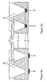
- FIG. 3b Another example of an arrangement according to the invention is shown in Figure 3b.
- the silicon dioxide buffer layer 3 etched through and cavities were created for the recording of samples.
- the waveguide layer is 4 at the bottom of the respective openings 6 with an immobilization layer for the different substances (Biomolecules).
- the breakthroughs 6 can e.g. with a known pipetting device respective samples are introduced and the fluorescence excitation done like this in the description the figure 2 is the case.
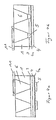
- an intermediate layer 4a and 4b show possible variants for the arrangement of an additional intermediate layer 4a shown that improve the immobilization of the samples should.
- Such an intermediate layer 4a is made of a material transparent to the excitation light and is made with a small thickness (approx. 10 to 50 nm) which ensures that the training of the evanescent field not or only very slightly being affected.
- Suitable materials are e.g. Silicate, quartz, the can be applied using the same process with which the waveguides are also formed. It but can also optically and biologically or chemically suitable polymers used as interlayer material become.
- such an intermediate layer can be used 4a, in a manner not shown, too as a thin liquid film in the openings 6 in the substrate 1 directly between the buffer layer 3 and sample 5 are formed.
- the samples are 5 in the openings 6 of the substrate 1 and between samples 5 and buffer layer 3 Intermediate layer 4a arranged.
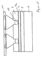
- FIG. 5 uses one structured buffer layer 3a, in which openings 12 are trained. Samples 5 can be used in these Breakthroughs 12 again on the additional intermediate layer 4a can be immobilized. The rest of the corresponding arrangement is here again from the individual elements Substrate 1 (which may be omitted can), waveguide 4 and buffer layer 3 formed, the substrate being unstructured here can.
- the buffer layer provided with the openings 12 3a is made of a material that the waveguide, if at all, only slightly influenced.
- the breakthroughs 12 are designed and dimensioned so that the evanescent field of the waveguide 4 in the area the spaces between the openings 12 the Surface of the buffer layer 3 is not reached and an influence on the fluorescent light excluded is.
- the fluorescence excitation can, as already described, and the fluorescent light emerges from the openings with an appropriate aperture 12 and can be used with the one shown here Micro-optics 11 or a lens array 2 or one structured lens on a detector array, not shown for spatially resolved evaluation of the individual Fluorescence intensities.
Landscapes
- Health & Medical Sciences (AREA)
- Chemical & Material Sciences (AREA)
- Immunology (AREA)
- Physics & Mathematics (AREA)
- Life Sciences & Earth Sciences (AREA)
- Analytical Chemistry (AREA)
- Biochemistry (AREA)
- General Health & Medical Sciences (AREA)
- General Physics & Mathematics (AREA)
- Nuclear Medicine, Radiotherapy & Molecular Imaging (AREA)
- Pathology (AREA)
- Chemical Kinetics & Catalysis (AREA)
- Optics & Photonics (AREA)
- Investigating, Analyzing Materials By Fluorescence Or Luminescence (AREA)
Description
- Figur 1
- ein Ausführungsbeispiel einer erfindungsgemäßen Anordnung mit Fluoreszenzanregung über evaneszentes Feld;
- Figur 2
- ein zweites Ausführungsbeispiel einer erfindungsgemäßen Anordnung mit Fluoreszenzanregung über Mikrolinsenarray;
- Figur 3a
- eine Anordnung nach Figur 1 mit und ohne Linsenarray; Probe auf der umstrukturierten Seite;
- Figur 3b
- eine Anordnung mit bis zur Wellenleiterschicht reichenden Durchbrüchen mit und ohne Linsenarray, und Proben in Durchbrüchen;
- Figur 4a
- eine Anordnung mit zusätzlicher Zwischenschicht und unterhalb von Wellenleiter und Substrat angeordneten Proben;
- Figur 4b
- eine Anordnung mit zusätzlicher Zwischenschicht und oberhalb des/der Wellenleiter angeordneten Proben und
- Figur 5
- eine Anordnung mit einer strukturierten Pufferschicht.
Claims (18)
- Anordnung zur Detektion biochemischer oder chemischer Substanzen mittels Fluoreszenzlichtanregung, bei der
ein plattenförmiges Substrat (1) oder eine Pufferschicht (3) zur Detektion verschiedener Proben (5) lokal definiert strukturiert ist,
dadurch gekennzeichnet, daß die Strukturierung in Form von Durchbrüchen (6) als Fluoreszenznachweiskanal und/oder Fluoreszenzanregungskanal für jeweils eine zu detektierende Probe ausgebildet ist. - Anordnung nach Anspruch 1,
dadurch gekennzeichnet, daß verschiedene selektive Immobilisierungsschichten den verschiedenen Durchbrüchen (6) zugeordnet, aufgebracht sind. - Anordnung nach Anspruch 1 oder 2,
dadurch gekennzeichnet, daß die Durchbrüche (6) pyramiden- oder kegelförmig oder auch senkrecht und zumindest bis zu einer Pufferschicht (3) im Substrat (1) ausgebildet sind. - Anordnung nach einem der Ansprüche 1 bis 3,
dadurch gekennzeichnet, daß detektorseitig ein der Struktur entsprechend ausgebildetes Linsenarray (2) oder eine der Strukturierung angepaßte Linse zur Abbildung des Fluoreszenzlichtes der verschiedenen Proben (5) vor einem Detektorarray angeordnet ist. - Anordnung nach einem der Ansprüche 1 bis 3,
dadurch gekennzeichnet, daß ein entsprechend der Strukturierung des Substrates (1) entsprechend ausgebildetes Detektorarray auf das Substrat (1) aufgesetzt ist. - Anordnung nach einem der Ansprüche 1 bis 5,
dadurch gekennzeichnet, daß die Proben in den Durchbrüchen (6) oder auf der ebenen Seite der Anordnung gegenüber den Durchbrüchen (6) auf der Pufferschicht (3) oder einem Wellenleiter (4), die die Durchbrüche (6) einseitig überdecken, immobilisiert sind. - Anordnung nach einem der Ansprüche 1 bis 6,
dadurch gekennzeichnet, daß das Substrat (1) aus einem das Fluoreszenzlicht absorbierenden Material besteht oder an seiner Oberfläche für Fluoreszenzlicht reflektierend oder absorbierend ausgebildet ist. - Anordnung nach einem der Ansprüche 1 bis 7,
dadurch gekennzeichnet, daß die Wandungen der Durchbrüche (6) Fluoreszenzlicht reflektieren. - Anordnung nach einem der Ansprüche 1 bis 8,
dadurch gekennzeichnet, daß die Anregung der Fluoreszenz über das evaneszente Feld erfolgt. - Anordnung nach Anspruch 1,
dadurch gekennzeichnet, daß auf der einem Linsenarray (2) oder einer Linse abgewandten Seite des Substrates (1) ein Schichtpaket, bestehend aus einer Pufferschicht (3) und mindestens einem Wellenleiter (4) oder einem der Strukturierung angepaßten Wellenleiterarray (4) aufgebracht ist. - Anordnung nach einem der Ansprüche 1 bis 10,
dadurch gekennzeichnet, daß das Substrat (1) aus Silicium, Glas, glasartigem Material oder einem Polymer und die Pufferschicht (3) und der/die Wellenleiter (4) aus einem Silikat, Glas, glasartigem Material oder einem Polymer bestehen. - Anordnung nach einem der Ansprüche 1 bis 8,
dadurch gekennzeichnet, daß das Anregungslicht mindestens einer Lichtquelle (7) über ein zweites Linsenarray (8) oder eine der Strukturierung angepaßte zweite Linse durch ein erstes Linsenarray (2) oder eine erste der Strukturierung angepaßte Linse auf die Proben (5) gerichtet ist. - Anordnung nach einem der Ansprüche 1 bis 8,
dadurch gekennzeichnet, daß zwischen einem ersten und einem zweiten Linsenarray (2, 8) und/oder den Linsen ein halbdurchlässiger Spiegel (9) angeordnet ist. - Anordnung nach einem der Ansprüche 1 bis 13,
dadurch gekennzeichnet, daß auf dem Wellenleiter (4) eine für das Anregungslicht transparente Zwischenschicht (4a), mit einer kleinen Dicke, die die Evaneszentfeldanregung nahezu nicht beeinflußt, auf der die Proben immobilisieren, angeordnet ist. - Verfahren zur Herstellung einer Anordnung nach einem der Ansprüche 1 bis 14,
dadurch gekennzeichnet, daß auf einer Seite eines Substrates (1) eine Pufferschicht (3) aufgebracht und im Substrat (1), ausgehend von der hierzu abgewandten Seite Durchbrechungen (6) zumindest bis zur Pufferschicht (3) ausgebildet werden. - Verfahren zur Herstellung einer Anordnung nach einem der Ansprüche 1 bis 14,
dadurch gekennzeichnet, daß auf einer Seite des Substrates (1) eine Puffer- und eine Wellenleiterschicht (3, 4) aufgebracht, im Substrat (1) ausgehend von der abgewandten Seite Durchbrechungen (6) zumindest bis zur Pufferschicht (3) ausgebildet werden und mit einem Strukturierungsverfahren ein Streifenwellenleiterarray (4) jeweils den Durchbrüchen (6) zugeordnet ausgebildet wird. - Verfahren nach Anspruch 15 oder 16,
dadurch gekennzeichnet, daß auf die Pufferschicht (3) oder die Streifenwellenleiterstruktur (4) verschiedene selektive Immobilisierungsschichten, den Durchbrüchen (6) zugeordnet, aufgebracht werden. - Verfahren nach Anspruch 16 oder 17,
dadurch gekennzeichnet, daß die Durchbrechungen (6) bis zur Streifenwellenleiterstruktur (4) ausgebildet und die verschiedenen Immobilisierungsschichten auf der Streifenwellenleiterstruktur (4) in den Durchbrüchen (6) aufgebracht werden.
Applications Claiming Priority (3)
| Application Number | Priority Date | Filing Date | Title |
|---|---|---|---|
| DE19725050A DE19725050C2 (de) | 1997-06-13 | 1997-06-13 | Anordnung zur Detektion biochemischer oder chemischer Substanzen mittels Fluoreszenzlichtanregung und Verfahren zu deren Herstellung |
| DE19725050 | 1997-06-13 | ||
| PCT/EP1998/003535 WO1998057151A1 (de) | 1997-06-13 | 1998-06-11 | Anordnung zur detektion biochemischer oder chemischer substanzen mittels fluoreszenzlichtanregung und verfahren zu dessen herstellung |
Publications (2)
| Publication Number | Publication Date |
|---|---|
| EP0988526A1 EP0988526A1 (de) | 2000-03-29 |
| EP0988526B1 true EP0988526B1 (de) | 2003-01-02 |
Family
ID=7832407
Family Applications (1)
| Application Number | Title | Priority Date | Filing Date |
|---|---|---|---|
| EP98937475A Expired - Lifetime EP0988526B1 (de) | 1997-06-13 | 1998-06-11 | Anordnung zur detektion biochemischer oder chemischer substanzen mittels fluoreszenzlichtanregung und verfahren zu deren herstellung |
Country Status (4)
| Country | Link |
|---|---|
| US (1) | US6534011B1 (de) |
| EP (1) | EP0988526B1 (de) |
| DE (2) | DE19725050C2 (de) |
| WO (1) | WO1998057151A1 (de) |
Families Citing this family (37)
| Publication number | Priority date | Publication date | Assignee | Title |
|---|---|---|---|---|
| GB9906929D0 (en) * | 1999-03-26 | 1999-05-19 | Univ Glasgow | Assay system |
| DE19919092A1 (de) * | 1999-04-27 | 2000-11-02 | Zeiss Carl Jena Gmbh | Anordnung zur optischen Auswertung eines Gegenstandsarrays |
| US7410793B2 (en) * | 1999-05-17 | 2008-08-12 | Applera Corporation | Optical instrument including excitation source |
| DE19935180C2 (de) * | 1999-07-27 | 2001-08-02 | Fraunhofer Ges Forschung | Solarzellen-Sensoren, Verfahren zu ihrer Herstellung und ihrer Anwendung |
| FR2797054A1 (fr) * | 1999-07-27 | 2001-02-02 | Commissariat Energie Atomique | Dispositif de lecture de puce biologique |
| DE19941270C1 (de) * | 1999-08-31 | 2001-06-28 | Lienhard Pagel | Mikrofluidisches pH-Sensormodul |
| DE10024132B4 (de) * | 2000-01-28 | 2007-03-22 | Leica Microsystems Cms Gmbh | Anordnung zur Detektion von Fluoreszenzlicht mehrerer Probenpunkte |
| DE10017824B4 (de) * | 2000-04-10 | 2004-03-18 | Till I.D. Gmbh | Vorrichtung zur parallelen photometrischen Fluoreszenz- oder Lumineszenzanalyse mehrerer voneinander getrennter Probenbereiche auf einem Objekt |
| EP1311824A4 (de) * | 2000-06-25 | 2010-12-08 | Affymetrix Inc | Optisch aktive substrate |
| FR2813121A1 (fr) * | 2000-08-21 | 2002-02-22 | Claude Weisbuch | Dispositif perfectionne de support d'elements chromophores |
| JP3824135B2 (ja) * | 2001-01-10 | 2006-09-20 | 横河電機株式会社 | バイオチップ読取り装置 |
| US6639201B2 (en) * | 2001-11-07 | 2003-10-28 | Applied Materials, Inc. | Spot grid array imaging system |
| US6946655B2 (en) | 2001-11-07 | 2005-09-20 | Applied Materials, Inc. | Spot grid array electron imaging system |
| AU2002342349A1 (en) | 2001-11-07 | 2003-05-19 | Applied Materials, Inc. | Maskless printer using photoelectric conversion of a light beam array |
| US6707958B2 (en) * | 2001-11-20 | 2004-03-16 | Agilent Technologies, Inc. | Biochemical assay device using frustrated total internal reflection modulator with an imaging optical waveguide |
| DE10160987B4 (de) * | 2001-12-05 | 2005-08-04 | Siemens Ag | Baueinheit zur simultanen, optischen Beleuchtung einer Vielzahl von Proben |
| US7604981B1 (en) * | 2002-03-08 | 2009-10-20 | The Board Of Trustees Of The Leland Stanford Junior University | Excitable target marker detection |
| US9943847B2 (en) | 2002-04-17 | 2018-04-17 | Cytonome/St, Llc | Microfluidic system including a bubble valve for regulating fluid flow through a microchannel |
| US9157860B2 (en) | 2002-05-16 | 2015-10-13 | Applied Biosystems, Llc | Achromatic lens array |
| US6982166B2 (en) * | 2002-05-16 | 2006-01-03 | Applera Corporation | Lens assembly for biological testing |
| JP2005526253A (ja) * | 2002-05-17 | 2005-09-02 | アプレラ コーポレイション | 励起波長による複数の蛍光シグナルを分化するための装置および方法 |
| AU2003239569A1 (en) * | 2002-05-23 | 2003-12-12 | Gene Networks, Inc. | Analyte microdetector and methods for use |
| EP1371966A1 (de) * | 2002-06-14 | 2003-12-17 | Stiftung Für Diagnostische Forschung | Küvette für ein Lesegerät zur Bestimmung von Substanzen mittels der Evaneszenzfeldmethode |
| DE10245432A1 (de) * | 2002-09-27 | 2004-04-08 | Micronas Gmbh | Verfahren und Vorrichtung zum Detektieren mindestens eines Lumineszenz-Stoffs |
| DE10315074A1 (de) | 2003-04-02 | 2004-10-14 | Clondiag Chip Technologies Gmbh | Vorrichtung zur Vervielfältigung und zum Nachweis von Nukleinsäuren |
| US7298478B2 (en) | 2003-08-14 | 2007-11-20 | Cytonome, Inc. | Optical detector for a particle sorting system |
| DE102005052713A1 (de) | 2005-11-04 | 2007-05-16 | Clondiag Chip Tech Gmbh | Vorrichtung und Verfahren zum Nachweis von molekularen Wechselwirkungen |
| DE102004022263A1 (de) | 2004-05-06 | 2005-12-15 | Clondiag Chip Technologies Gmbh | Vorrichtung und Verfahren zum Nachweis von molekularen Wechselwirkungen |
| DE102004056787A1 (de) * | 2004-11-24 | 2006-06-01 | Heinrich-Heine-Universität Düsseldorf | Vorrichtung und Verfahren zur Messung von Fluoreszenz in mehreren Reaktionsräumen |
| AU2005311631B2 (en) | 2004-12-03 | 2012-06-07 | Cytonome/St, Llc | Unitary cartridge for particle processing |
| US9260693B2 (en) | 2004-12-03 | 2016-02-16 | Cytonome/St, Llc | Actuation of parallel microfluidic arrays |
| DE102007031526B4 (de) | 2007-07-06 | 2010-07-08 | Fraunhofer-Gesellschaft zur Förderung der angewandten Forschung e.V. | Verwendung einer Anode in einer Brennstoffzelle zur Oxidation von Ethanol und/oder zumindest eines C3 bis C10-haltigen Alkohols |
| DE102007062250A1 (de) * | 2007-12-21 | 2009-06-25 | Evotec Ag | Vorrichtung zur Untersuchung chemischer und/oder biologischer Proben |
| CN102077080B (zh) * | 2008-06-24 | 2014-06-18 | 皇家飞利浦电子股份有限公司 | 微阵列表征系统和方法 |
| US9989526B2 (en) * | 2013-07-17 | 2018-06-05 | Abionic Sa | Method and device for bioassays |
| JP6439810B2 (ja) | 2017-02-06 | 2018-12-19 | 横河電機株式会社 | バイオチップ、バイオチップユニット、バイオチップ読取装置、及びバイオチップ製造方法 |
| DE102023204533B4 (de) * | 2023-05-15 | 2025-03-27 | Fraunhofer-Gesellschaft zur Förderung der angewandten Forschung eingetragener Verein | Verfahren für die Durchführung von biochemischen Untersuchungen an Proben |
Citations (1)
| Publication number | Priority date | Publication date | Assignee | Title |
|---|---|---|---|---|
| WO1998052024A1 (en) * | 1997-05-13 | 1998-11-19 | Colvin Arthur E Jr | Improved fluorescence sensing device |
Family Cites Families (10)
| Publication number | Priority date | Publication date | Assignee | Title |
|---|---|---|---|---|
| EP0194132A3 (de) * | 1985-03-06 | 1988-08-03 | Murex Corporation | Abbildendes Immunoprobe-Nachweissystem und Verfahren |
| DE4115414C2 (de) * | 1991-05-10 | 1995-07-06 | Meinhard Prof Dr Knoll | Verfahren zur Herstellung von miniaturisierten Chemo- und Biosensorelementen mit ionenselektiver Membran sowie von Trägern für diese Elemente |
| US5156976A (en) * | 1991-06-07 | 1992-10-20 | Ciba Corning Diagnostics Corp. | Evanescent wave sensor shell and apparatus |
| ES2216034T3 (es) | 1992-09-14 | 2004-10-16 | Sri International | Indicadores de conversion creciente destinados a ensayos biologicos y otros utilizando tecnicas de excitacion por laser. |
| US5677196A (en) * | 1993-05-18 | 1997-10-14 | University Of Utah Research Foundation | Apparatus and methods for multi-analyte homogeneous fluoro-immunoassays |
| WO1994027137A2 (en) * | 1993-05-18 | 1994-11-24 | University Of Utah Research Foundation | Apparatus and methods for multianalyte homogeneous fluoroimmunoassays |
| GB9314991D0 (en) * | 1993-07-20 | 1993-09-01 | Sandoz Ltd | Mechanical device |
| AT403745B (de) * | 1996-02-29 | 1998-05-25 | Avl Verbrennungskraft Messtech | Messanordnung mit einem für anregungs- und messstrahlung transparentem trägerelement |
| US5854684A (en) * | 1996-09-26 | 1998-12-29 | Sarnoff Corporation | Massively parallel detection |
| US5827748A (en) * | 1997-01-24 | 1998-10-27 | The United States Of America As Represented By The Secretary Of The Navy | Chemical sensor using two-dimensional lens array |
-
1997
- 1997-06-13 DE DE19725050A patent/DE19725050C2/de not_active Expired - Fee Related
-
1998
- 1998-06-11 WO PCT/EP1998/003535 patent/WO1998057151A1/de not_active Ceased
- 1998-06-11 DE DE59806826T patent/DE59806826D1/de not_active Expired - Lifetime
- 1998-06-11 EP EP98937475A patent/EP0988526B1/de not_active Expired - Lifetime
- 1998-06-11 US US09/445,819 patent/US6534011B1/en not_active Expired - Fee Related
Patent Citations (1)
| Publication number | Priority date | Publication date | Assignee | Title |
|---|---|---|---|---|
| WO1998052024A1 (en) * | 1997-05-13 | 1998-11-19 | Colvin Arthur E Jr | Improved fluorescence sensing device |
Also Published As
| Publication number | Publication date |
|---|---|
| WO1998057151A1 (de) | 1998-12-17 |
| DE19725050A1 (de) | 1998-12-17 |
| DE59806826D1 (de) | 2003-02-06 |
| US6534011B1 (en) | 2003-03-18 |
| EP0988526A1 (de) | 2000-03-29 |
| DE19725050C2 (de) | 1999-06-24 |
Similar Documents
| Publication | Publication Date | Title |
|---|---|---|
| DE19725050C2 (de) | Anordnung zur Detektion biochemischer oder chemischer Substanzen mittels Fluoreszenzlichtanregung und Verfahren zu deren Herstellung | |
| DE19923820C2 (de) | SPR-Sensor zur gleichzeitigen Erfassung einer Vielzahl von in fluider Form vorliegenden Proben | |
| EP1274986B1 (de) | Vorrichtung und verfahren zur multianalytbestimmung | |
| DE69724943T2 (de) | Mikrohergestellter chemischer sensor auf diffusionsbasis | |
| DE102007033124B4 (de) | Vorrichtung zur optischen Detektion von Substanzen in einem flüssigen oder gasförmigen Medium | |
| DE69637315T2 (de) | Verfahren zur parallelen bestimmung mehrerer analyten mittels evaneszent angeregter lumineszenz | |
| DE19628002C1 (de) | Vorrichtung und Verfahren zur Durchführung von Fluoreszenzimmunotests | |
| EP1257809B1 (de) | Spr-sensor und spr-sensoranordnung | |
| EP1556695B1 (de) | Analytische plattform und nachweisverfahren mit gegebenenfalls nach fraktionierung in einer probe nachzuweisenden analyten als immobilisierten spezifischen bindungspartnern | |
| DE10012793C2 (de) | Sensorelement zur optischen Detektion von chemischen oder biochemischen Analyten | |
| DE102005062174C5 (de) | Meßchip | |
| EP1443320A2 (de) | Sensorchip zur Charakterisierung einer chemischen und/oder biochemischen Substanz | |
| WO1999040415A1 (de) | Verfahren und vorrichtung zur lumineszenzmessung | |
| EP1190236A1 (de) | Sensorplatform und verfahren zur multianalytbestimmung | |
| AT513859B1 (de) | Mikro-Fluoreszenzdetektionsvorrichtung sowie Verfahren zur Detektion | |
| EP1347284B1 (de) | Probenträger mit integrierter Optik | |
| EP1017994A1 (de) | Diffusionsbasierter chemischer sensor für mehrere analyte | |
| DE19545130C2 (de) | Verfahren und Vorrichtungen für ein modulares Mikrosystem für hochgenaue chemische Schnell-Analysen | |
| DE60114656T2 (de) | Chip-element für mikrochemische systeme und ein das chip-element verwendendes mikrochemisches system | |
| DE60020702T2 (de) | Abbildende assay-analyse für mikroproben | |
| DE19647644C2 (de) | Mikromechanische Transmissionsmeßzelle | |
| EP3968008B1 (de) | Optischer sensor, system und verfahren zum nachweis pathogener keime | |
| DE10324973B4 (de) | Anordnung und Verfahren zur optischen Detektion von in Proben enthaltenen chemischen, biochemischen Molekülen und/oder Partikeln | |
| WO2001052975A1 (de) | Kapillarkraftmischer | |
| EP2718691B1 (de) | Verfahren und vorrichtung zum bestimmen der konzentration eines in einer flüssigen probe enthaltenen analyten |
Legal Events
| Date | Code | Title | Description |
|---|---|---|---|
| PUAI | Public reference made under article 153(3) epc to a published international application that has entered the european phase |
Free format text: ORIGINAL CODE: 0009012 |
|
| 17P | Request for examination filed |
Effective date: 19991109 |
|
| AK | Designated contracting states |
Kind code of ref document: A1 Designated state(s): CH DE FR GB IT LI |
|
| RIN1 | Information on inventor provided before grant (corrected) |
Inventor name: DANZ, NORBERT Inventor name: WALDHAEUSL, RALF Inventor name: KOEHLER, MICHAEL Inventor name: EISMANN, FRANK Inventor name: BRAEUER, ANDREAS Inventor name: KARTHE, WOLFGANG, PROF. DR. |
|
| 17Q | First examination report despatched |
Effective date: 20010510 |
|
| GRAG | Despatch of communication of intention to grant |
Free format text: ORIGINAL CODE: EPIDOS AGRA |
|
| GRAG | Despatch of communication of intention to grant |
Free format text: ORIGINAL CODE: EPIDOS AGRA |
|
| GRAH | Despatch of communication of intention to grant a patent |
Free format text: ORIGINAL CODE: EPIDOS IGRA |
|
| GRAH | Despatch of communication of intention to grant a patent |
Free format text: ORIGINAL CODE: EPIDOS IGRA |
|
| GRAA | (expected) grant |
Free format text: ORIGINAL CODE: 0009210 |
|
| AK | Designated contracting states |
Kind code of ref document: B1 Designated state(s): CH DE FR GB IT LI |
|
| PG25 | Lapsed in a contracting state [announced via postgrant information from national office to epo] |
Ref country code: IT Free format text: LAPSE BECAUSE OF FAILURE TO SUBMIT A TRANSLATION OF THE DESCRIPTION OR TO PAY THE FEE WITHIN THE PRE;WARNING: LAPSES OF ITALIAN PATENTS WITH EFFECTIVE DATE BEFORE 2007 MAY HAVE OCCURRED AT ANY TIME BEFORE 2007. THE CORRECT EFFECTIVE DATE MAY BE DIFFERENT FROM THE ONE RECORDED.SCRIBED TIME-LIMIT Effective date: 20030102 Ref country code: GB Free format text: LAPSE BECAUSE OF FAILURE TO SUBMIT A TRANSLATION OF THE DESCRIPTION OR TO PAY THE FEE WITHIN THE PRESCRIBED TIME-LIMIT Effective date: 20030102 Ref country code: FR Free format text: LAPSE BECAUSE OF FAILURE TO SUBMIT A TRANSLATION OF THE DESCRIPTION OR TO PAY THE FEE WITHIN THE PRESCRIBED TIME-LIMIT Effective date: 20030102 |
|
| RAP2 | Party data changed (patent owner data changed or rights of a patent transferred) |
Owner name: FRAUNHOFER-GESELLSCHAFT ZUR FOERDERUNG DER ANGEWAN |
|
| REG | Reference to a national code |
Ref country code: GB Ref legal event code: FG4D Free format text: 20030102:NOT ENGLISH |
|
| REG | Reference to a national code |
Ref country code: CH Ref legal event code: EP |
|
| REF | Corresponds to: |
Ref document number: 59806826 Country of ref document: DE Date of ref document: 20030206 Kind code of ref document: P |
|
| REG | Reference to a national code |
Ref country code: CH Ref legal event code: NV Representative=s name: TROESCH SCHEIDEGGER WERNER AG |
|
| GBV | Gb: ep patent (uk) treated as always having been void in accordance with gb section 77(7)/1977 [no translation filed] |
Effective date: 20030102 |
|
| PLBE | No opposition filed within time limit |
Free format text: ORIGINAL CODE: 0009261 |
|
| STAA | Information on the status of an ep patent application or granted ep patent |
Free format text: STATUS: NO OPPOSITION FILED WITHIN TIME LIMIT |
|
| RAP2 | Party data changed (patent owner data changed or rights of a patent transferred) |
Owner name: FRAUNHOFER-GESELLSCHAFT ZUR FOERDERUNG DERANGEWAND |
|
| EN | Fr: translation not filed | ||
| 26N | No opposition filed |
Effective date: 20031003 |
|
| REG | Reference to a national code |
Ref country code: CH Ref legal event code: PFA Owner name: FRAUNHOFER-GESELLSCHAFT ZUR FOERDERUNG DER ANGEWA Free format text: FRAUNHOFER-GESELLSCHAFT ZUR FOERDERUNG DER ANGEWANDTEN FORSCHUNG E.V.#LEONRODSTRASSE 54#80636 MUENCHEN (DE) -TRANSFER TO- FRAUNHOFER-GESELLSCHAFT ZUR FOERDERUNG DER ANGEWANDTEN FORSCHUNG E.V.#HANSASTRASSE 27 C#80686 MUENCHEN (DE) |
|
| PGFP | Annual fee paid to national office [announced via postgrant information from national office to epo] |
Ref country code: CH Payment date: 20100624 Year of fee payment: 13 |
|
| PGFP | Annual fee paid to national office [announced via postgrant information from national office to epo] |
Ref country code: DE Payment date: 20100825 Year of fee payment: 13 |
|
| REG | Reference to a national code |
Ref country code: CH Ref legal event code: PL |
|
| REG | Reference to a national code |
Ref country code: DE Ref legal event code: R119 Ref document number: 59806826 Country of ref document: DE Effective date: 20120103 |
|
| PG25 | Lapsed in a contracting state [announced via postgrant information from national office to epo] |
Ref country code: DE Free format text: LAPSE BECAUSE OF NON-PAYMENT OF DUE FEES Effective date: 20120103 Ref country code: CH Free format text: LAPSE BECAUSE OF NON-PAYMENT OF DUE FEES Effective date: 20110630 Ref country code: LI Free format text: LAPSE BECAUSE OF NON-PAYMENT OF DUE FEES Effective date: 20110630 |