EP0981217B1 - Modulating method, modulating device, demodulating method, and demodulating device - Google Patents
Modulating method, modulating device, demodulating method, and demodulating device Download PDFInfo
- Publication number
- EP0981217B1 EP0981217B1 EP99902898A EP99902898A EP0981217B1 EP 0981217 B1 EP0981217 B1 EP 0981217B1 EP 99902898 A EP99902898 A EP 99902898A EP 99902898 A EP99902898 A EP 99902898A EP 0981217 B1 EP0981217 B1 EP 0981217B1
- Authority
- EP
- European Patent Office
- Prior art keywords
- data
- fourier transform
- supplied
- processing
- interleaved
- Prior art date
- Legal status (The legal status is an assumption and is not a legal conclusion. Google has not performed a legal analysis and makes no representation as to the accuracy of the status listed.)
- Expired - Lifetime
Links
Images

Classifications
-
- H—ELECTRICITY
- H04—ELECTRIC COMMUNICATION TECHNIQUE
- H04L—TRANSMISSION OF DIGITAL INFORMATION, e.g. TELEGRAPHIC COMMUNICATION
- H04L27/00—Modulated-carrier systems
- H04L27/26—Systems using multi-frequency codes
- H04L27/2601—Multicarrier modulation systems
- H04L27/2647—Arrangements specific to the receiver only
Definitions
- the present invention relates to a modulating method for generating a signal modulated by orthogonal frequency division multiplexing (to be referred to as 'OFDM' hereinafter), a modulator utilizing the modulation method, a demodulating method for demodulating the OFDM-modulated signal and a demodulator utilizing the demodulation method.
- the present invention relates to, in particular, a technique suited for processing an interleaved OFDM modulation signal.
- OFDM modulation has been put to practical use as one of modulation systems in case of radio-transmitting relatively mass storage digital data.
- a picture signal digital picture data
- a picture signal source 1 consisting of a tuner receiving television broadcasting, a reproducing apparatus for reproducing a picture program recorded in a recording medium and the like
- the picture signal is modulated to an OFDM modulated signal at a radio transmitter 2 and the modulated signal is radio-transmitted from an antenna 3 in a predetermined frequency band.
- the radio-transmitted signal is received by a radio receiver 5 connected to an antenna 4.
- the received OFDM wave in the frequency band is demodulated and a picture signal is thereby obtained.
- the received picture signal is supplied to a video recording and reproducing apparatus 6, in which the signal is recorded in a predetermined recording medium such as a video tape, or supplied to an image receiving machine 7 and subjected to image receiving process. In this case, it is possible to reproduce the picture signal recorded in the video recording and reproducing apparatus 6 and to supply the resultant reproduced signal to the image receiving machine 7 to thereby allow an image to be received by the image receiving machine 7.
- a transmission signal (digital data) obtained at an input terminal 2a is supplied to a serial/ parallel converter 2b and converted to parallel data for each predetermined unit.
- the parallel data converted at the serial/ parallel converter 2b is supplied to an interleave memory 2c in which interleave processing for changing write and read orders for writing and reading data to/from the memory 2c and changing data array.
- the interleaved parallel data is supplied to an inverse Fourier transform circuit (or IFFT circuit) 2d, in which time axis data is orthogonally transformed to frequency axis data by arithmetic operation by means of inverse fast Fourier transform.
- the orthogonally transformed parallel data is supplied to a parallel/serial converter 2e and converted to serial data, which serial data is supplied to an output terminal 2f.
- the data obtained at the output terminal 2f is supplied to a transmission processing system to convert the frequency to fall within the range of a predetermined transmission frequency band, thereafter radio-transmitting the data.
- EP-A-0,673,131 discloses a modulator for performing orthogonal frequency division multiplexing modulation of input data.
- the modulator includes an interleaver which generates interleaved data from the input data and an inverse Fourier transform circuit supplied with the interleaved data and arranged to perform an inverse Fourier transform thereof to generate orthogonal frequency division multiplexed modulated data.
- a signal in a predetermined frequency band is received and a signal frequency-converted to an intermediate frequency signal is obtained at the input terminal 5a.
- the data obtained at the input terminal 5a is supplied to a serial/parallel converter 5b and converted to parallel data for each predetermined unit.
- the converted output is supplied to a Fourier transform circuit (FFT circuit) 5c, in which orthogonal transform processing for transforming frequency axis data to time axis data by arithmetic operation by means of fast Fourier transform.
- FFT circuit Fourier transform circuit
- the orthogonally transformed parallel data is supplied to a de-interleave memory 5d, in which de-interleave processing for changing write and read orders for writing and reading data to/from the memory 5d, changing data array back to an original data array is conducted.
- the de-interleaved parallel data is supplied to the parallel/serial converter 5e and converted to serial data, which serial data is supplied to the output terminal 5f.
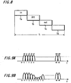
- the demodulation processing for demodulating the OFDM modulation signal conducted with the constitution shown in FIG. 25 is executed at timing shown in FIG. 8 . That is to say, there are, first, a data input time Ta at which data is inputted to the Fourier transform circuit 5c, next a Fourier transform processing time Tb at which Fast Fourier transform is conducted at the Fourier transform circuit 5c and then a data output time Tc at which the Fourier-transformed data is outputted.
- the data outputted at the output time Tc is simultaneously written in the de-interleave memory 5d and the data written in the memory 5d is read at a read-out time Td.
- transform processing for generating an OFDM modulation signal with the constitution of FIG. 6 is basically opposite to the demodulation processing and requires the same time as that for the demodulation processing.
- FIG. 11 shows an example of the latter case. Processing steps shown therein are the same until data obtained at an input terminal 5a is supplied to a serial/parallel converter 5b and converted to parallel data for each predetermined unit, and the conversion output is supplied to a Fourier transform circuit 5c, in which orthogonal transform for transforming frequency axis data to time axis data is conducted by arithmetic operation by means of Fast Fourier transform.
- the orthogonally transformed parallel data is subjected to processing for changing a data array by wiring change processing 5d corresponding to the interleave pattern of the data.
- the parallel data which data array has been thus changed is supplied to a parallel/serial converter 5e and converted to serial data.
- the serial data is then supplied to an output terminal 5f.
- the demodulation processing for demodulating an OFDM modulation signal conducted with the constitution shown in FIG. 29 is executed at timing shown in FIG. 12 . That is to say, there are, first, a data input time Te at which data is inputted to the Fourier transform circuit 5c, next a Fourier transform processing time Tf at which fast Fourier transform is conducted at the Fourier transform circuit 5c, and then an output time Tg at which the data thus Fourier-transformed is outputted.
- the data is outputted from the Fourier transform circuit 5c and supplied to the parallel/serial converter 5e and, at the same time, de-interleaved by wiring change processing 5d.
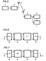
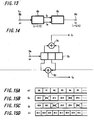
- FIG. 13 shows an example of a conventional constitution with which this puncture processing is conducted.
- Transmission data a i obtained at an input terminal 8a is convolutionally coded by a convolutional coder 8b and two sets of data G 1 and G 2 are generated.
- the two data sets G 1 and G 2 are supplied to a thinning-out processing circuit 8c and thinned out, and coded data b i which has been subjected to puncture processing is thereby obtained.
- transmission data a i obtained at the input terminal 9a is supplied to a shift register 9b.
- the shift register 9b consists of three stages, in which data stored in the first stage and that in the third stage are supplied to and added together by an adder 9c and data G 1 is thereby obtained and in which data stored in the first stage and that in the second stage are supplied to and added together by an adder 9d and data G 2 is thereby obtained.
- FIG. 15 The thinning-out processing state of the two data sets of G 1 and G 2 thus convolutionally coded is shown in FIG. 15 .
- a data sequence of a 0 , a 1 , a 2 ... shown in, for example, FIG. 15A forms input data ai
- two data sets G 1 and G 2 which have been convolutionally coded become data g 10 , g 11 , g 12 , ... and data g 20 , g 21 , g 22 , ... as shown in FIGS. 15B and 15C , respectively.
- a thinning-out processing circuit 8c using, for example, data g 10 , g 11 , g 12 , g 20 , g 21 and g 22 , the data are outputted in the order of g 10 , g 20 , g 21 and g 12 as shown in FIG. 15D .
- data g 11 and g 22 are thinned out.
- modulation processing for modulating an OFDM modulation signal if interleave processing is conducted using a memory as shown in FIG. 5 , a modulation processing constitution is disadvantageously complicated because of the need of the memory. Also, the modulation processing time is disadvantageously longer than that for a case where data which is not interleaved is processed by the time required for reading data from the interleave memory.
- the constitution for puncture processing is disadvantageously complicated. That is, as can be seen from FIG. 15 showing a puncture processing state, the clock rate of input data ( FIG. 15A ) is not an integral multiple of that of puncture-processed output data ( FIG. 15B ). A clock of two-thirds of a data clock fj is required for thinning-out processing and the generation of such clocks tends to make constitution complex. Besides, it also requires processing for re-timing the thinned-out data, which makes a relevant circuit larger in size and it requires high power consumption.
- a modulation method of performing orthogonal frequency division multiplexing modulation of input data comprising:
- the method further comprises differentially encoding each of the first set and the second set of interleaved data in parallel, the differentially encoded first set and the differentially encoded second set of interleaved data being supplied in parallel to the inverse Fourier transform circuit.
- the step of generating the first set and the second set of interleaved data comprises supplying the input data to first and second shift registers and reading data set to the first and second shift registers in parallel, the data set to each of the first and second shift register being read in a predetermined order corresponding to an interleave pattern to generate, respectively, the first set and the second set of interleaved data.
- a modulator for performing orthogonal frequency division multiplexing modulation of input data comprising:
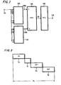
- FIG. 1 shows the constitution of the modulator part in this embodiment.
- Transmission data a i such as a base band signal is supplied to an input terminal 141.
- the transmission data a i obtained at the input terminal 141 is interleaved and OFDM modulated.
- the transmission data a i obtained at the input terminal 141 is supplied to two shift registers 142 and 143 and stored therein.
- the data set to the shift registers 142 and 143 are read in a predetermined order corresponding to an interleave pattern and simultaneously supplied to an inverse Fourier transform circuit 144. That is to say, the inverse Fourier transform circuit 144 in this embodiment is provided with two input terminals 144a and 144b.
- the inverse Fourier transform circuit 144 is a circuit conducting orthogonal transform processing for transforming and then modulating time axis data to frequency axis data by arithmetic operation by means of inverse Fourier transform.
- An inverse Fourier transform circuit which conducts N-point (64-point in this case) transform processing is employed herein and the circuit outputs the transformed data as N-bit (64-bit) parallel data.
- the shift registers 142 and 143 are designed such that 32 points of data can be set thereto, respectively.
- the parallel data outputted from the inverse Fourier transform circuit 144 is supplied to a parallel/serial converter 145 and converted to serial data.
- the serial data is supplied to an output terminal 146 as OFDM-modulated data y n .
- the OFDM-modulated data y n is supplied to a high frequency circuit (not shown) in which the data y n is subjected to transmission processing.
- FIG. 2 is a timing view showing a modulation processing state in the circuit in this embodiment, which processing state will be described hereinafter.
- an input time Tm at which 64 points of data obtained at the input terminal 141 are inputted to the two shift registers 142 and 143.
- an interleave processing time Tn at which the data set to the two shift registers 142 and 143 at the input time Tm are simultaneously inputted to the inverse Fourier transform circuit 144 in the order set by the shift registers 142 and 143.
- the interleave processing time Tn may be half the input time Tm. In case of 64 points of data, for example, the interleave processing time Tn may be a 32-clock time.
- a time T 4 shown in FIG. 2 includes a shorter time required for interleave processing and processing time is shorter than that at the modulation processing circuit shown as a conventional case in FIG. 6 .
- time or processing time corresponding to 32-clock time for input data can be shortened.
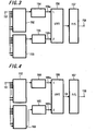
- FIG. 3 shows the constitution of the modulator part in this embodiment.
- Transmission data a i such as a base band signal is supplied to an input terminal 151.
- the transmission data ai obtained at the input terminal 151 is interleaved and OFDM modulated.
- the transmission data ai obtained at the input terminal 151 is supplied to two shift registers 152 and 153 and stored therein.
- the data set to the respective shift registers 152 and 153 are read in a predetermined order corresponding to an interleave pattern.
- the data outputted from the shift registers 152 and 153 are supplied to differential coding circuit 154 and 155, respectively and differentially coded.
- the data differentially coded at the respective circuits are simultaneously supplied to two input terminals 156a and 156b of an inverse Fourier transform circuit 156.
- the inverse Fourier transform circuit 156 is a circuit conducting orthogonal transform processing for transforming and then modulating time axis data to frequency axis data by arithmetic operation by means of inverse Fourier transform.
- an inverse Fourier transform circuit conducting N-point (64-point in this case) transform processing is employed and the circuit outputs the transformed data as N-bit (64-bit) parallel data.
- the shift registers 152 and 153 are designed such that 32 points of data can be set thereto, respectively.
- the parallel data outputted from the inverse Fourier transform circuit 156 is supplied to a parallel/serial converter 157 and converted to serial data.
- the serial data is supplied to an output terminal 158 as OFDM-modulated data y n .
- the OFDM-modulated data y n obtained at the output terminal 158 is supplied to a high frequency circuit (not shown) in which the data y n is subjected to transmission processing.
- this embodiment With the constitution of this embodiment in which the above-described processing is conducted, as in the case of the first embodiment, it is possible to halve time required for interleave processing compared to the conventionally required time, by which degree time required for processing for generating an interleaved OFDM modulation signal can be shortened.
- a differential coding processing is conducted at the input parts of the inverse Fourier transform circuit. This makes it possible to OFDM-modulate the differentially coded data and to conduct efficient OFDM modulation based on the differentially coded data.
- the present invention is applied to a modulator part in a transmitter radio-transmitting an OFDM modulation signal.
- An OFDM modulation signal to be transmitted is interleaved.
- FIG. 4 shows the constitution of the modulator part in this embodiment.
- Transmission data ai such as a base band signal is supplied to an input terminal 161.
- the transmission data ai obtained at the input terminal 161 is interleaved and OFDM modulated.
- the transmission data ai obtained at the input terminal 161 is supplied to two shift registers 162 and 163 and stored therein.
- the data set to the shift registers 162 and 163 are read in a predetermined order corresponding to an interleave pattern.
- the read-out order of the shift register 162 is set opposite to that of the shift register 163.
- the shift register 162 is read the set data from the beginning, whereas the shift register 163 reads the set data from the end.
- the inverse Fourier transform circuit 166 is a circuit conducting orthogonal transform processing for transforming and then modulating time axis data to frequency axis data by arithmetic operation by means of inverse Fourier transform.
- an inverse Fourier transform circuit conducting N-point (64-point in this case) transform processing is employed and the circuit outputs the transformed data as N-bit (64-bit) parallel data.
- the shift registers 162 and 163 are designed such that 32 points of data can be set thereto, respectively.
- the parallel data outputted from the inverse Fourier transform circuit 166 is supplied to a parallel/serial converter 167 and converted to serial data.
- the serial data is supplied to an output terminal 168 as OFDM-modulated data y n .
- the OFDM-modulated data y n obtained at the output terminal 168 is supplied to a high frequency circuit (not shown) and subjected to transmission processing.
- the OFDM-modulated signal generated with the constitution of the sixth embodiment is a signal shown in, for example, FIG. 3B
- the OFDM-modulated signal generated with the constitution of this ( seventh) embodiment has the data array of points 39 to 63 (-25 to -1) of the signal shown in FIG. 3B opposite to that in the sixth embodiment.
Landscapes
- Engineering & Computer Science (AREA)
- Computer Networks & Wireless Communication (AREA)
- Signal Processing (AREA)
- Error Detection And Correction (AREA)
- Detection And Prevention Of Errors In Transmission (AREA)
- Transmission Systems Not Characterized By The Medium Used For Transmission (AREA)
- Digital Transmission Methods That Use Modulated Carrier Waves (AREA)
Applications Claiming Priority (5)
| Application Number | Priority Date | Filing Date | Title |
|---|---|---|---|
| JP3162098 | 1998-02-13 | ||
| JP3162098 | 1998-02-13 | ||
| JP9963198 | 1998-04-10 | ||
| JP10099631A JPH11298436A (ja) | 1998-02-13 | 1998-04-10 | 変調方法、変調装置、復調方法及び復調装置 |
| PCT/JP1999/000624 WO1999041865A1 (en) | 1998-02-13 | 1999-02-12 | Modulating method, modulating device, demodulating method, and demodulating device |
Publications (3)
| Publication Number | Publication Date |
|---|---|
| EP0981217A1 EP0981217A1 (en) | 2000-02-23 |
| EP0981217A4 EP0981217A4 (en) | 2005-11-23 |
| EP0981217B1 true EP0981217B1 (en) | 2012-09-12 |
Family
ID=26370119
Family Applications (1)
| Application Number | Title | Priority Date | Filing Date |
|---|---|---|---|
| EP99902898A Expired - Lifetime EP0981217B1 (en) | 1998-02-13 | 1999-02-12 | Modulating method, modulating device, demodulating method, and demodulating device |
Country Status (5)
| Country | Link |
|---|---|
| US (1) | US6826239B1 (enExample) |
| EP (1) | EP0981217B1 (enExample) |
| JP (1) | JPH11298436A (enExample) |
| CN (1) | CN1263659B (enExample) |
| WO (1) | WO1999041865A1 (enExample) |
Families Citing this family (4)
| Publication number | Priority date | Publication date | Assignee | Title |
|---|---|---|---|---|
| US7158474B1 (en) | 2001-02-21 | 2007-01-02 | At&T Corp. | Interference suppressing OFDM system for wireless communications |
| US20040268207A1 (en) * | 2003-05-21 | 2004-12-30 | Engim, Inc. | Systems and methods for implementing a rate converting, low-latency, low-power block interleaver |
| JP3877215B2 (ja) * | 2003-10-10 | 2007-02-07 | 株式会社インテリジェント・コスモス研究機構 | 送信装置、通信システムおよび通信方法 |
| WO2011013251A1 (ja) | 2009-07-31 | 2011-02-03 | 株式会社 東芝 | 信号受信装置および通信システム |
Family Cites Families (11)
| Publication number | Priority date | Publication date | Assignee | Title |
|---|---|---|---|---|
| JPS5815353A (ja) * | 1981-07-21 | 1983-01-28 | Toshiba Corp | デ−タ復調回路 |
| US4615040A (en) * | 1984-06-14 | 1986-09-30 | Coenco Ltd. | High speed data communications system |
| GB9218874D0 (en) * | 1992-09-07 | 1992-10-21 | British Broadcasting Corp | Improvements relating to the transmission of frequency division multiplex signals |
| JP3579076B2 (ja) | 1994-03-15 | 2004-10-20 | 三洋電機株式会社 | 量子効果デバイス |
| JP3139909B2 (ja) * | 1994-03-15 | 2001-03-05 | 株式会社東芝 | 階層的直交周波数多重伝送方式および送受信装置 |
| KR100247373B1 (ko) * | 1994-08-31 | 2000-03-15 | 이데이 노부유끼 | 신호 송신 장치, 신호 수신 장치, 및 신호 송수신방법 |
| JP3304632B2 (ja) * | 1994-09-21 | 2002-07-22 | ソニー株式会社 | インターリーブ方法およびインターリーブ回路 |
| EP0719001A1 (en) * | 1994-12-22 | 1996-06-26 | ALCATEL BELL Naamloze Vennootschap | DMT modulator |
| US5949796A (en) * | 1996-06-19 | 1999-09-07 | Kumar; Derek D. | In-band on-channel digital broadcasting method and system |
| EP0855657B1 (en) * | 1997-01-22 | 2007-03-14 | Matsushita Electric Industrial Co., Ltd. | Fast fourier transforming apparatus and method |
| JPH11298437A (ja) * | 1998-04-10 | 1999-10-29 | Sony Corp | 復調方法及び復調装置 |
-
1998
- 1998-04-10 JP JP10099631A patent/JPH11298436A/ja active Pending
-
1999
- 1999-02-12 EP EP99902898A patent/EP0981217B1/en not_active Expired - Lifetime
- 1999-02-12 US US09/402,758 patent/US6826239B1/en not_active Expired - Fee Related
- 1999-02-12 WO PCT/JP1999/000624 patent/WO1999041865A1/ja not_active Ceased
- 1999-02-12 CN CN99800505.3A patent/CN1263659B/zh not_active Expired - Fee Related
Non-Patent Citations (1)
| Title |
|---|
| WOLD E.H.; DESPAIN A.M.: "PIPELINE AND PARALLEL-PIPELINE FFT PROCESSORS FOR VLSI IMPLEMENTATIONS", IEEE TRANSACTIONS ON COMPUTERS, vol. C33, 1 May 1984 (1984-05-01), LOS ALAMITOS, CA, US, pages 414 - 426 * |
Also Published As
| Publication number | Publication date |
|---|---|
| EP0981217A1 (en) | 2000-02-23 |
| CN1263659A (zh) | 2000-08-16 |
| EP0981217A4 (en) | 2005-11-23 |
| CN1263659B (zh) | 2010-09-29 |
| US6826239B1 (en) | 2004-11-30 |
| WO1999041865A1 (en) | 1999-08-19 |
| JPH11298436A (ja) | 1999-10-29 |
Similar Documents
| Publication | Publication Date | Title |
|---|---|---|
| JP4351762B2 (ja) | 無線情報伝送装置及び無線情報伝送方法 | |
| US9100251B2 (en) | Data processing apparatus and method for interleaving and deinterleaving data | |
| CA2344117C (en) | Method and system for tiered digital television terrestrial broadcasting services using multi-bit-stream frequency interleaved ofdm | |
| EP0651926A1 (en) | Transmitting and receiving apparatus and method including punctured convolutional encoding and decoding | |
| JP2008295057A (ja) | 直交周波数分割多重通信方式によるデジタル信号の送信 | |
| US6169768B1 (en) | Receiving apparatus and method | |
| EP0827300B1 (en) | Data receiver and data receiving method for punctured, convolutionally-encoded data | |
| JP3521016B2 (ja) | 直交周波数分割多重信号の受信方法および受信装置 | |
| EP0981217B1 (en) | Modulating method, modulating device, demodulating method, and demodulating device | |
| JP3900670B2 (ja) | 通信装置 | |
| US6067330A (en) | Demodulation method and demodulation apparatus | |
| US7577160B2 (en) | MB-OFDM transmitter and receiver and signal processing method thereof | |
| JP5149130B2 (ja) | Mimo送信装置、受信装置およびシステム | |
| JP3565537B2 (ja) | 直交周波数分割多重変調信号の伝送方式 | |
| JP2987367B1 (ja) | データ伝送方式およびその送受信装置 | |
| JP3575985B2 (ja) | 周波数分割多重信号送信装置におけるデータ処理方法 | |
| JP2000341245A (ja) | 通信システム、受信機及びデジタルデータ復調器 | |
| JPH0225306B2 (enExample) | ||
| JPH09116462A (ja) | スペクトル拡散方式通信装置 | |
| KR0142312B1 (ko) | 디지탈전송신호의 자동동기검출시스템 | |
| JPH098703A (ja) | 周波数ホッピング通信における送信装置及び受信装置並びに周波数ホッピング通信における誤り訂正方法 | |
| JP2001136145A (ja) | 周波数分割多重信号受信装置及び周波数分割多重信号受信方法 | |
| KR20000010355A (ko) | 오에프디엠 시스템의 티피에스 동기 획득 방법및 장치 | |
| JP2001211087A (ja) | 無線通信システム及びその方法 | |
| JP2003249909A (ja) | 直交周波数分割多重信号の空間ダイバーシティ受信装置 |
Legal Events
| Date | Code | Title | Description |
|---|---|---|---|
| PUAI | Public reference made under article 153(3) epc to a published international application that has entered the european phase |
Free format text: ORIGINAL CODE: 0009012 |
|
| 17P | Request for examination filed |
Effective date: 19991112 |
|
| AK | Designated contracting states |
Kind code of ref document: A1 Designated state(s): DE FR GB |
|
| A4 | Supplementary search report drawn up and despatched |
Effective date: 20051007 |
|
| RIC1 | Information provided on ipc code assigned before grant |
Ipc: 7H 04L 27/26 B Ipc: 7H 03M 13/00 B Ipc: 7H 04J 11/00 A |
|
| 17Q | First examination report despatched |
Effective date: 20061113 |
|
| GRAP | Despatch of communication of intention to grant a patent |
Free format text: ORIGINAL CODE: EPIDOSNIGR1 |
|
| RTI1 | Title (correction) |
Free format text: MODULATING METHOD, MODULATING DEVICE, DEMODULATING METHOD, AND DEMODULATING DEVICE |
|
| GRAS | Grant fee paid |
Free format text: ORIGINAL CODE: EPIDOSNIGR3 |
|
| GRAA | (expected) grant |
Free format text: ORIGINAL CODE: 0009210 |
|
| AK | Designated contracting states |
Kind code of ref document: B1 Designated state(s): DE FR GB |
|
| REG | Reference to a national code |
Ref country code: GB Ref legal event code: FG4D |
|
| REG | Reference to a national code |
Ref country code: DE Ref legal event code: R096 Ref document number: 69944397 Country of ref document: DE Effective date: 20121108 |
|
| PGFP | Annual fee paid to national office [announced via postgrant information from national office to epo] |
Ref country code: DE Payment date: 20130219 Year of fee payment: 15 Ref country code: FR Payment date: 20130301 Year of fee payment: 15 Ref country code: GB Payment date: 20130218 Year of fee payment: 15 |
|
| PLBE | No opposition filed within time limit |
Free format text: ORIGINAL CODE: 0009261 |
|
| STAA | Information on the status of an ep patent application or granted ep patent |
Free format text: STATUS: NO OPPOSITION FILED WITHIN TIME LIMIT |
|
| 26N | No opposition filed |
Effective date: 20130613 |
|
| REG | Reference to a national code |
Ref country code: DE Ref legal event code: R097 Ref document number: 69944397 Country of ref document: DE Effective date: 20130613 |
|
| REG | Reference to a national code |
Ref country code: DE Ref legal event code: R119 Ref document number: 69944397 Country of ref document: DE |
|
| GBPC | Gb: european patent ceased through non-payment of renewal fee |
Effective date: 20140212 |
|
| REG | Reference to a national code |
Ref country code: FR Ref legal event code: ST Effective date: 20141031 |
|
| REG | Reference to a national code |
Ref country code: DE Ref legal event code: R119 Ref document number: 69944397 Country of ref document: DE Effective date: 20140902 |
|
| PG25 | Lapsed in a contracting state [announced via postgrant information from national office to epo] |
Ref country code: GB Free format text: LAPSE BECAUSE OF NON-PAYMENT OF DUE FEES Effective date: 20140212 Ref country code: DE Free format text: LAPSE BECAUSE OF NON-PAYMENT OF DUE FEES Effective date: 20140902 Ref country code: FR Free format text: LAPSE BECAUSE OF NON-PAYMENT OF DUE FEES Effective date: 20140228 |