EP0973305A1 - Kapazitive isoliersperre verwendende modem, sowie isolierender koppler und integrierte schaltung zur verwendung in dem modem - Google Patents
Kapazitive isoliersperre verwendende modem, sowie isolierender koppler und integrierte schaltung zur verwendung in dem modem Download PDFInfo
- Publication number
- EP0973305A1 EP0973305A1 EP98911091A EP98911091A EP0973305A1 EP 0973305 A1 EP0973305 A1 EP 0973305A1 EP 98911091 A EP98911091 A EP 98911091A EP 98911091 A EP98911091 A EP 98911091A EP 0973305 A1 EP0973305 A1 EP 0973305A1
- Authority
- EP
- European Patent Office
- Prior art keywords
- circuit
- insulating
- signal
- coupler
- line
- Prior art date
- Legal status (The legal status is an assumption and is not a legal conclusion. Google has not performed a legal analysis and makes no representation as to the accuracy of the status listed.)
- Withdrawn
Links
Images


Classifications
-
- H—ELECTRICITY
- H04—ELECTRIC COMMUNICATION TECHNIQUE
- H04L—TRANSMISSION OF DIGITAL INFORMATION, e.g. TELEGRAPHIC COMMUNICATION
- H04L25/00—Baseband systems
- H04L25/02—Details ; arrangements for supplying electrical power along data transmission lines
-
- H—ELECTRICITY
- H04—ELECTRIC COMMUNICATION TECHNIQUE
- H04L—TRANSMISSION OF DIGITAL INFORMATION, e.g. TELEGRAPHIC COMMUNICATION
- H04L25/00—Baseband systems
- H04L25/02—Details ; arrangements for supplying electrical power along data transmission lines
- H04L25/0264—Arrangements for coupling to transmission lines
- H04L25/0266—Arrangements for providing Galvanic isolation, e.g. by means of magnetic or capacitive coupling
-
- H—ELECTRICITY
- H04—ELECTRIC COMMUNICATION TECHNIQUE
- H04M—TELEPHONIC COMMUNICATION
- H04M11/00—Telephonic communication systems specially adapted for combination with other electrical systems
- H04M11/06—Simultaneous speech and data transmission, e.g. telegraphic transmission over the same conductors
-
- H—ELECTRICITY
- H01—ELECTRIC ELEMENTS
- H01L—SEMICONDUCTOR DEVICES NOT COVERED BY CLASS H10
- H01L2924/00—Indexing scheme for arrangements or methods for connecting or disconnecting semiconductor or solid-state bodies as covered by H01L24/00
- H01L2924/19—Details of hybrid assemblies other than the semiconductor or other solid state devices to be connected
- H01L2924/191—Disposition
- H01L2924/19101—Disposition of discrete passive components
- H01L2924/19106—Disposition of discrete passive components in a mirrored arrangement on two different side of a common die mounting substrate
-
- H—ELECTRICITY
- H04—ELECTRIC COMMUNICATION TECHNIQUE
- H04L—TRANSMISSION OF DIGITAL INFORMATION, e.g. TELEGRAPHIC COMMUNICATION
- H04L25/00—Baseband systems
- H04L25/02—Details ; arrangements for supplying electrical power along data transmission lines
- H04L25/0264—Arrangements for coupling to transmission lines
- H04L25/028—Arrangements specific to the transmitter end
-
- H—ELECTRICITY
- H04—ELECTRIC COMMUNICATION TECHNIQUE
- H04L—TRANSMISSION OF DIGITAL INFORMATION, e.g. TELEGRAPHIC COMMUNICATION
- H04L25/00—Baseband systems
- H04L25/02—Details ; arrangements for supplying electrical power along data transmission lines
- H04L25/0264—Arrangements for coupling to transmission lines
- H04L25/0292—Arrangements specific to the receiver end
Definitions
- the present invention relates to a modem device and system using a semiconductor device, a capacitor formed on the semiconductor device, particularly an insulating barrier which is a highly dielectric capacitor which will not break the device even if a high voltage is applied and will not supply a dangerous voltage to the secondary side, an insulating coupler, or an isolator, or an insulating amplifier transferring an electric signal using the insulating barrier (hereinafter referred to as an insulating coupler), an application circuit using the insulating coupler, particularly a line interface circuit for the modem device and others, and an IC thereof.
- an insulating coupler an application circuit using the insulating coupler, particularly a line interface circuit for the modem device and others, and an IC thereof.
- the communication field requires a high insulation quality for boundaries (hereinafter referred to as line interfaces) between networks and terminals and miniature communication transformers having a high insulation quality have been used.
- line interfaces boundaries
- miniature communication transformers having a high insulation quality have been used.
- line interfaces boundaries
- more miniature and light terminals are required as portable terminals, and a problem arises that the need for miniaturization is not sufficiently filled by improvement of the material and structure to be used for a transformer, and an application of the insulating coupler has been examined.
- the insulating coupler and line interface have a common problem from the viewpoint of high dielectric strength, miniaturization, and low cost.
- the insulating coupler is also the function itself of an insulating transformer, though there is a problem imposed that noise is mixed during transfer of a signal. For example, when a large common mode noise voltage is applied from the commercial power supply, a small signal transmission transformer may not transmit a signal and a transformer type insulating coupler using a dedicated pulse transformer is used.
- the insulating coupler using an insulating transformer is generally large in the mounting configuration and apt to be expensive.
- an insulation amplifier using a photo coupler combining a light emitting device and a photo detector has been designed.
- the photo coupler type insulation amplifier easily changes the characteristics due to temperature and to make it highly precise, improvements of the number and arrangement of light emission and detection diodes and circuits have been proposed but they are expensive. Users request further miniaturization.
- a semiconductor process of another material for light emission and detection is required in addition to the silicon semiconductor process, and by use of several kinds of manufacture processes, it is expected that such a monolithic semiconductor will be remarkably expensive, and it cannot be practically realized.
- capacitive insulating couplers For the purpose of miniaturization, high reliability, and low cost, capacitive insulating couplers have been developed.
- a ceramic capacitor for power or surge protection is known and a circuit block for signal transmission using it is called a capacitive insulating amplifier or capacitive insulating coupler and has been used since 1970s.
- the PWM system As a transmission system for transmitting a signal via a capacitive insulating barrier, the PWM system (called the pulse width modulation system or duty control system) is mainly used.
- This PWM art is known as a constitution art of an insulating barrier using an insulating transformer or photo coupler before it is used for this capacitive insulating coupler.
- an insulating amplifier of a duty cycle modulation system is proposed using an insulating barrier which is a capacitor with a small capacity formed on a ceramic substrate and a floating comparator.
- an insulating barrier which is a capacitor with a small capacity formed on a ceramic substrate and a floating comparator.
- a proposal of reducing the capacity is made and an art of an insulating amplifier for changing a transfer waveform to a differential waveform using a small insulating barrier such as about 1 to 3 pF, reproducing an FM (frequency modulation) or PWM waveform from the differential waveform, and then demodulating is proposed.
- an insulating barrier having highly dielectric performance, an input circuit receiving an input signal and generating a PWM waveform, and an output circuit reproducing and demodulating a PWM waveform are different parts and these parts are assembled and mounted so as to constitute one insulating coupler.
- a capacitive insulating barrier is structured on a ceramic substrate and at least two semiconductor chips are mounted on the same package so as to constitute an insulating coupler. Namely, a constitution using many parts is provided.
- the disclosed art is an art regarding control of an insulating switch by a thermal pulse and it is not disclosed that an insulating barrier and circuit of what a kind of structure are structured on a monolithic semiconductor substrate by what a kind of method and as a result, how the structure operates and what an affect the structure produces.
- An object of the present invention is to realize a compact and economical line interface circuit having a built-in insulating means necessary between a line and a terminal and a modem device and to realize a monolithic insulating barrier necessary for it, a monolithic insulating coupler using the insulating barrier, an application circuit IC using it, and particularly a line interface circuit IC.
- Another object of the present invention is to provide an art for structuring a capacitive insulating barrier on a semiconductor substrate.
- Still another object of the present invention is to provide an art for structuring an insulating coupler using a capacitive insulating barrier on a semiconductor substrate.
- a further object of the present invention is to provide a structure, arrangement, and operation method of an application circuit using a plurality of insulating couplers on a semiconductor substrate, particularly a line interface and furthermore to provide an art for reducing degradation of a signal due to a timing hazard and crosstalk such as a timing synchronization method between the insulating couplers.
- a still further object of the present invention is to realize a low leakage current when a line is not used for communication in a line interface comprising an insulating coupler.
- a still further object of the present invention is to provide a breakdown dielectric strength improvement art for a surge voltage of an insulating coupler.
- a still further object of the present invention is to make a modem device and a system smaller and more economical using an insulating coupler.
- the present invention uses the following means so as to solve the conventional problem of a large size and a high price.
- a semiconductor IC is formed by processing a semiconductor wafer having a buried insulating layer as an inner layer, forming an insulating barrier, an insulating coupler, an application circuit of the insulating coupler, and particularly a line interface circuit, overlapping the insulating layer and wiring layer as required, and furthermore forming a protective layer serving as insulation.
- Each circuit is insulated by enclosing by the insulating layer, insulating band, and insulating protective layer.
- the insulating band is, for example, a band-shaped insulating pattern with a width of about 1 to 3 microns reaching the insulating layer from the surface of the semiconductor layer (the thickness is equal to the thickness of the semiconductor layer, for example, 10 to 50 microns) and the insulating band is formed by the trench method for forming a groove of the predetermined pattern reaching the inner insulating layer from the surface of the semiconductor and burying it in an insulator or the ion implantation method for implanting oxygen ions in the semiconductor layer and creating an insulating area.
- a portion enclosed by the insulating band is referred to as an electrode area or a circuit area with "area" added.
- the line interface of the insulating coupler of the present invention it is necessary to build in a plurality of insulating couplers.
- a monolithic line interface IC in which a plurality of capacitive insulating couplers, a line side circuit, and a terminal side circuit are provided to a modem circuit comprising a DSP and an AFE and operate it
- the timing is synchronized between the DSP, AFE, and the operation clock of these insulating couplers.
- the carrier clock of the insulating coupler for receiving a modem signal is reproduced and used from the clock of the DC loop control signal transfer coupler.
- the DC loop control drives the CMOS switch by the charge pump circuit using the insulating barrier and loops the direct current.
- the insulating barrier in the insulating coupler of the present invention structures a capacitor by forming electrode areas by enclosing by the insulating band and arranging so that a plurality of electrode areas share a part of the insulating band or so that the common length is sufficiently long to obtain a necessary capacity.
- the buried insulating layer has a thickness such that the insulating performance corresponding to the width of the insulating band is provided.
- the insulating coupler of the present invention is realized by forming the insulating barrier, input circuit, and output circuit on the same wafer. Each circuit is enclosed by an insulating band and insulated from the other parts.
- the insulating barrier is arranged on the boundary between the input circuit area and the output circuit area in principle. These circuit areas and the insulating barrier are ganged together and further enclosed by an insulating band.
- a PWM modulator and PWM demodulator or another circuit depending on the purpose for example, a circuit digitized not only in the amplitude direction but also in the time base direction such as a ⁇ modulator and demodulator for a signal in the voice frequency band are included respectively.
- a protective circuit comprising a non-linear device such as a diode is arranged respectively.
- the protective circuit is arranged within the circuit area.
- the application circuit of the present invention is realized by further arranging an application circuit area enclosed by an insulating band in the insulating coupler.
- the insulating barrier may be arranged along the insulating barrier arrangement line.
- the transfer block is synchronized as required.
- the power cables are laid out between a plurality of insulating couplers.
- each insulating coupler may be enclosed by a power cable and grounding cable.
- CMOS circuit there is an advantage that voltage control requiring no control current and a high off-state resistance are obtained.
- a through phenomenon of the PMOS and NMOS including the parasitic transistor, that is, latch-up is easily generated.
- latch-up is easily generated.
- Highly dielectric strength in the thickness direction is realized by use of an insulating inner layer wafer, and a very miniature insulating barrier is realized by forming two electrode areas having a shared insulating band on the same wafer, and a very miniature insulating coupler can be realized by forming the insulating barrier and two circuit areas of an input circuit and an output circuit on the same wafer. Furthermore, by overlapping electrode areas, connecting the capacities in series, and realizing highly dielectric strength in the horizontal direction, more highly dielectric strength can be realized even if the width of one insulating band cannot be spread due to restrictions on the process. Furthermore, by floating the intermediate electrode during arrangement of the series capacities, extended cables in the strongly energized electric field can be reduced.
- the insulating performance can be homogenized.
- the PWM crosstalk to a transmission signal can be minimized.
- the DC loop control circuit which is a line connection switch can be controlled in voltage using the charge pump.
- the CMOS circuit system realizes high impedance of the switch when it is off and realizes a low leakage current.
- Fig. 1 is a circuit block diagram of the modem device of the first embodiment of the present invention.
- numeral 1 indicates a modem and 2 indicates a line interface circuit.
- the modem circuit 1 comprises a DSP (digital signal processor: a dedicated processor for processing a digital signal) 3 and an AFE (analog front end) 4 and the line interface circuit 2 comprises a terminal side circuit 5, an insulating coupler 6, a circuit side circuit 7, and a high voltage circuit 8.
- the roles of the DSP 3 and the AFE 4 in the modem 1 are that the DSP 3 processes a digital signal and the AFE 4 serves as an interface with the digital circuit and analog circuit.
- the DSP 3 sends or receives digital information to or from a terminal and also performs processes such as modulation, demodulation, coding, decoding, and filter processing by the digital signal processing and sends or receives a digital signal to or from the AFE 4.
- the AFE 4 performs AD (analog to digital) conversion, DA (digital to analog) conversion, and filtering.
- the line interface circuit 2 may be referred to as a DAA (direct access arrangement) and has a function for directly connecting an analog signal of the modem to the telephone line and simultaneously sending or receiving a signal such as line connection, sending of a dial signal, or detection of a terminating signal to or from the switchboard corresponding to the modem by the line side circuit 7 and the high voltage circuit 8.
- an interface function for safety between the switchboard and a terminal is necessary and the insulating coupler 6 serves as a boundary for this safety.
- the DSP 3 contains a ROM (read only memory: a dedicated memory for reading) 31, a PU (processing unit: a unit for performing arithmetic) 32, a RAM (random access memory: a memory for reading and writing) 33, a system interface 34, a SOR (serial output interface) 35, a SIR (serial input interface) 36, I/O (input and output interface) 37, and CONT (controller in the DSP) 38 and they are connected by three buses 39-1, 39-2, and 39-3.
- the DSP 3 is controlled by the software in the DSP system control circuit CONT 38, operates at about 40 MHz, operates by an instruction from a terminal device via HOST-IF, and receives data.
- a normal modem has a concurrent communication capability of sending and receiving.
- sent data is stored in the RAM 33 once, subjected to signal conversion, coding, and filtering using the data in the ROM 31 and the already stored sending signal, and outputted via the SOR 35.
- the received signal After an AD signal is received from the SIR 36, the received signal performs various filtering processes, judgment, and code conversion using the sending signal stored in the RAM, already received signal, and data in the ROM 31.
- the I/O 37 has a control signal I/O function for controlling an external circuit from the DSP 3.
- the AFE 4 comprises a DA converter 41, an AD converter 42, and a clock divider 43 and mainly serves as an interface means for inputting and outputting a modem signal by the DSP 3 controlling the filtering and modulation and demodulation processes.
- the terminal side circuit 5 is a circuit for connecting data and the clock.
- the insulating coupler 6 comprises a sending path 61, a receiving path 62, an OFHK path 63, and an Rdet path 64 and details of the internal constitution and operation will be described later.
- the line side circuit 7 comprises a 2-wire - 4-wire conversion circuit 71, a switch control circuit 72, and an OSC (local originating circuit) 73 and the 2-wire - 4-wire conversion circuit 71 is a hybrid circuit means for suppressing 4 wires of sending signal paths and receiving paths and 2 wires on the line side so that a sending signal will not turn to the receiving side.
- the high voltage circuit 8 comprises a DC loop circuit 81 and a Ring (call signal) detection circuit 82 for detecting a call signal and the DC loop circuit 81 is a means for connecting to two terminals TIP and RING of line connection and generating a DC loop by the control signal OFHK path 63 and the switch control circuit 72.
- the first structural characteristic of this modem circuit is that the circuits on the line side and terminal side are separated by the 4 insulating couplers 6. The power supplies are also separated rightfully and the power supply on the line side uses power supplied from the exchange and the terminal side uses the power supply at the terminal.
- the second characteristic is that the basic clock is supplied from the DSP 3.
- the timing signal obtains the AD conversion timing (MCLKS) and DA conversion timing (MCLKR) of the AFE in the modem and the data transmission timing of the modem 3 from the clock circuit 43 using the clock signal DSPCLK supplied from the CONT 38 of the modem 3, supplies them to the line interface circuit 2, and gives them to the sending path 61 of the insulating coupler 6 and the OFHK path 63 of the control signal sending insulating coupler.
- MLKS AD conversion timing
- MLKR DA conversion timing
- the receiving path 62 of a modem signal uses the reproduced clock of the OFHK path 63 and the Rdet path 64 of the control signal receiving insulating coupler is significant only when it receives the RING signal in the reception standby state, so that oscillation is controlled by the OFHK signal.
- the paths other than the Rdet signal path synchronize with the operation timing of the DSP 3 in the modem 1. By doing this, the effect described later can be obtained.
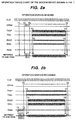
- Fig. 2 shows an example of a timing chart which is divided into during sending (a) and during receiving (b).
- the DSP 3 controls the I/O 37 according to an instruction from a terminal first and turns the DC loop control signal OFHK off (T1).
- the line that is, the switchboard
- the line interface circuit 2 sends a dial signal. This is executed by turning the OFHK terminal ON or OFF according to the line standard and turning the DC loop ON or OFF. For example, in Japan, it is 10 PPS (pulse per second) or 20 PPS.
- the terminal waits until the line is connected to the remote modem (T4), activates the modem 1, and starts sending.
- the modem 1 generates sending signals TXA+ and TXA-via the SOR 35 of the DSP 3 and the DA converter 41 of the AFE 4 according to the predetermined procedure and starts up communication with the remote modem.
- the line interface circuit supplies the TXA signal to the 2-wire - 4-wire conversion circuit 71 via the sending path 61 of the insulating coupler 6.
- the 2-wire - 4-wire conversion circuit 71 reduces turning to the receiving side and sends the sending signal to the line from the TIP and RING terminals via the DC loop circuit 81.
- the remote modem When the remote modem responds to this sending signal (T5), the signal of the remote modem can be seen on the line, and the receiving signal is selected by the 2-wire - 4-wire conversion circuit 71 via the reverse path, transferred to the modem 1 via the receiving path 62 of the insulating coupler 6, the AD converter 42 of the AFE, and the SIR 36 of the DSP 3, and amplified, filtered, and demodulated by the signal process of the DSP, and the digital data is restored and transferred to the host as received data.
- the terminals send and receive their stop information by the protocol which is upper than that of the modem signal and then output a stop instruction to the respective modems (RS off) and each modem stops the signal in response to it (T6, T7). Then this communication ends (T8), OFHK is turned off.
- a signal roughly like the one "between TIP and RING" shown in Fig. 2 appears between the line connection terminals TIP and RING in correspondence with each timing from T1 to T8.
- the modem During receiving, the modem is activated by the RING signal from the line side (T1) and when the line interface circuit detects it by the RING detection circuit 82, it immediately transfers it to the modem 3 via the Rdet path 64 of the insulating coupler 6.
- the modem 3 becomes aware of it through the I/O circuit 37 and when the modem 3 responds to it, it outputs the DC loop control signal OFHK in the same way as with during sending and loops the DC (T2).
- the switchboard of the office stops the RING signal (T3), so that the remote modem sends a modem signal after waiting for the decided time of the line (T4).
- the modem 3 receives it as signals RXA+ and RXA- and when the receiving side modem recognizes it as a modem signal, it responds to it and starts sending (T5). Also when the communication is to be completed, it ends by almost the same sequence as that during sending such as T6, T7, and T8. During these receiving operations, the signal shown in the drawing (schematically indicated) appears on the line in correspondence with each timing from T1 to T8. This operation itself is generally as specified in the standard.
- Fig. 3 is a circuit block diagram of one path of the insulating coupler 6 in the embodiment shown in Fig. 1.
- numerals 9-1 and 9-2 indicate capacitive insulating barriers which will be described later, 21 an input circuit, and 22 an output circuit and a safety boundary between the terminal of the modem and the switchboard is realized by the insulating barriers.
- the input circuit 21 inputs power and a signal from a terminal 103, comprises a modulation circuit 104, a drive circuit 105, and a protection circuit 106, converts and modulates an inputted analog signal, converts it to a PWM (pulse width modulation) signal, and outputs the signal to the output circuit 22 via the insulating barriers 9-1 and 9-2.
- PWM pulse width modulation
- the output circuit 22 comprises a protection circuit 107, a detection circuit 108, and a demodulation circuit 109, supplies power from a terminal 110, detects a signal sent from the insulating barriers 9 by the detection circuit 108, reproduces a PWM signal from the detected signal by an integration circuit 135 and a comparison circuit 137, and reproduces an analog signal corresponding to the input signal from the PWM signal.
- the output circuit 22 also has a function for extracting a timing signal from the detected signal and outputting these signals.
- the terminal 103 on the input side includes power terminals VDD1 and VDD2, a grounding terminal VSS1, and a clock input terminal for differential input of + and - as signal input and modulation timing.
- the modulation circuit 104 comprises a comparison circuit 111 and a carrier generation circuit 112.
- the drive circuit 105 is an inverter driver comprising PMOS transistors 113 and 114 and NMOS transistors 117 and 118.
- the protection circuit 106 comprises diodes 121, 122, 123, and 124 and resistors 129 and 130 and prevents circuit breakdown due to approaching of a surge voltage from the side of the output circuit 22.
- the protection circuit 107 on the side of the output circuit 22 comprises resistors 131 and 132 and diodes 125, 126, 127, and 128 and protects the gates of the transistors of the detection circuit 108.
- PMOS transistors 115 and 116 and NMOS transistors 119 and 120 constitute a detection circuit of an inverter constitution having feedback resistors 133 and 134.
- the output of the detection circuit 108 is connected to the integration circuit 135.
- the integration circuit 135 reproduces a PWM waveform from an inverter output signal.
- Numeral 136 indicates a circuit for reproducing the timing of a carrier and 137 indicates a comparison circuit.
- the terminal 110 on the output circuit side supplies power from power terminals VDD3 and VDD4 and a grounding terminal VSS2 and outputs the signal outputs + and - of a complementary type of processing results and the timing clock.
- the characteristics of this constitution are (1) the two insulating barriers 9-1 and 9-2 are used, and (2) an external clock is inputted, and (3) a reproduced clock is outputted.
- an input protection circuit is installed when they are to be independently used as an insulating coupler.
- a combination of PMOS and NMOS is indicated.
- the bipolar process or coexistence process may be used.
- a clock may be internally generated.
- Fig. 4 is an operation timing chart of the insulating coupler shown in Fig. 3 and the signal transmission system is the PWM (pulse width modulation) system.
- a carrier sufficiently higher (1.2288 MHz, 256 times or more in this case) than the frequency band (about 3.4 kHz max. in this case) of an input signal having a waveform to be transferred is used, and the time axis is divided for each fine period T, and an input signal at each time is transmitted by converting the magnitude thereof to each pulse width t.
- an input signal is differentially inputted such as input signal + and input signal -.
- another input system may be used.
- Fig. 4 schematically shows a sine wave when it is applied to the + and - input terminals.
- the rectangular clock inputted from outside the insulating coupler is converted to a saw tooth waveform by the carrier generation circuit 112 and used as a carrier.
- the modulation circuit 104 is the comparison circuit 111 and outputs the PWM + and PWM - waveforms in which the pulse duty is changed by receiving these input signals.
- the drive circuit 105 inputs the PWM + and PWM - waveforms to the drive circuit 105 and supplies them to the one-side terminals of the insulating barriers 9-1 and 9-2 via the protection circuit 106.
- the capacitor values of the insulating barriers 9-1 and 9-2 are about 1 pF.
- the protection circuit 106 is set at a constant such that it is effective in a high voltage surge waveform of several tens ns or less, so that it will hardly affect this drive waveform.
- the other electrodes of the insulating barriers 9-1 and 9-2 input to the detection circuit 108 via the protection circuit 107.
- This detection circuit 108 is the inverter and integration circuit 135.
- the inverter output has a differential waveform like those of the detection signals + and - and is extremely attenuated due to the stray capacity, so that it is amplified by the inverter once and inputted to the integration circuit 135.
- the integration circuit 135 is an integrator having two input terminals of + and - and inputs a signal in a differential waveform, so that it outputs reproduced PWM signals + and - as shown in the drawing.
- the timing reproduction circuit 136 is a PLL circuit and extracts the timing signal component from the reproduced PWM signal. When a saw tooth waveform is generated using the timing waveform and it is subjected to sample-holding at the timing of the reproduced PWM signal, a demodulated waveform like the output signals + and - can be reproduced.
- the modulated waveform may be a triangular wave.
- the center timing of the modulated waveform becomes constant, so that for example, there is an effect that a high precision timing reproduction system like PLL can be used in the demodulation circuit.
- a flip-flop of a set-reset type may be arranged in place of the integration circuit.
- the startup timing of a differential waveform which is an inverter output is the PWM timing information itself and by properly selecting the characteristics of the load resistor and inverter, it can be used as a flip-flop control signal as it is.
- the output of the flip-flop is the PWM waveform itself.
- the characteristic of this operation timing is that the three control signals of sending signal, receiving signal, and line connection control signal are transferred in parallel. As a result, in a line interface using this insulating coupler, the crosstalk of a signal becomes noise and the SN ratio is degraded. Therefore, in this embodiment, the DSP operation timing, modem processing timing, and insulating coupler timing are synchronized and this degradation is suppressed. This will be explained by referring to Fig. 5.
- Figs. 5(a) and 5(b) show the relationship between the modem signal process and the insulating coupler operation timing.
- the characteristic of the circuit constitution of this embodiment is that the operation timing of the line interface circuit is supplied from the modem and the circuit operation in the IC is synchronized with this clock.
- (a) shows the modem signal processing portion and although the timing chart is schematic, the relationship is shown on the right side of the chart. Namely, in the mode signal processing portion, the DSP operates at 39.3216 MHz, and 1.2288 MHz is supplied to the AFE and used as DA conversion timing MCLKS and AD conversion timing MCLKR.
- the DA conversion and AD conversion system is a 256-times over sample system, so that the substantial value is 9.6 ksps.
- (b) shows the clock timing relationship of the line interface portion and the clock signal DSPCLK supplied from the DSP is supplied to the sending signal path 61 of the insulating coupler 6 and the control signal path 63 as NCLKS and synchronized with the modem operation timing. It is desirable that the receiving signal path NCLKR operates only when the control signal is in the ON state, so that it has a gated waveform as shown in the drawing. Although the timing CLK2 of the Rdet path is locally generated in the line side circuit, it is stopped by the control signal OFHK during sending and receiving of a signal between the modems.
- FIG. 6 shows the PWM modulation timing when the saw tooth waveform is used as a carrier.
- modulation a saw tooth waveform changing to a carrier waveform by integrating a clock signal is generated and a PWM modulated waveform is obtained by comparing it with a transmitting signal.
- the receiving signal, sending signal, and OFHK control signal are shown.
- the receiving signal is affected by the transmission loss on the line as shown in RXA + and - in Fig. 1, so that the amplitude is small such as from -20 to -45 dBm or so.
- the sending signal is sent by itself, so that the amplitude is large, generally from -6 to -15 dBm or so.
- the control signal is at a logic level of 5 V, showing a maximum value. Then these amplitudes are converted to PWM duty, as shown in the drawing, the signal with a small amplitude deflects in a narrow width and the signal with a large amplitude deflects in a large width.
- the modem waveform is an AC signal, so that the deflection can be seen as shown in the drawing and the control signal is seen as if it is stopped.
- the timing of each insulating coupler is synchronized, so that as shown in Fig. 6, the carrier waveform, modulated waveform, and PWM waveform of the control signal are lined up and the mutual interference is minimized.
- a sending or receiving signal is converted from analog to digital or from digital to analog at the predetermined timing.
- the effect can be minimized (in the asynchronization, there is an effect of beat noise).
- the PWM waveforms are overlapped and the rising and falling positions approach each other, so that mutual interference that the noise generated in the self circuit by the operation of the self circuit affects the operation of another circuit by an electric connection of the devices and circuits and disturbs the rising and falling timings of another circuit, so-called crosstalk is generated.
- the PWM insulating coupler is used for analog data transmission, a waveform distortion is generated by this disturbance and the S/N ratio of the transmission signal is degraded by this distortion. Therefore, for example, in a sound signal, noise increases and in modem application, a transmission error occurs.
- Fig. 6(b) shows the PWM modulation timing when the principle is applied to a triangular waveform carrier.
- the same problem is basically included.
- the same effect can be obtained. Since the clock for the insulating coupler 105 for transferring the termination detection signal Rdet is generated by the oscillator OSC 112 arranged on the line side, it does not match with the operation of another insulating coupler in timing. However, since the oscillation is inhibited when the OFHK control signal is inputted and the operation of the oscillation circuit is stopped by this action before the modem communication starts, there is an effect that the effect of crosstalk can be suppressed by it.
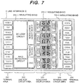
- Fig. 7 is a conception diagram of layout of this line interface IC.
- numeral 2 indicates a line interface IC and 206-1, 206-2, and 206-3 indicate insulating bands and enclose a line side terminal area 201, a line side circuit area 202, a terminal side circuit area 204, and a terminal area 205 respectively.
- Numeral 203 indicates the four insulating couplers shown in Fig. 1 which are arranged in one row in the insulating coupler arrangement area.
- the characteristics of this layout are (1) four insulating couplers using capacitive insulating barriers are used, (2) the line side circuit and the terminal side circuit are geometrically arranged so that they are separated with the insulating couplers lying between them, and (3) each of the line side circuit and terminal side circuit is enclosed by an insulating band.
- the insulating band has advantages that the circuits on the line side and terminal side are insulated and separated respectively by it, and the inside of each area can be freely designed without taking the dielectric strength between the primary circuit and the secondary circuit into account, and the evaluation and management of the insulating capability are simplified at the same time.
- Fig. 8(a) is a plan view
- Fig. 8(b) is a cross sectional view, and both drawings schematically show only the drive circuit and detection circuit.
- numeral 203 indicates an insulating coupler area
- 206 an insulating band
- 207 an insulating barrier
- 211 an input circuit area
- 212 an output circuit area.
- the insulating band 206 forms many patterns of 206-1 to 206-6.
- the portion codes of the insulating barrier 207 are partially omitted because they are complicated but they are the same.
- the input circuit area 211 and the output circuit area 212 further comprise PMOS areas 213, 214, 215, and 216 and NMOS areas 217 and 218.
- As input terminals of the input circuit two inverter input terminals IN1 and IN2 of the drive circuit are indicated.
- As output terminals of the output circuit two inverter output terminals OUT1 and OUT2 of the detection circuit are indicated.
- VDD1 to VDD4 indicate separated power terminals and VSS1 and VSS2 indicate separated grounding terminals.
- the characteristics of the plan view (a) are (1) the circuit area is separated by the insulating bands, (2) with respect to the insulating barrier, the insulating bands are formed in a pattern of teeth of a comb so as to reduce the opposed area, and (3) four capacitors are horizontally connected in series so as to form two sets of insulating barriers. These are driven in a complementary PWM digital waveform as mentioned above. There is little crosstalk between the two sets of insulating barriers. However, in the case of a use in which it is questionable, it is effective to provide a long space, a power pattern VDD, and a VSS wiring pattern between the two sets of insulating barriers, that is, horizontally and arrange them between the insulating barriers so as to loose the connection.
- numeral 231 indicates a substrate, 232 an insulating layer, 233 a semiconductor layer, and 234 a protection layer, and the semiconductor area is formed by many insulating bands 206, and the input circuit area 211, the insulating barrier 207, and the output circuit area 212 are arranged from the left.
- a silicon wafer (SOI substrate) having an insulating layer of SiO 2 with a thickness of about 2 microns as an inner layer is prepared and each area is formed on it using the thin-film process using a photo mask.
- the insulating bands 206-1 to 206-6 are SiO 2 layers with a width of about 1.5 ⁇ m.
- the areas such as the input and output circuit areas and insulating barrier area are divided and formed by the insulating bands 206 on a silicon wafer having an insulating layer as an inner layer and furthermore the protection layer 234 is overlapped on them.
- the silicon wafer has a constitution that one SiO 2 layer or a multi-layer comprising a polysilicon layer having an oxidized surface overlapped on the aforementioned SiO 2 layer is overlapped on the substrate 231 of single crystal silicone and furthermore a semiconductor layer of single crystal silicone is overlapped on it.
- a method that the surface of a silicon oxide film on the polysilicon surface is mirror-polished and overlapped and then joined by heat treatment at a specified temperature is used.
- the insulating bands 206 are SiO 2 layers and insulators.
- the protection layer 234 is an insulator of SiO 2 and HLD or SiN and includes a wiring layer using polysilicon or aluminum.
- the insulating bands 206 are formed by a method for cutting a trench once and filling it with SiO 2 or BPSG, a method for thinly oxidizing the side wall of a trench and filling it with polysilicon, a method for coating PIG or SOG, or a method for changing a semiconductor layer to an insulator by irradiating oxygen ions from the top.
- the capacitor comprises three electrode areas 236, 237, and 238 and the insulating band 206. By doing this, even in the trenching system that the insulating band 206 is limited to the width compared with the thickness of the insulating layer 232, the dielectric strength can be reserved by connecting the capacitor in series.
- Numerals 235 and 239 indicate the sections of the input circuit area 211 and the output circuit area 212 and these are enclosed by two insulating bands and structured so as to obtain high dielectric strength. Since a plurality of circuits are physically insulated from the substrate by the insulating bands and insulating layer in this way, there is an advantage that this integrated circuit can be directly bonded to the frame during package mounting, hence the heat dissipation is satisfactory.
- FIG. 9 (a) is a plan view and (b) and (c) are the cross sectional views A-A' shown in the plan view (a).
- numeral 207 indicates an insulating barrier, 206-1, 206-2, and 206-3 insulating bands of SiO 2 with a thickness of about 1.5 microns, 241, 242, and 243 electrode areas enclosed by the insulating bands 206, and 244 and 245 terminals which are holes made in the protection layers on the upper parts of the electrode areas 241 and 242.
- numeral 231 indicates an Si substrate with a thickness of about 400 microns, 232 an insulating layer with a thickness of about 2 microns, 233 a semiconductor layer with a thickness of about 15 microns, and 234 a protection layer with a thickness of about 5 microns and the other numerals are the same as those shown in (a).
- each area is formed using the thin-film process using a photo mask.
- the insulating band is an SiO 2 layer and an insulator.
- the insulating bands 206 are formed by a method for cutting a trench once and filling it with SiO 2 or a method for changing a semiconductor layer to an insulator by irradiating oxygen ions from the top.
- the capacitor comprises the three electrode areas 241, 242, and 243 and the two insulating band 206-1 and 206-3.
- the insulating bands are patterned by folding each band as shown in the drawing and the capacity can be efficiently obtained with a small semiconductor area by making the contact portion of the electrodes 241, 242, and 243 longer.
- the insulation performance is obtained that the capacity is about 2 pF for a square of about 160 microns and the dielectric strength is about 750 V for each insulating band in the DC withstand voltage test.
- a high voltage is applied between the terminals 244 and 245 and as viewed from the outside of the insulating barrier 207, a pattern that the electrode areas 241 and 242 are doubly enclosed by the insulating bands is obtained.
- a circular pattern (a radius of 2 to 5 microns) is used for the portions to be folded and the angles as far as possible so as to prevent a sharp pattern.
- the portion of the insulating band 206-2 is necessary so as to insulate and separate from the other circuit portions.
- Fig. 9(c) is a structural diagram when each insulating layer cannot be made thicker and by use of two insulating layers, the effective dielectric strength can be increased. In an IC of a multi-layer structure, a considerable warp can be seen. However, by using an insulating multilayer and adjusting the thickness of each layer, an effect is obtained that the stress is dispersed and the warp is reduced.
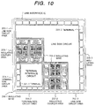
- Fig. 10 is another layout conception of a line interface IC and as shown in the drawing, respective two insulating couplers are perpendicularly arranged.
- a test voltage of 1500 VDC is applied between the line side circuit and the terminal side circuit.
- the circuit areas are enclosed and arranged by the insulating bands respectively on the SOI substrate, a considerably free layout is available.
- the layout is restricted by wiring between the areas and arrangement and size of terminals.
- This layout is characterized in that when the circuit areas and the number of terminals are unbalanced, the areas can be efficiently arranged.
- Fig. 11 various transmission methods from (a) to (f) are shown using block diagrams.
- the insulating barriers are the capacitors of the present invention.
- the insulating coupler of the present invention uses two insulating barriers and is driven by a complementary waveform so that a signal can be precisely transmitted even if the receiver side is floating.
- the input circuit is supplied with power from the power terminal VDD1 and the grounding terminal VSS1 and converts and outputs the signal received from the input terminal to the waveform for driving one terminal of the insulating barrier.
- the output circuit is supplied with power from the power terminal VDD2 and the grounding terminal VSS2, detects the waveform appearing at the terminal on the opposite side of the insulating barrier, and converts and outputs it to an output signal.
- various methods such as the PWM (pulse duty conversion) system for digitizing only the amplitude direction, or the FM system (voltage - frequency conversion) system, or the digital transmission system for also digitizing the time base direction can be used.
- Fig. 11(b) shows a case of the PWM transmission system.
- the input circuit samples the inputted analog signal in the fixed period T more than several tens times of the signal band and converts and transmits the amplitude to the duty (0 volt input corresponds to 50% duty) in the time base direction and the output circuit detects it and converts the duty to an amplitude value once again, hence reproduces the input waveform, and outputs an analog signal.
- the output circuit detects it and converts the duty to an amplitude value once again, hence reproduces the input waveform, and outputs an analog signal.
- a digital signal may be transmitted.
- Fig. 11(c) shows a case of digital transmission of the present invention.
- the code conversion is executed, for example, like the Manchester code so that the same level is not continued in the transmission waveform, and then the insulating barrier is driven, and the output circuit detects it, reversely converts it, and reproduces the original digital signal.
- the code conversion and reverse conversion are executed. This method is characterized in that since little conversion is executed in the amplitude direction, it is hard to be affected by noise.
- Fig. 11(d) shows a case that AD conversion input is executed via the insulating barrier.
- the input circuit converts an analog input signal from analog to digital, then performs the same code conversion as that of (c), and drives the insulating barrier.
- the output circuit detects it, performs reverse code conversion, and then outputs a digital signal.
- Fig. 11(e) shows a case that DA conversion output is reversely executed via the insulating barrier.
- the input circuit performs the same code conversion as that of (c) for a digital input signal and then drives the insulating barrier.
- the output circuit detects it, performs reverse code conversion, converts it from digital to analog, and then outputs a digital signal.
- Fig. 11(f) shows a case that (d) and (e) are combined and input and output of an analog signal are executed by use of AD conversion and DA conversion.
- the signal transmission system from (d) to (f) is a constitution suitable for the sound signal processing analog front end of a modem and the line interface when the DSP is selected as a connection destination of a digital signal.
- the aforementioned capacitive insulating barrier is a circuit for connecting two circuits
- the stray capacity between the insulating barrier and the substrate is large and greatly different from that when the input circuit, output circuit, and insulating barrier are separately created and combined. Therefore, the transmission efficient by the insulating barrier is low such as 1-severalth.
- the amplifier circuit in the first stage of the output circuit, the amplifier circuit is arranged and the detection process and demodulation process are performed behind it.
- Fig. 12 is a circuit block diagram of the modem device of another embodiment of the present invention.
- numeral 251 indicates a line interface IC of this embodiment, 252 a terminal side circuit, 253 an insulating coupler, 254 a line side circuit, and 255 a highly dielectric circuit.
- the terminal side circuit 252 comprises a DSP interface 256, a modem data output interface SOR 261, a modem data compression circuit 262, a sending side multiplexer 263, a master register GORM 264 of a general purpose output register, an error correction circuit 265, a receiving side multiplexer 266, a receiving modem data expanding circuit 267, a modem data input interface SIR 268, a general purpose input data error correction circuit 269, and a slave register GIRS 270 of a general purpose input register.
- the insulating barrier 253 comprises a sending path insulating coupler 6-1 and a receiving path insulating coupler 6-2
- the line side circuit 254 comprises a multiplexer 271 of a line side sending path as a sending path, a sending modem data expanding circuit 272, a DA converter 273, a general purpose output data error correction circuit 274, a slave general purpose register 275, an AD converter 276, an AD conversion data compression circuit 277, a multiplexer 278, a master general purpose input register GIRM 279, an input data error correction circuit 280, a 2-wire - 4-wire conversion circuit 281, and a switch control circuit 283, and the highly dielectric circuit 255 comprises a DC loop circuit 282 and a call signal detection circuit 284.
- the first characteristic of this circuit constitution is that the AD converter and DA converter are arranged on the line side and a signal passing the insulating coupler is digital data. As a result, as described later, the noiseproof performance when a signal passes the insulating barrier is greatly improved.
- the second characteristic is that an AD conversion signal and a DA conversion signal are compressed once and pass through the insulating coupler, and a control signal is coded for error correction and positioned in this empty portion, and the insulating couplers 6 are reduced by half such as 6-1 and 6-2.
- the third characteristic is that the circuit constitution is functionally the same as that shown in Fig. 1 and the internal circuits of the highly dielectric circuit 255 and the 2-wire 4-wire conversion circuit 281 and switch control circuit 283 of the line side circuit 254 have the exactly same functions.
- the fourth characteristic is that the multiplexer 266 inputs both the reproduced clock of the insulating coupler 6-2 and the clock from the DSP and adjusts the timing. When a 1-bit or 2-bit buffer memory is arranged, the timing can be adjusted.
- the fifth characteristic is that the general purpose input and output registers GOR and GIR successively transfer contents of the master register to the slave register. Needless to say, as deformation of this circuit, if the art makes progress and the insulating coupler becomes smaller, when the noise reduces and data is not easily mistaken, compression, error correction, and the multiplexer may be omitted.
- FIG. 13 shows a case that a saw tooth waveform is used as a carrier and (b) shows a case that a triangular wave is used as a carrier. Even if a sending signal and a receiving signal are analog signals as shown in both drawings, only a digital PWM signal passes through the insulating barrier and the operation timings of the DSP, modem process, and insulating coupler are synchronized, so that the performance can extremely withstand a transmission error by the insulating barrier.
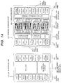
- Fig. 14 shows a case that the line interface IC comprises two chips.
- numeral 291 indicates a line interface chip and 292 indicates a terminal interface chip.
- a terminal area 293, a line side high voltage circuit area 294, and a terminal area 295 are arranged and in the terminal interface chip 292, a terminal area 296, a line side low voltage circuit area 297, an insulating coupler area 298, a terminal side circuit area 299, and a terminal area 300 are arranged.
- a DC loop circuit and a termination (RING) detection circuit are arranged in the line side highly dielectric circuit area 294.
- a 2-wire - 4-wire conversion circuit In the line side low voltage circuit area 297 of the terminal interface chip 292, a 2-wire - 4-wire conversion circuit, an OFHK switch (SW) control circuit, and an originating circuit are arranged.
- SW OFHK switch
- the terminal interface chip receives only a logic signal and a signal at the modem signal level and the portion to be directly connected to the line is eliminated, so that an effect is produced that the application range can be easily spread such as application to other than the modem, for example, use as an internal circuit of a multifunction telephone set.
- Fig. 15 is a structural diagram of another embodiment of the insulation barrier, and (a) is a plan view of single insulation, and (b) is a plan view of double insulation, and (c) is a plan view of another deformed embodiment of double insulation.
- numeral 207 indicates an insulating barrier, 206-1, 206-2, and 206-3 insulating bands, 241 and 242 electrode areas enclosed by the insulating bands 206, 244 and 245 terminals which are holes made in the protection layers on the upper parts of the electrode areas 241 and 242, and 301-1 and 301-2 partitions.
- Figs. 15(a) and 15(b) show embodiments of patterns of insulating bands having no acute angles at all in the same way as those of the embodiment shown in Fig. 9.
- the characteristic of the pattern shown in Fig. 15(a) is that the electrode areas 241 and 242 having the terminals 244 and 245 are formed by drawing with a single stroke of the pen by the insulating bands 206-1 and 206-2. By doing this, the portion where the insulating bands are in contact with each other in a T shape can be eliminated and there is an effect that not only the filling efficiency in a groove by the trench method is satisfactory but also the concentration of the electric field is reduced. The same may be said with Fig.
- the electrode areas 241 and 242 having the terminals 244 and 245 are formed by drawing with a single stroke of the brush by the insulating bands 206-3 and 206-4 and these are further enclosed by the insulating bands 206-1 and 206-2 respectively.
- intermediate electrodes are formed between the insulating bands 206-1 and 206-3 and between the insulating bands 206-3 and 206-4, so that there is an effect that two times of dielectric performance can be realized.
- the pattern shown in Fig. 15(c) is a deformation example of the embodiments shown in Figs.
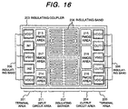
- Fig. 16 is a structural diagram of an embodiment of the insulating coupler of the present invention.
- An insulating coupler 203 shown in Fig. 16 is structured so that a terminal area 201 for the input circuit and a terminal area 205 for the output circuit are provided in the portion of the insulating coupler shown in Fig. 8 and the respective terminals are arranged and the size thereof is a square of about 2 mm.
- a micro-monolithic insulating coupler part of the analog PWM system can be produced.
- the part is certainly mounted on a package in the later process, it is very small because it is monolithic. Therefore, it is mounted within an application device such as a probe of a measuring instrument and various medical sensors and can contribute to miniaturization and high performance of these devices.
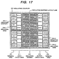
- Fig. 17 is a layout structural diagram when the two insulting couplers shown in Fig. 16 are mounted on one chip.
- numeral 203 indicates a 1-chip insulating coupler containing two couplers and 203-1 and 203-2 indicate a built-in insulating coupler 1 and insulating coupler 2 respectively and are enclosed by insulating bands 206-1 and 206-2 respectively.
- the characteristics of this layout are (1) each insulating coupler is enclosed by insulating bands 62-1 and 62-2 and (2) the insulating barriers in which the electric field is concentrated are lined up. By doing this, the dielectric strength can be secured between any of two inputs and any of two outputs and there is an effect that each circuit device can be freely arranged with the dielectric strength maintained. By use of this structure, an unnecessary electric circuit connection can be minimized and the application range can be spread.
- Fig. 18 is still another embodiment of the insulating coupler of the present invention and shows the structure of an integrated circuit and insulating coupler when an input circuit and output circuit insulated by insulating bands respectively are structured as integrated circuits and an insulating coupler is formed by combining a ceramic capacitor and an insulating barrier.
- (a) shows an outline of chip layout and (b) shows a cross sectional view when the IC and ceramic capacitor are mounted on a circuit substrate.
- Fig. 18 shows an outline of chip layout and (b) shows a cross sectional view when the IC and ceramic capacitor are mounted on a circuit substrate.
- numeral 303 indicates an insulating coupler IC, 206-1 and 206-2 insulating bands enclosing the input circuit area and output circuit area respectively, and 304 an external insulating barrier and terminal areas 201 and 205 include connection terminals "C1-O and C2-O" and "C1-I and C2-I” with the external insulating barrier 304 respectively.
- the other numerals have the same meanings as those shown in Fig. 16.
- numeral 303 indicates an insulating coupler IC and 305 and 306 indicate solder.
- Numeral 307 indicates a circuit substrate having a circuit connection pattern of copper leaf 308, 309, 310, and 311 on both sides and through holes 312 and 313 are provided as required.
- the circuit substrate 307 may be a multilayer of copper leaf as required unless the insulating property is damaged.
- An insulating barrier 304 is a chip capacitor and mounted on the surface of the circuit substrate with the solder 316 and 317. By doing this, the insulating barrier occupying a comparatively large area in the semiconductor integrated circuit is mounted as another chip and the size of the insulating coupler increases.
- the capacitor value of the insulating barrier is positively increased, and the operation timing frequency can be freely selected is made possible.
- the low frequency characteristic is improved by increasing the capacitor value, so that there is an advantage that the waveform can be easily transmitted and for example, small power also can be transferred by a charge pump circuit.
- an insulating coupler can be reasonably formed on a semiconductor integrated circuit and the use of an integrated circuit can be widely spread.
- the insulating coupler formed in this way has an effect that it greatly contributes to miniaturization and low price.
- Fig. 19 is a structural diagram showing the concept of an embodiment that the monolithic line interface of the present invention is applied to a card modem device.
- Fig. 19(a) shows an embodiment of the present invention and
- Fig. 19(b) shows a conventional card modem.
- numeral 400 indicates a whole card modem of this embodiment, 401 a circuit substrate of this embodiment, 402 a line interface IC of this embodiment, 403 an AFE, 404 a DSP, 405 other ICs, 406 a line side connector, 407 a PC side connector, 408 a varister, 409 a highly dielectric capacitor, 410 a capacitor, and 411 to 416 chip parts such as other resistors and capacitors.
- Fig. 19(a) shows an embodiment of the present invention
- Fig. 19(b) shows a conventional card modem.
- numeral 400 indicates a whole card modem of this embodiment, 401 a circuit substrate of this embodiment, 402 a line interface IC of this embodiment
- numeral 450 indicates a conventional whole card modem, 451 a conventional circuit substrate, 452 a line transformer which is a conventional line interface, 453 an AFE, 454 a DSP, 455 other ICs, 456 a line side connector, 457 a PC side connector, 458 a varister, 459 a highly dielectric capacitor, 460 a capacitor, and 461 to 466 chip parts such as other resistors and capacitors.
- This drawing shows the section of the card modem which is schematically indicated and the comparison shows that in the conventional card modem 450, the circuit substrate 451 is hollowed out and the line transformer 452 is arranged in the hollowed portion, while in the embodiment of the present invention, the line interface IC 402 can be mounted almost in the sane way as the other ICs shown in from 402 to 405. Therefore, it is not necessary to hollow the circuit substrate 401 and the present invention is economical. Since a special transformer is not used, there is the possibility that the constitution can be made economical. Furthermore, since the transformer can be omitted, there is a possibility of further miniaturization.
- Fig. 20 is a circuit block diagram of an embodiment when the monolithic digital insulating coupler of the present invention is applied to an AFE.
- the AFE of this embodiment is used for processing a voice band signal and performs oversample (2 MHz) AD and DA conversion as analog and digital conversion, reduces the speed to 32 ksps once by a decimeter filter and interpolator, furthermore performs the low pass filtering process by the internal DSP, and finally inputs or outputs digital data at a speed of 8 ksps.
- I-AFE 500 indicates a monolithic analog front end (I-AFE) containing digital insulating couplers 501 to 506.
- the I-AFE 500 comprises an analog input line including a multiplexer (MUX) of the original AFE, a pad amplifier (PDA) 512, a prefilter (PF1) 513, an oversample analog to digital converter ADC 514, a decimeter filter (DCM) 515, an AD conversion output buffer (ADCR) 516, a built-in (in-) DSP 517, and a receiving output buffer (RXDR) 518, an analog output line including a sending buffer (TXDR) 521, a DA conversion input buffer (DACR) 522, an interpolator (INT) 523, an oversample digital to analog converter DAC 524, a post filter (PF2) 525, and an attenuator (ATT) 526, data I/O transfer controllers 531 and 532 of the in-DSP 517, and a 2-wire
- the inside of the I-AFE 500 is reset or controlled in power down by a control circuit (CONT) 541.
- a reset signal is transmitted to the circuit on the left (hereinafter referred to as the analog I/O side) via the digital insulating coupler 506, combined with a reset signal following power ON or OFF on the analog I/O side by a reset circuit 542, and used as a reset signal for the circuit on the analog I/O side.
- an external device uses control registers (CONTR) 551 and (STATUS) 554.
- the content of the CONTR 551 (STATUS' 553) is copied into the control registers (CONTR') 551 and STATUS 554 of the analog (digital) I/O circuit via the digital insulating couplers 504 and 503 and controls SW1 to SW3 of the analog I/O side circuit and other circuits and sets the level of a general purpose output port (GPO).
- the operation timing of the I-AFE 500 is converted to 8-fold 16 MHz by a 2-MHz clock (MCLK) PLL given by an external (ex-) DS0 536 and used as basic timing together with the inputted 2 MHz. Needless to say, it is also transmitted to the analog I/O circuit via the digital insulating coupler 505 and various timings are generated by a timing circuit 562.
- a reference voltage generation circuit 563 is a circuit for giving a reference voltage to the analog I/O circuit for operating by a single power supply and generates a reference voltage VREF of (VDD1 - VSS1)/2.
- the 2-wire - 4-wire conversion circuit 533 is a circuit for exchanging 2 wires of the pay station line and 4 internal sending and receiving wires when the I-AFE 500 is used in a mode device and has functions of line impedance matching and I/O amplification.
- An analog input signal is inputted via the 2-wire - 4-wire conversion circuit 533 or directly inputted from the IN+ and IN- terminals.
- the MUX 511 is switched and used by a signal SW1 beforehand according to one of them.
- the PDA 512 can switch the gains 0 dB and 6 dB by a signal SW2.
- the PF1 513 is an analog filter for deleting a signal of an unnecessary frequency band before performing AD conversion and a secondary low pass filter at a cut-off frequency 48 kHz in this embodiment.
- the ADC 514 is a secondary ⁇ modulator operating at 2 Msps and outputs an AD conversion result 2 bits long every 0.5 ⁇ s.
- the ADC 514 transmits this AD conversion output to the DCM 515 and thins it to 2 ksps.
- the output of the DF1 515 is 16 bit/w.
- the speed is slow such as 32 ksps, so that the DF1 515 serially converts it to 2 Msps and transmits it to the in-DSP 517 via the ADC 516 of the I/O side circuit together with the timing signal via the insulating coupler 502.
- the in-DSP 517 performs the flat characteristic correction for this decimeter output by the digital signal processes IIR and FIR and performs the LPF process at 4 kHz or less.
- the in-DSP 517 serially transmits the processing result to the ex-DSP 236 as 16-bit/w data for every 8 ksps via the receiving buffer 518.
- the analog output line receives the data (TXD) to be outputted from the ex-DSP 536 from the sending buffer TXDR 211 every 8 ksps, performs the same filtering process as that of analog input by the in-DSP 517, and transfers this result to the interpolation filter (INT) 523 at a speed of 32 ksps by interpolating it as 16-bit/w data via the DA output buffer (DACR) 522. Also in this case, the analog output line performs serial conversion and transmits the data via the insulating coupler 501. The INT 523 further performs the interpolation process, transfers it to the DAC 514 as 6-bit/w data at a speed of 2 Msps, and outputs an analog value.
- the loopback component remaining by the process by the in-DSP 517 and the INT 523 is removed by the post filter PF2 525 and outputted via the ATT 226 which can switch 0 dB, -6 dB, and - ⁇ dB.
- the timings of the analog input line are used.
- These processing timings are timings that the processing timing of the ⁇ modulator and demodulator of basically the sane timing among the 2-MHz timings, the interpolator and decimeter processing timing to be inputted and outputted at 2 Msps and 32 ksps, and the DSP processing timing to be inputted and outputted at 32 ksps and 8 ksps are allocated in order. Therefore, the analog I/O side circuit and digital I/O side circuit are separated by the insulating couplers 201 to 205. However, it is essential to synchronize and operate them and this is the reason why it is important to set an isolator only for timing.
- the I-AFE 500 viewed from the ex-DSP 536 is an I/O circuit of an analog signal and the sample timing is important. Therefore, in most modems, the sample timing of the ADC 514 is adjusted so that a most advantageous timing for discrimination and decision can be obtained during demodulation. Therefore, delay or advance of the timing is transmitted to the I-AFE 500 from the ex-DSP 536 by the clock MCLK. Namely, to advance the timing, ⁇ f is added and to delay the timing, - ⁇ f is added and the I-AFE 500 is informed of it. This process is performed every several tens ms or several hundreds ms.
- the I-AFE 500 When the I-AFE 500 operates at a selfish timing, it does not agree with the timing requested by the ex-DSP 536, so that data becomes too much or too little, and the processing time breaks down, and large noise is generated. To synchronize the I-AFE 500 with this clock delaying or advancing, the PLL is installed inside the I-AFE 500 so as to synchronize the internal timing. Needless to say, if the timing accuracy request permits, there is a complementary method available using the timing error of the automation means in the modem and in this case, the circuit timing adjustment is not executed.
- data transfer between the decimeter filter and interpolator and the in-DSP is serial high-speed transfer, so that there is an effect that the number of insulating couplers is decreased. Since the modem includes a plurality of standards, a plurality of sample timings may be requested. To respond to it, the division ratio of the PLL 561 and the timing circuit 562 can be controlled by the CONTR 562. Furthermore, by applying the aforementioned error correction means to the insulating couplers to which the control signal is transferred, the operation can be stabilized.
- a constitution that the digital filter is signal-processed by the internal DSP 517 is indicated.
- the process of the internal DSP is a dedicated process for AD conversion and DA conversion and these circuits may be formed by appropriate dedicated logic. When those circuits comprise dedicated logic, more economical integration may be realized.
- the two systems of analog input line and analog output line may be processed by one processing means.
- a whole 600 indicates the whole AFE integrated circuit and it is formed on an SOI substrate.
- An insulating band 601 is a means for insulating the analog I/O circuit area
- an insulating band 602 is a means for insulating the insulating couplers (indicated by isolators 501 to 506)
- an insulating band 603 is a means for insulating the digital I/O circuit area
- an insulating band 604 is a means for insulating between other chip areas on the wafer and the areas and the insulating band 604 is a means for preventing circuit connection with the substrate linking with the scribe end face.
- the names assigned to more finely divided areas in each area correspond to Fig. 20 respectively.
- the characteristics of this layout are that the circuit areas are further enclosed by trenches so as to form an analog I/O side circuit area 601, an insulating coupler area 602, and a digital I/O side circuit area 603, and (1) a double trench is formed between each areas so as to insulate between the areas, and (2) furthermore the whole is enclosed by a trench 604 so as to insulate between the chips.
- the trench 604 is a multitrench.
- each circuit block in the circuit areas 601 to 603 By enclosing each circuit block in the circuit areas 601 to 603 by a trench, the circuits are insulated and separated from each other and the devices are separated. However, when furthermore a multitrench is used and the trenches are grounded, a noise shield due to mutual interference can be formed.
- the insulation cooperation is taken into account so as to limit the destruction mode to the capacitor portion. By doing this, even if a high voltage more than the standard is applied, there is an effect that a system can be constructed with the damage limited.
- Fig. 22 is a circuit diagram of an embodiment of a DSP modem to which the I-AFE shown in Fig. 20 is applied.
- numeral 500 indicates I-AFE and 700 indicates ex-DSP.
- the modem is connected to a telephone line, it is connected to connection terminals TIP and RING via a protection circuit comprising resistors 701 and 702, capacities 703 and 704, and a surge protection device 705.
- Numerals 706 and 707 indicate switches formed by NMOS transistors and they are connected to a photo detector (for example, a solar cell) 708.
- the photo detector 708 receives light of a light emission diode 709, turn 706 and 707 on or off, and supplies power supplied via TIP and RING to the circuit on the right of the switches.
- the light emission diode 709 is controlled in light emission by the switch circuit comprising a transistor 710 and resistors 711 and 712.
- the control signal of this switch is POWER ON.
- Diodes 713, 714, 715, and 716 constitute a bridge and have a function for keeping the current direction constant regardless of the direction of the DC voltage applied to TIP and RING.
- the circuit comprising resistors 717 and 718, a capacity 719, transistors 720 and 721, a resistor 722, and an NMOS transistor 723 is a DC loop circuit, and when the control output terminal GPO of the I-AFE 500 goes high, the NMOS transistor turns on, and Darlington transistor circuits 720 and 721 operate according to the bias of the resistors 717 and 718 and flows a loop (looping) current balanced with the feedback resistor 722.
- the circuit comprising a resistor 724 and a 18-V Zener diode 725 is a protection circuit for preventing application of an excessive voltage to a 3-terminal regulator 726 and the I-AFE 500.
- a capacity 727 is a smoothing capacitor and capacities 728 and 740 are an output circuit of I-AFE and a signal connection capacitor.
- the POWER ON signal is generated first, and the NMOS switches 706 and 707 are turned on, and the 3-terminal regulator 726 is connected to the line, and a current is supplied to the AFE, and the GPO is put on the high level from the TXD via the CONTR next, and the NMOS switch 723 is turned on, and the loop current is conducted so as to notify the switchboard of the office that the modem is connected to the line.
- the modem sends a dial signal to the I-AFE 500 via the capacities 728 and 440 and waits until the switchboard connects the remote modem.
- the connected remote modem generates the normal modem signal, so that the modems mutually perform communication via the AFE hereafter.
- the capacity 729 and Zener diodes 730 and 731 are a sensitivity adjustment circuit for rejecting a response to an incoming signal at lower than the fixed voltage
- the resistor 732 is a current limit resistor of the diode 733 or the light emission diode 734
- the photo transistor 735 detects emitted light and notifies the modem 700 of it as a RING DETECT signal when an incoming signal flows in the light emission diode 734 through a load of the resistor 736.
- this signal is notified to the modem, and the POWER ON terminal responds to it, and the NMOS switches 706, 707, and 723 are turned on, and the loop current is conducted, and the power is turned on, and a modem response signal is repeated via the capacities 728 and 740.
- the modem signal is sent and received almost in the same way as that during sending.
- the first characteristic is that the analog I/O side circuit including the circuit of individual parts on the left of the arrangement of insulating couplers of the I-AFE all insulates the digital I/O circuit on the right. Conventionally, the circuit is insulated by an insulating transformer and if anything, located on the right. The transformer can be deleted by the I-AFE in this embodiment and a miniature modem device can be constructed.
- the second characteristic is that power is supplied to the analog I/O side circuit of the I-AFE from the office and the power is supplied. Therefore, it is not necessary to supply the power of the analog I/O device from the modem device side and it contributes to reduction in the whole power consumption.
- the third characteristic is that the switches of the individual part portion are divided into the POWER ON switches 706 and 707 and the loop current switch 723. By doing this, power is supplied to the AFE without conducting the loop current at start of line connection and for example, it can be used for sending and receiving a signal between the switchboard and the modem such as notification of the originating number.
- the insertion position of the insulating coupler in the AFE may be changed from that shown in Fig. 20.
- the insulating couplers are arranged between the ADC and DAC and the decimeter filter and interpolator.
- the data transfer speed in this portion is fast such as 2 bit/w ⁇ 2 Msps or 6 bit/w ⁇ 2 Msps, so that the insulating couplers are installed in parallel. Therefore, the delay time due to the transfer operation can be almost ignored.
- an echo canceller or the terminal is to be processed by the in-DSP, there is an advantage that the processing performance is little restricted compared with the case shown in Fig. 20.
- a charge pump circuit may be used as an ON-OFF control circuit for the NMOS switches 706 and 707.
- the charge pump circuit comprises a plurality of capacities, a driver for supplying electric charge to the capacities, and a plurality of switches for controlling electric charge supply and is a circuit such that by repeating an operation at high speed that electric charge is supplied to a capacity by the driver and switch and the electric charge is moved to another capacity by changing the switch, another capacity obtains a voltage.
- an ON-OFF control circuit can comprise only a silicon semiconductor device. Therefore, the ON-OFF control circuit can be integrated on the SOI substrate together with the I-AFE, so that the number of parts of the modem device can be decreased furthermore.
- insulating couplers to the AFE An application example of insulating couplers to the AFE is described above.
- 8 to 13 insulating couplers are used for the I-AFE, there is an effect that the area of chip layout can be made smaller such as less than 10% of the total area of the AFE.
- a constitution may be used that by operating and using insulating couplers at high speed of a multiple of the number of rows, the number of insulating couplers to be used is decreased. In either way, the effect of remarkable miniaturization is kept unchanged compared with a case that an insulating coupler using an insulating transformer and external highly dielectric capacitor is used. Since this integrated circuit is suited to mass production, it is also characteristic that the economical efficiency can be improved.
- a recent high speed modem requires high performance of a transformer, hence an expensive material such as permalloy is used as a core material, so that 2 or 3 fold part expenses are required compared with a case that an inexpensive silicon steel plate is used.
- this embodiment when this embodiment is applied, in the high-speed modem field, there is an effect that the present invention greatly contributes to not only miniaturization but also improvement of economical efficiency.
- a very miniature on-chip highly dielectric capacitor or a very miniature monolithic insulating coupler can be realized, and a miniature AFE can be realized by use of it, and a miniature and economical modem device can be realized by use of the AFE.
- Fig. 23 is a structural diagram of an embodiment of a communication system using a combination of a modem device and a host (PC).
- numeral 810 indicates, for example, the portion of the discrete circuit shown in Fig. 22 and it is a DAA (direct access arrangement) means including a protection device, connection switch, DC loop circuit, DC loop switch (DC loop), and call signal detection circuit.
- Numeral 811 indicates insulating, filtering, AD, and DA means like the I-AFE, 812 a modulation and demodulation means like the DSP, and 813 a transmission control means comprising an MPU, memory, and software and a modem section 800 comprises these units.
- Numeral 801 indicates an application control means such as a PC and it is a whole control CPU of the internal host CPU of the WS, PC, and PDA, the dedicated DSP, or the cluster modem and it is called a PC basic section or host here.
- Fig. 23(a) shows an embodiment using I-AFE in the constitution that the signal process is hierarchically divided among the DSP, MPU, and PC, so to speak, the conventional type modem constitution, and the expensive and large insulating transformer which is conventionally installed in the DAA is deleted by the I-AFE, and the number of photocouplers is decreased, and the embodiment contributes to miniaturization and improvement of economical efficiency.
- the monolithic insulating couplers are built in the AFE. However, they may be structured so as to combine with another part as required.
- the I-AFE and DSP may be integrated.
- Fig. 23(b) is a structural diagram of an embodiment of a soft modem device using I-AFE.
- each same numeral as that shown in Fig. 23(a) indicates the same name
- numeral 822 indicates an interface (I/F) means for connecting the modulation and demodulation means 811 and the application control means 803 and it includes a buffer memory about 0.5 MB long and another control logic circuit.
- the characteristic of this constitution is that by processing the modulation and demodulation means and transmission control means in a batch by the host CPU, the hardware of the modulation and demodulation means (DSP) 812 and the transmission control means (MPU) 813 is reduced and substantial miniaturization and improvement of economical efficiency of the modem device are realized.
- the monolithic insulating couplers may be combined with other than the AFE.
- the I/F means has a main function for temporarily storing AD and DA conversion data and if it is integrated with the I-AFE, the modem device can be miniaturized more.
- the I/F means 822 may be integrated with the application control means 803.
- the classification of the modem section is originally thin and the arrangement may be decided at the request of others.
- I-AFE that is, monolithic insulating couplers
- the insulating transformer can be deleted, and the number of photocouplers can be decreased, and miniaturization and improvement of economical efficiency of the equipment can be realized.
- Fig. 24 is a system block diagram of still another embodiment.
- numeral 850 indicates a controller, 860 to 862 insulating couplers, 851 a transceiver, and 852 a power regulator and these units constitute one station 840.
- Numeral 841 indicates another station whose inside is not disclosed and a plurality of other stations not shown in the drawing are assumed. These stations are connected to a network bus 870 including a signal bus 871, a power bus 872, a control signal bus not shown in the drawing, and a power supply 880 respectively in parallel.
- the controller and application circuit (controller side circuit portion) 850, the transceiver 851, and the power regulator 852 (network side circuit part) are insulated and separated by the insulating couplers 860 to 862 and the transceiver 851 connects the controller and application circuit 850 and the signal bus 871 via the insulating couplers 860 to 862 so that the network side circuit portion supplies power from the power bus 872.
- the insulating couplers connect the controller and application circuit 850 and the transceiver 851 and controls the standby operation of the transceiver 851.
- Fig. 25 is a layout diagram of insulating couplers corresponding to Fig. 16 when T-shaped or Y-shaped connection of an insulator is permitted as shown in Fig. 15(c) instead of drawing with a single stroke of the pen.
- numerals 201 to 207 indicate the same names as those shown in Fig. 16.
- An insulating band 206' has Y-shaped joints at the six circled portions and one input circle area, two insulating barriers, and one output circuit area are insulated and separated by the joints respectively.
- the insulator 206' is arranged in this way, for wiring between the input circuit and the insulating barriers and between the insulating barriers and the output circuit as shown in Fig. 16, there is an effect that there is no need to consider insulation between the area among the areas requiring to consider high insulation and the intermediate electrode area of the insulating barriers.
- Fig. 26 is a block diagram of a digital insulating coupler of an embodiment of the present invention.
- the primary circuit area, insulating barrier, and secondary circuit area are insulated and separated on one semiconductor substrate.
- Pls_in and Pls_out indicate an input pulse signal and output pulse signal of the insulating barrier respectively.
- Numeral 901 indicates a differential amplifier circuit for generating a complementary pulse signal on the basis of the input pulse signal Pls_in.
- Numeral 902 indicates a capacitive insulating barrier for coupling a complementary pulse signal driven by the differential amplifier circuit 901 to the secondary side with a high dielectric strength.
- Numeral 903 indicates a differential circuit for differentiating a signal coupled from the primary side by the insulating barrier 902.
- Numeral 904 indicates a transition detection circuit for inputting a pair of signals differentiated by the differential circuit 903 and detecting and amplifying each edge of the pair of differential signals.
- Numeral 905 indicates a pulse regeneration (demodulation) means for regenerating (demodulation) the input pulse signal Pls_in using an output signal of the transition detection circuit 904 and outputting the output pulse signal Pls_out.
- a digital insulating coupler is used because a signal is transferred from the primary side to the secondary side by a digital signal.
- an AD conversion circuit and a DA conversion circuit in the input section and output section of this embodiment, an analog insulating coupler can be easily realized.
- Fig. 27 is a concrete circuit diagram of a digital insulating coupler of an embodiment of the present invention.
- Fig. 28 is a drawing showing the operation waveform of the circuit shown in Fig. 27.
- the operation of the circuit of a concrete embodiment of the digital insulating coupler of the present invention will be explained by referring to Figs. 27 and 28.
- numeral 910 indicates a differential amplifier circuit for inputting an input pulse signal Pls_in and outputting a complementary paired pulse signal Pls_1.
- the first stage comprises a CMOS differential amplifier and outputs the comparison result of the reference voltage Vref with the input pulse signal Pls_in as a complementary signal.
- the driver at the next stage comprises a CMOS inverter and outputs the complementary paired pulse signal (output of the differential amplifier circuit) Pls_1 having an amplitude almost equal to that of the supply voltage by it.
- Numeral 920 indicates a capacitive insulating barrier having dielectric strength between the primary side and the secondary side.
- a reverse connection diode is provided between the terminal and the high potential power supply (VDD1 or VDD2) and between the terminal and the low potential power supply (VSS1 or VSS2) respectively as a means for absorbing a surge due to noise.
- the insulating barrier itself comprises, as mentioned above, a highly dielectric capacity (capacitor) formed within the same semiconductor integration device.
- Numeral 930 indicates a load resistor forming a differentiation means provided at the secondary terminal so as to output a differential waveform by the capacitive connection from the primary side.
- the load resistor is provided so as to short-circuit between the high potential power supply VDD2 and the secondary terminal.
- the secondary terminal is stationarily fixed at the potential of the high potential power supply VDD2 and when the primary terminal shifts from the "Hi" level to the "Lo” level, a spike-shaped differential waveform is generated on the "Lo" level side.
- Numeral 940 indicates a transition detection circuit for inputting a paired differential signal Pls_3, detecting both of the leading edge of the input pulse signal Pls_in and the trailing edge, and generating a one-shot pulse Pls_4.
- the input stage uses a pair of CMOS differential amplifiers for reversely connecting the paired differential signal Pls_3 mutually as input signals. Each of the pair of CMOS differential amplifiers outputs a single end signal.
- An input signal of the CMOS differential amplifiers is stationarily on the same level, so that the load comprises a PMOS current mirror.
- the CMOS differential amplifiers Only when a potential difference is generated in the paired differential signal Pls_3 (the input pulse signal Pls_in shifts), the CMOS differential amplifiers output a differential output (each CMOS differential amplifier outputs a single end output) Pls_40 for the potential difference. Therefore, the outputs Pls_40 of the pair of CMOS differential amplifiers are stationarily on the same level. As a result, it is necessary to design so that the PMOS input level conversion circuit at the next stage does not output the intermediate level (level in the neighborhood of the logical threshold value of the gate at the nest stage) when the input signal is on the same level.
- the MOS gate width of the level conversion circuit is designed so as to output the "Hi" level when Pls_40 is on the same level. Therefore, the level conversion circuit operates so that the ratio of the gate width Wp1 of PMOS1 on the input side to the gate width Wn1 of NMOS1 will not be equal to the ratio of the gate width Wp2 of PMOS2 on the output side to the gate width Wn2 of NMOS2.
- Both outputs of the transition detection circuit 940 are stationarily on the "Hi” level and the transition detection circuit 940 generates a one-shot pulse on the "Lo” level in one output during rising and a one-shot pulse on the "Lo” level in the other output during falling in correspondence with transition of the input pulse signal Pls_in.
- Numeral 950 indicates a pulse reproducing circuit comprising a flip-flop for reproducing the input pulse signal Pls_in on the secondary side by the output signal Pls_4 of the transition detection circuit and outputting the output pulse Pls_out.
- This embodiment is an example that a flip-flop comprising two sets of CMOS-NAND gates and a driver of a set of CMOS inverter constitute a pulse reproducing circuit. A means for resetting the flip-flop may be installed as required.
- the secondary terminal is short-circuited to the high potential power supply VDD2 via the load resistor, so that the primary falling operation is important. Therefore, in the CMOS inverter at the output stage of the differential amplifier circuit 910, for example, when the logical threshold value VLT is set less than (VDD-VSS)/2 like the CMOS inverter, the falling transition time is shortened and variations of the timing can be suppressed.
- the delay time of the circuit is not mentioned. However, the delay time of the circuit is sufficiently short compared with the pulse width of the input pulse signal relating to the explanation of operation and although there is a delay time of the circuit, it is not particularly taken into account.
- the circuits before and after the insulating barrier comprise differential circuits, so that the common mode noise resistance can be increased and the SN ratio can be increased.
- the circuit behind the insulating barrier comprises a pair of differential amplifiers, an amplifier circuit excellent in CMRR can be realized.
- CMRR is an abbreviation for Common Mode Rejection Rate and means the so-called in-phase signal removal ratio.
- the circuit comprises a simple CMOS gate, so that there is an effect that it can sufficiently respond to a low voltage of less than 5 V (down to about 1.8 V) and the power consumption can be suppressed.
- a substrate of an SOI wafer is generally used in the state that it is originally grounded.
- the substrate is set at a floating potential, buried insulating layers are doubly installed between the input circuit and the output circuit and more highly dielectric strength can be obtained.
- the following problem is imposed.
- Fig. 29 shows a means for reducing the effect of crosstalk between some insulating couplers which poses a problem when a plurality of insulating couplers are mounted on the sane SOI semiconductor substrate and the substrate is set at a floating potential.
- Terminals POWER1 and POWER2 are power terminals for supplying power to the primary circuit and secondary circuit of the insulating couplers respectively and connected to a substrate 965 of an SOI wafer by capacities 963 and 964 respectively.
- Capacities 966 and 967 are stray capacities existing between the insulating couplers 961 and 962 and the substrate 965 and the greater part of them is a coupling capacity between the insulating barriers and the substrate.
- the capacities 963 and 964 are explained as different parts from the semiconductor.
- the circuit area other than the insulating couplers is large like I-AFE and the respective coupling capacities between the primary circuit and secondary circuit and the substrate are large as a result, addition of a capacity is not necessary. Even when a plurality of insulating couplers face in different directions, the same action effect can be obtained.
- the aforementioned external capacity can be used in addition to the crosstalk countermeasure.
- a surge absorption device may be used. In this case, in addition to the aforementioned effect, a surge suppression effect is obtained.
- a miniature insulating coupler and modem interface circuit of high performance and a miniature and economical modem device can be realized.
Landscapes
- Engineering & Computer Science (AREA)
- Computer Networks & Wireless Communication (AREA)
- Signal Processing (AREA)
- Power Engineering (AREA)
- Semiconductor Integrated Circuits (AREA)
- Telephonic Communication Services (AREA)
Applications Claiming Priority (3)
| Application Number | Priority Date | Filing Date | Title |
|---|---|---|---|
| JP7955197 | 1997-03-31 | ||
| JP7955197 | 1997-03-31 | ||
| PCT/JP1998/001431 WO1998044687A1 (fr) | 1997-03-31 | 1998-03-30 | Modem utilisant une barriere isolante capacitive et un coupleur insolant, et circuit integre utilise par ce modem |
Publications (1)
| Publication Number | Publication Date |
|---|---|
| EP0973305A1 true EP0973305A1 (de) | 2000-01-19 |
Family
ID=13693153
Family Applications (1)
| Application Number | Title | Priority Date | Filing Date |
|---|---|---|---|
| EP98911091A Withdrawn EP0973305A1 (de) | 1997-03-31 | 1998-03-30 | Kapazitive isoliersperre verwendende modem, sowie isolierender koppler und integrierte schaltung zur verwendung in dem modem |
Country Status (3)
| Country | Link |
|---|---|
| EP (1) | EP0973305A1 (de) |
| KR (2) | KR20010005793A (de) |
| CN (1) | CN1258406A (de) |
Cited By (16)
| Publication number | Priority date | Publication date | Assignee | Title |
|---|---|---|---|---|
| FR2799912A1 (fr) * | 1999-10-19 | 2001-04-20 | St Microelectronics Sa | Transmission d'une horloge par une barriere d'isolement capacitive |
| EP1197028A4 (de) * | 1999-07-23 | 2002-10-23 | Silicon Lab Inc | Integriertes modem sowie schaltung zur leitungsisolierung und verfahren dazu |
| WO2002096048A1 (en) * | 2001-05-21 | 2002-11-28 | Conexant Systems, Inc. | Circuit board capacitor structure for forming a high voltage isolation barrier |
| EP1309144A1 (de) * | 2001-10-30 | 2003-05-07 | Integration Associates Inc. | Verfahren und Vorrichtung zur Leitungsisolierung in einer datenzugriffsanordnung mittels einer PWM-Steuerung |
| US6662238B1 (en) | 1999-07-23 | 2003-12-09 | Silicon Laboratories Inc. | Integrated modem and line-isolation circuitry with command mode and data mode control and associated method |
| US6724891B1 (en) | 1998-03-04 | 2004-04-20 | Silicon Laboratories Inc. | Integrated modem and line-isolation circuitry and associated method powering caller ID circuitry with power provided across an isolation barrier |
| US6735246B1 (en) | 1999-07-23 | 2004-05-11 | Silicon Laboratories Inc. | Integrated modem and line-isolation circuitry with data flow control and associated method |
| WO2004062221A1 (en) * | 2003-01-06 | 2004-07-22 | Vinko Kunc | Isolation interface with capacitive barrier and method for transmitting a signal by means of such isolation interface |
| US6826225B1 (en) | 1999-07-23 | 2004-11-30 | Silicon Laboratories, Inc. | Integrated modem and line-isolation circuitry with selective raw data or modem data communication and associated method |
| US7020187B1 (en) | 1999-07-23 | 2006-03-28 | Silicon Laboratories Inc. | Integrated modem and line-isolation circuitry with HDLC framing and associated method |
| US7139391B2 (en) | 2001-10-30 | 2006-11-21 | Integration Associates, Inc. | DAA hook switch |
| DE112012005076B4 (de) * | 2011-12-05 | 2018-02-08 | Mitsubishi Electric Corp. | Signalübertragungs-Schaltung |
| WO2020011801A1 (en) | 2018-07-10 | 2020-01-16 | Vddtech | Digital isolator |
| CN110912557A (zh) * | 2019-12-04 | 2020-03-24 | 电子科技大学 | 一种adc多输入信号串扰模型电路 |
| EP3846345A1 (de) | 2019-12-31 | 2021-07-07 | Vddtech | Schneller digitaler isolator |
| TWI768992B (zh) * | 2021-06-30 | 2022-06-21 | 創惟科技股份有限公司 | 高速傳輸系統、訊號中繼器以及訊號中繼器的控制方法 |
Families Citing this family (2)
| Publication number | Priority date | Publication date | Assignee | Title |
|---|---|---|---|---|
| JP2006074372A (ja) * | 2004-09-01 | 2006-03-16 | Toshiba Corp | デジタル信号伝送装置 |
| CN113574799A (zh) * | 2019-03-18 | 2021-10-29 | 松下知识产权经营株式会社 | 容性耦合电路装置 |
-
1998
- 1998-03-30 CN CN98805571A patent/CN1258406A/zh active Pending
- 1998-03-30 EP EP98911091A patent/EP0973305A1/de not_active Withdrawn
- 1998-03-30 KR KR1019997008865A patent/KR20010005793A/ko not_active Application Discontinuation
-
2002
- 2002-05-23 KR KR1020027006595A patent/KR20050042828A/ko active IP Right Grant
Non-Patent Citations (1)
| Title |
|---|
| See references of WO9844687A1 * |
Cited By (25)
| Publication number | Priority date | Publication date | Assignee | Title |
|---|---|---|---|---|
| US6724891B1 (en) | 1998-03-04 | 2004-04-20 | Silicon Laboratories Inc. | Integrated modem and line-isolation circuitry and associated method powering caller ID circuitry with power provided across an isolation barrier |
| US7020187B1 (en) | 1999-07-23 | 2006-03-28 | Silicon Laboratories Inc. | Integrated modem and line-isolation circuitry with HDLC framing and associated method |
| US6826225B1 (en) | 1999-07-23 | 2004-11-30 | Silicon Laboratories, Inc. | Integrated modem and line-isolation circuitry with selective raw data or modem data communication and associated method |
| US6819710B1 (en) | 1999-07-23 | 2004-11-16 | Silicon Laboratories Inc. | Integrated modem and line-isolation circuitry and associated method having intrusion detection |
| US6662238B1 (en) | 1999-07-23 | 2003-12-09 | Silicon Laboratories Inc. | Integrated modem and line-isolation circuitry with command mode and data mode control and associated method |
| US6714590B1 (en) | 1999-07-23 | 2004-03-30 | Silicon Laboratories, Inc. | Integrated modem and line-isolation circuitry and associated method |
| EP1197028A4 (de) * | 1999-07-23 | 2002-10-23 | Silicon Lab Inc | Integriertes modem sowie schaltung zur leitungsisolierung und verfahren dazu |
| US6735246B1 (en) | 1999-07-23 | 2004-05-11 | Silicon Laboratories Inc. | Integrated modem and line-isolation circuitry with data flow control and associated method |
| US6771696B1 (en) | 1999-07-23 | 2004-08-03 | Silicon Laboratories Inc. | Integrated modem and line-isolation circuitry and associated method utilizing a DC termination pin to monitor line voltage |
| FR2799912A1 (fr) * | 1999-10-19 | 2001-04-20 | St Microelectronics Sa | Transmission d'une horloge par une barriere d'isolement capacitive |
| WO2002096048A1 (en) * | 2001-05-21 | 2002-11-28 | Conexant Systems, Inc. | Circuit board capacitor structure for forming a high voltage isolation barrier |
| EP1309144A1 (de) * | 2001-10-30 | 2003-05-07 | Integration Associates Inc. | Verfahren und Vorrichtung zur Leitungsisolierung in einer datenzugriffsanordnung mittels einer PWM-Steuerung |
| US7139391B2 (en) | 2001-10-30 | 2006-11-21 | Integration Associates, Inc. | DAA hook switch |
| US7031458B2 (en) | 2001-10-30 | 2006-04-18 | Integration Associates Inc. | Method and apparatus for isolation in a data access arrangement using analog encoded pulse signaling |
| WO2004062221A1 (en) * | 2003-01-06 | 2004-07-22 | Vinko Kunc | Isolation interface with capacitive barrier and method for transmitting a signal by means of such isolation interface |
| CN100588189C (zh) * | 2003-01-06 | 2010-02-03 | 温科·昆茨 | 带有容性势垒的隔离接口以及通过这种隔离接口发送信号的方法 |
| DE112012005076B4 (de) * | 2011-12-05 | 2018-02-08 | Mitsubishi Electric Corp. | Signalübertragungs-Schaltung |
| WO2020011801A1 (en) | 2018-07-10 | 2020-01-16 | Vddtech | Digital isolator |
| EP4254803A2 (de) | 2018-07-10 | 2023-10-04 | Vddtech | Digitaler isolator |
| CN110912557A (zh) * | 2019-12-04 | 2020-03-24 | 电子科技大学 | 一种adc多输入信号串扰模型电路 |
| CN110912557B (zh) * | 2019-12-04 | 2022-06-03 | 电子科技大学 | 一种adc多输入信号串扰模型电路 |
| EP3846345A1 (de) | 2019-12-31 | 2021-07-07 | Vddtech | Schneller digitaler isolator |
| WO2021136745A1 (en) | 2019-12-31 | 2021-07-08 | Vddtech | Fast digital isolator |
| TWI768992B (zh) * | 2021-06-30 | 2022-06-21 | 創惟科技股份有限公司 | 高速傳輸系統、訊號中繼器以及訊號中繼器的控制方法 |
| US11803488B2 (en) | 2021-06-30 | 2023-10-31 | Genesys Logic, Inc. | High-speed transmission system, signal redriver, and control method of signal redriver |
Also Published As
| Publication number | Publication date |
|---|---|
| CN1258406A (zh) | 2000-06-28 |
| KR20010005793A (ko) | 2001-01-15 |
| KR20050042828A (ko) | 2005-05-11 |
Similar Documents
| Publication | Publication Date | Title |
|---|---|---|
| US6603807B1 (en) | Isolator and a modem device using the isolator | |
| EP0973305A1 (de) | Kapazitive isoliersperre verwendende modem, sowie isolierender koppler und integrierte schaltung zur verwendung in dem modem | |
| JP4005145B2 (ja) | 容量性絶縁バリヤを用いるモデム装置及び絶縁カプラ並びにモデム装置に用いられる集積回路 | |
| US9408169B2 (en) | Arrangement for synchronizing access points in WLAN using direct-sequence spread spectrum signaling | |
| JP2002270756A (ja) | 半導体装置及びそれを用いた通信端末装置 | |
| KR20040030519A (ko) | 혼합형 아날로그 및 디지털 집적 회로들 | |
| US5150365A (en) | Communication system for coexistent base band and broad band signals | |
| US6208621B1 (en) | Apparatus and method for testing the ability of a pair of serial data transceivers to transmit serial data at one frequency and to receive serial data at another frequency | |
| JP4431208B2 (ja) | アイソレータ及びそれを用いるモデム装置 | |
| JP2006279063A (ja) | アイソレータ及びそれを用いるモデム装置 | |
| JP2002164507A (ja) | 半導体装置 | |
| US5105441A (en) | Device for potential-free transmission of data | |
| JP3628886B2 (ja) | アナログフロントエンド | |
| JP2583484B2 (ja) | デイジタルリンク装置 | |
| JP3504190B2 (ja) | 半導体装置、およびこれを用いた回線インターフェイス装置および情報処理装置 | |
| US7388905B2 (en) | Highly integrated asymmetric digital subscriber line (ADSL) circuit | |
| US20060187971A1 (en) | Method and apparatus for concurrently transmitting a digital control signal and an analog signal from a sending circuit to a receiving circuit | |
| JPH11136293A (ja) | アイソレータ回路及びモノリシックアイソレータ | |
| US8149862B1 (en) | Multi-protocol communication circuit | |
| Kojima et al. | A novel monolithic isolator for a communications network interface IC | |
| US11035900B2 (en) | Scan-chain testing via deserializer port | |
| US6590457B2 (en) | Phase detector and clock regeneration device | |
| JP2004531181A (ja) | 電力伝送及び双方向通信のための2モード制御アイソレーション回路を有する通信デバイス | |
| US6978013B1 (en) | Device for establishing a galvanically separate connection between a telephone line and a signal processing unit at the subscriber end of the telephone line | |
| JP3405450B2 (ja) | Sdhネットワーク監視システム及び方法 |
Legal Events
| Date | Code | Title | Description |
|---|---|---|---|
| PUAI | Public reference made under article 153(3) epc to a published international application that has entered the european phase |
Free format text: ORIGINAL CODE: 0009012 |
|
| 17P | Request for examination filed |
Effective date: 19991021 |
|
| AK | Designated contracting states |
Kind code of ref document: A1 Designated state(s): DE FR GB IT |
|
| STAA | Information on the status of an ep patent application or granted ep patent |
Free format text: STATUS: THE APPLICATION HAS BEEN WITHDRAWN |
|
| 18W | Application withdrawn |
Effective date: 20040407 |