EP0971570A1 - Printed wiring board and its manufacturing method - Google Patents
Printed wiring board and its manufacturing method Download PDFInfo
- Publication number
- EP0971570A1 EP0971570A1 EP98901002A EP98901002A EP0971570A1 EP 0971570 A1 EP0971570 A1 EP 0971570A1 EP 98901002 A EP98901002 A EP 98901002A EP 98901002 A EP98901002 A EP 98901002A EP 0971570 A1 EP0971570 A1 EP 0971570A1
- Authority
- EP
- European Patent Office
- Prior art keywords
- hole
- conductor circuit
- wiring board
- printed wiring
- innerlayer
- Prior art date
- Legal status (The legal status is an assumption and is not a legal conclusion. Google has not performed a legal analysis and makes no representation as to the accuracy of the status listed.)
- Granted
Links
Images


Classifications
-
- H—ELECTRICITY
- H05—ELECTRIC TECHNIQUES NOT OTHERWISE PROVIDED FOR
- H05K—PRINTED CIRCUITS; CASINGS OR CONSTRUCTIONAL DETAILS OF ELECTRIC APPARATUS; MANUFACTURE OF ASSEMBLAGES OF ELECTRICAL COMPONENTS
- H05K3/00—Apparatus or processes for manufacturing printed circuits
- H05K3/46—Manufacturing multilayer circuits
- H05K3/4644—Manufacturing multilayer circuits by building the multilayer layer by layer, i.e. build-up multilayer circuits
- H05K3/4652—Adding a circuit layer by laminating a metal foil or a preformed metal foil pattern
-
- H—ELECTRICITY
- H05—ELECTRIC TECHNIQUES NOT OTHERWISE PROVIDED FOR
- H05K—PRINTED CIRCUITS; CASINGS OR CONSTRUCTIONAL DETAILS OF ELECTRIC APPARATUS; MANUFACTURE OF ASSEMBLAGES OF ELECTRICAL COMPONENTS
- H05K3/00—Apparatus or processes for manufacturing printed circuits
- H05K3/46—Manufacturing multilayer circuits
-
- H—ELECTRICITY
- H01—ELECTRIC ELEMENTS
- H01L—SEMICONDUCTOR DEVICES NOT COVERED BY CLASS H10
- H01L21/00—Processes or apparatus adapted for the manufacture or treatment of semiconductor or solid state devices or of parts thereof
- H01L21/02—Manufacture or treatment of semiconductor devices or of parts thereof
- H01L21/04—Manufacture or treatment of semiconductor devices or of parts thereof the devices having at least one potential-jump barrier or surface barrier, e.g. PN junction, depletion layer or carrier concentration layer
- H01L21/48—Manufacture or treatment of parts, e.g. containers, prior to assembly of the devices, using processes not provided for in a single one of the subgroups H01L21/06 - H01L21/326
- H01L21/4814—Conductive parts
- H01L21/4846—Leads on or in insulating or insulated substrates, e.g. metallisation
- H01L21/486—Via connections through the substrate with or without pins
-
- H—ELECTRICITY
- H05—ELECTRIC TECHNIQUES NOT OTHERWISE PROVIDED FOR
- H05K—PRINTED CIRCUITS; CASINGS OR CONSTRUCTIONAL DETAILS OF ELECTRIC APPARATUS; MANUFACTURE OF ASSEMBLAGES OF ELECTRICAL COMPONENTS
- H05K1/00—Printed circuits
- H05K1/02—Details
- H05K1/11—Printed elements for providing electric connections to or between printed circuits
- H05K1/111—Pads for surface mounting, e.g. lay-out
- H05K1/112—Pads for surface mounting, e.g. lay-out directly combined with via connections
-
- H—ELECTRICITY
- H05—ELECTRIC TECHNIQUES NOT OTHERWISE PROVIDED FOR
- H05K—PRINTED CIRCUITS; CASINGS OR CONSTRUCTIONAL DETAILS OF ELECTRIC APPARATUS; MANUFACTURE OF ASSEMBLAGES OF ELECTRICAL COMPONENTS
- H05K3/00—Apparatus or processes for manufacturing printed circuits
- H05K3/0011—Working of insulating substrates or insulating layers
- H05K3/0017—Etching of the substrate by chemical or physical means
- H05K3/0026—Etching of the substrate by chemical or physical means by laser ablation
- H05K3/0032—Etching of the substrate by chemical or physical means by laser ablation of organic insulating material
- H05K3/0035—Etching of the substrate by chemical or physical means by laser ablation of organic insulating material of blind holes, i.e. having a metal layer at the bottom
-
- H—ELECTRICITY
- H05—ELECTRIC TECHNIQUES NOT OTHERWISE PROVIDED FOR
- H05K—PRINTED CIRCUITS; CASINGS OR CONSTRUCTIONAL DETAILS OF ELECTRIC APPARATUS; MANUFACTURE OF ASSEMBLAGES OF ELECTRICAL COMPONENTS
- H05K3/00—Apparatus or processes for manufacturing printed circuits
- H05K3/40—Forming printed elements for providing electric connections to or between printed circuits
- H05K3/4038—Through-connections; Vertical interconnect access [VIA] connections
-
- H—ELECTRICITY
- H05—ELECTRIC TECHNIQUES NOT OTHERWISE PROVIDED FOR
- H05K—PRINTED CIRCUITS; CASINGS OR CONSTRUCTIONAL DETAILS OF ELECTRIC APPARATUS; MANUFACTURE OF ASSEMBLAGES OF ELECTRICAL COMPONENTS
- H05K3/00—Apparatus or processes for manufacturing printed circuits
- H05K3/40—Forming printed elements for providing electric connections to or between printed circuits
- H05K3/42—Plated through-holes or plated via connections
- H05K3/421—Blind plated via connections
-
- H—ELECTRICITY
- H05—ELECTRIC TECHNIQUES NOT OTHERWISE PROVIDED FOR
- H05K—PRINTED CIRCUITS; CASINGS OR CONSTRUCTIONAL DETAILS OF ELECTRIC APPARATUS; MANUFACTURE OF ASSEMBLAGES OF ELECTRICAL COMPONENTS
- H05K3/00—Apparatus or processes for manufacturing printed circuits
- H05K3/40—Forming printed elements for providing electric connections to or between printed circuits
- H05K3/42—Plated through-holes or plated via connections
- H05K3/423—Plated through-holes or plated via connections characterised by electroplating method
-
- H—ELECTRICITY
- H01—ELECTRIC ELEMENTS
- H01L—SEMICONDUCTOR DEVICES NOT COVERED BY CLASS H10
- H01L2224/00—Indexing scheme for arrangements for connecting or disconnecting semiconductor or solid-state bodies and methods related thereto as covered by H01L24/00
- H01L2224/01—Means for bonding being attached to, or being formed on, the surface to be connected, e.g. chip-to-package, die-attach, "first-level" interconnects; Manufacturing methods related thereto
- H01L2224/42—Wire connectors; Manufacturing methods related thereto
- H01L2224/47—Structure, shape, material or disposition of the wire connectors after the connecting process
- H01L2224/48—Structure, shape, material or disposition of the wire connectors after the connecting process of an individual wire connector
- H01L2224/4805—Shape
- H01L2224/4809—Loop shape
- H01L2224/48091—Arched
-
- H—ELECTRICITY
- H01—ELECTRIC ELEMENTS
- H01L—SEMICONDUCTOR DEVICES NOT COVERED BY CLASS H10
- H01L2224/00—Indexing scheme for arrangements for connecting or disconnecting semiconductor or solid-state bodies and methods related thereto as covered by H01L24/00
- H01L2224/01—Means for bonding being attached to, or being formed on, the surface to be connected, e.g. chip-to-package, die-attach, "first-level" interconnects; Manufacturing methods related thereto
- H01L2224/42—Wire connectors; Manufacturing methods related thereto
- H01L2224/47—Structure, shape, material or disposition of the wire connectors after the connecting process
- H01L2224/48—Structure, shape, material or disposition of the wire connectors after the connecting process of an individual wire connector
- H01L2224/481—Disposition
- H01L2224/48151—Connecting between a semiconductor or solid-state body and an item not being a semiconductor or solid-state body, e.g. chip-to-substrate, chip-to-passive
- H01L2224/48221—Connecting between a semiconductor or solid-state body and an item not being a semiconductor or solid-state body, e.g. chip-to-substrate, chip-to-passive the body and the item being stacked
- H01L2224/48225—Connecting between a semiconductor or solid-state body and an item not being a semiconductor or solid-state body, e.g. chip-to-substrate, chip-to-passive the body and the item being stacked the item being non-metallic, e.g. insulating substrate with or without metallisation
- H01L2224/48227—Connecting between a semiconductor or solid-state body and an item not being a semiconductor or solid-state body, e.g. chip-to-substrate, chip-to-passive the body and the item being stacked the item being non-metallic, e.g. insulating substrate with or without metallisation connecting the wire to a bond pad of the item
-
- H—ELECTRICITY
- H01—ELECTRIC ELEMENTS
- H01L—SEMICONDUCTOR DEVICES NOT COVERED BY CLASS H10
- H01L2924/00—Indexing scheme for arrangements or methods for connecting or disconnecting semiconductor or solid-state bodies as covered by H01L24/00
- H01L2924/01—Chemical elements
- H01L2924/01039—Yttrium [Y]
-
- H—ELECTRICITY
- H01—ELECTRIC ELEMENTS
- H01L—SEMICONDUCTOR DEVICES NOT COVERED BY CLASS H10
- H01L2924/00—Indexing scheme for arrangements or methods for connecting or disconnecting semiconductor or solid-state bodies as covered by H01L24/00
- H01L2924/01—Chemical elements
- H01L2924/01078—Platinum [Pt]
-
- H—ELECTRICITY
- H01—ELECTRIC ELEMENTS
- H01L—SEMICONDUCTOR DEVICES NOT COVERED BY CLASS H10
- H01L2924/00—Indexing scheme for arrangements or methods for connecting or disconnecting semiconductor or solid-state bodies as covered by H01L24/00
- H01L2924/01—Chemical elements
- H01L2924/01079—Gold [Au]
-
- H—ELECTRICITY
- H01—ELECTRIC ELEMENTS
- H01L—SEMICONDUCTOR DEVICES NOT COVERED BY CLASS H10
- H01L2924/00—Indexing scheme for arrangements or methods for connecting or disconnecting semiconductor or solid-state bodies as covered by H01L24/00
- H01L2924/15—Details of package parts other than the semiconductor or other solid state devices to be connected
- H01L2924/151—Die mounting substrate
- H01L2924/1515—Shape
- H01L2924/15153—Shape the die mounting substrate comprising a recess for hosting the device
-
- H—ELECTRICITY
- H01—ELECTRIC ELEMENTS
- H01L—SEMICONDUCTOR DEVICES NOT COVERED BY CLASS H10
- H01L2924/00—Indexing scheme for arrangements or methods for connecting or disconnecting semiconductor or solid-state bodies as covered by H01L24/00
- H01L2924/15—Details of package parts other than the semiconductor or other solid state devices to be connected
- H01L2924/151—Die mounting substrate
- H01L2924/1517—Multilayer substrate
-
- H—ELECTRICITY
- H05—ELECTRIC TECHNIQUES NOT OTHERWISE PROVIDED FOR
- H05K—PRINTED CIRCUITS; CASINGS OR CONSTRUCTIONAL DETAILS OF ELECTRIC APPARATUS; MANUFACTURE OF ASSEMBLAGES OF ELECTRICAL COMPONENTS
- H05K1/00—Printed circuits
- H05K1/02—Details
- H05K1/0201—Thermal arrangements, e.g. for cooling, heating or preventing overheating
- H05K1/0203—Cooling of mounted components
- H05K1/021—Components thermally connected to metal substrates or heat-sinks by insert mounting
-
- H—ELECTRICITY
- H05—ELECTRIC TECHNIQUES NOT OTHERWISE PROVIDED FOR
- H05K—PRINTED CIRCUITS; CASINGS OR CONSTRUCTIONAL DETAILS OF ELECTRIC APPARATUS; MANUFACTURE OF ASSEMBLAGES OF ELECTRICAL COMPONENTS
- H05K1/00—Printed circuits
- H05K1/02—Details
- H05K1/0271—Arrangements for reducing stress or warp in rigid printed circuit boards, e.g. caused by loads, vibrations or differences in thermal expansion
-
- H—ELECTRICITY
- H05—ELECTRIC TECHNIQUES NOT OTHERWISE PROVIDED FOR
- H05K—PRINTED CIRCUITS; CASINGS OR CONSTRUCTIONAL DETAILS OF ELECTRIC APPARATUS; MANUFACTURE OF ASSEMBLAGES OF ELECTRICAL COMPONENTS
- H05K1/00—Printed circuits
- H05K1/02—Details
- H05K1/03—Use of materials for the substrate
- H05K1/0313—Organic insulating material
- H05K1/0353—Organic insulating material consisting of two or more materials, e.g. two or more polymers, polymer + filler, + reinforcement
- H05K1/0366—Organic insulating material consisting of two or more materials, e.g. two or more polymers, polymer + filler, + reinforcement reinforced, e.g. by fibres, fabrics
-
- H—ELECTRICITY
- H05—ELECTRIC TECHNIQUES NOT OTHERWISE PROVIDED FOR
- H05K—PRINTED CIRCUITS; CASINGS OR CONSTRUCTIONAL DETAILS OF ELECTRIC APPARATUS; MANUFACTURE OF ASSEMBLAGES OF ELECTRICAL COMPONENTS
- H05K1/00—Printed circuits
- H05K1/02—Details
- H05K1/11—Printed elements for providing electric connections to or between printed circuits
- H05K1/115—Via connections; Lands around holes or via connections
- H05K1/116—Lands, clearance holes or other lay-out details concerning the surrounding of a via
-
- H—ELECTRICITY
- H05—ELECTRIC TECHNIQUES NOT OTHERWISE PROVIDED FOR
- H05K—PRINTED CIRCUITS; CASINGS OR CONSTRUCTIONAL DETAILS OF ELECTRIC APPARATUS; MANUFACTURE OF ASSEMBLAGES OF ELECTRICAL COMPONENTS
- H05K1/00—Printed circuits
- H05K1/18—Printed circuits structurally associated with non-printed electric components
- H05K1/182—Printed circuits structurally associated with non-printed electric components associated with components mounted in the printed circuit board, e.g. insert mounted components [IMC]
-
- H—ELECTRICITY
- H05—ELECTRIC TECHNIQUES NOT OTHERWISE PROVIDED FOR
- H05K—PRINTED CIRCUITS; CASINGS OR CONSTRUCTIONAL DETAILS OF ELECTRIC APPARATUS; MANUFACTURE OF ASSEMBLAGES OF ELECTRICAL COMPONENTS
- H05K2201/00—Indexing scheme relating to printed circuits covered by H05K1/00
- H05K2201/03—Conductive materials
- H05K2201/0302—Properties and characteristics in general
- H05K2201/0305—Solder used for other purposes than connections between PCB or components, e.g. for filling vias or for programmable patterns
-
- H—ELECTRICITY
- H05—ELECTRIC TECHNIQUES NOT OTHERWISE PROVIDED FOR
- H05K—PRINTED CIRCUITS; CASINGS OR CONSTRUCTIONAL DETAILS OF ELECTRIC APPARATUS; MANUFACTURE OF ASSEMBLAGES OF ELECTRICAL COMPONENTS
- H05K2201/00—Indexing scheme relating to printed circuits covered by H05K1/00
- H05K2201/03—Conductive materials
- H05K2201/0332—Structure of the conductor
- H05K2201/0388—Other aspects of conductors
- H05K2201/0394—Conductor crossing over a hole in the substrate or a gap between two separate substrate parts
-
- H—ELECTRICITY
- H05—ELECTRIC TECHNIQUES NOT OTHERWISE PROVIDED FOR
- H05K—PRINTED CIRCUITS; CASINGS OR CONSTRUCTIONAL DETAILS OF ELECTRIC APPARATUS; MANUFACTURE OF ASSEMBLAGES OF ELECTRICAL COMPONENTS
- H05K2201/00—Indexing scheme relating to printed circuits covered by H05K1/00
- H05K2201/09—Shape and layout
- H05K2201/09209—Shape and layout details of conductors
- H05K2201/09372—Pads and lands
- H05K2201/09472—Recessed pad for surface mounting; Recessed electrode of component
-
- H—ELECTRICITY
- H05—ELECTRIC TECHNIQUES NOT OTHERWISE PROVIDED FOR
- H05K—PRINTED CIRCUITS; CASINGS OR CONSTRUCTIONAL DETAILS OF ELECTRIC APPARATUS; MANUFACTURE OF ASSEMBLAGES OF ELECTRICAL COMPONENTS
- H05K2201/00—Indexing scheme relating to printed circuits covered by H05K1/00
- H05K2201/09—Shape and layout
- H05K2201/09209—Shape and layout details of conductors
- H05K2201/095—Conductive through-holes or vias
- H05K2201/09509—Blind vias, i.e. vias having one side closed
- H05K2201/09518—Deep blind vias, i.e. blind vias connecting the surface circuit to circuit layers deeper than the first buried circuit layer
-
- H—ELECTRICITY
- H05—ELECTRIC TECHNIQUES NOT OTHERWISE PROVIDED FOR
- H05K—PRINTED CIRCUITS; CASINGS OR CONSTRUCTIONAL DETAILS OF ELECTRIC APPARATUS; MANUFACTURE OF ASSEMBLAGES OF ELECTRICAL COMPONENTS
- H05K2201/00—Indexing scheme relating to printed circuits covered by H05K1/00
- H05K2201/09—Shape and layout
- H05K2201/09209—Shape and layout details of conductors
- H05K2201/09654—Shape and layout details of conductors covering at least two types of conductors provided for in H05K2201/09218 - H05K2201/095
- H05K2201/0969—Apertured conductors
-
- H—ELECTRICITY
- H05—ELECTRIC TECHNIQUES NOT OTHERWISE PROVIDED FOR
- H05K—PRINTED CIRCUITS; CASINGS OR CONSTRUCTIONAL DETAILS OF ELECTRIC APPARATUS; MANUFACTURE OF ASSEMBLAGES OF ELECTRICAL COMPONENTS
- H05K2201/00—Indexing scheme relating to printed circuits covered by H05K1/00
- H05K2201/09—Shape and layout
- H05K2201/09209—Shape and layout details of conductors
- H05K2201/09654—Shape and layout details of conductors covering at least two types of conductors provided for in H05K2201/09218 - H05K2201/095
- H05K2201/09781—Dummy conductors, i.e. not used for normal transport of current; Dummy electrodes of components
-
- H—ELECTRICITY
- H05—ELECTRIC TECHNIQUES NOT OTHERWISE PROVIDED FOR
- H05K—PRINTED CIRCUITS; CASINGS OR CONSTRUCTIONAL DETAILS OF ELECTRIC APPARATUS; MANUFACTURE OF ASSEMBLAGES OF ELECTRICAL COMPONENTS
- H05K2201/00—Indexing scheme relating to printed circuits covered by H05K1/00
- H05K2201/09—Shape and layout
- H05K2201/09818—Shape or layout details not covered by a single group of H05K2201/09009 - H05K2201/09809
- H05K2201/09845—Stepped hole, via, edge, bump or conductor
-
- H—ELECTRICITY
- H05—ELECTRIC TECHNIQUES NOT OTHERWISE PROVIDED FOR
- H05K—PRINTED CIRCUITS; CASINGS OR CONSTRUCTIONAL DETAILS OF ELECTRIC APPARATUS; MANUFACTURE OF ASSEMBLAGES OF ELECTRICAL COMPONENTS
- H05K2201/00—Indexing scheme relating to printed circuits covered by H05K1/00
- H05K2201/09—Shape and layout
- H05K2201/09818—Shape or layout details not covered by a single group of H05K2201/09009 - H05K2201/09809
- H05K2201/09854—Hole or via having special cross-section, e.g. elliptical
-
- H—ELECTRICITY
- H05—ELECTRIC TECHNIQUES NOT OTHERWISE PROVIDED FOR
- H05K—PRINTED CIRCUITS; CASINGS OR CONSTRUCTIONAL DETAILS OF ELECTRIC APPARATUS; MANUFACTURE OF ASSEMBLAGES OF ELECTRICAL COMPONENTS
- H05K2201/00—Indexing scheme relating to printed circuits covered by H05K1/00
- H05K2201/09—Shape and layout
- H05K2201/09818—Shape or layout details not covered by a single group of H05K2201/09009 - H05K2201/09809
- H05K2201/09863—Concave hole or via
-
- H—ELECTRICITY
- H05—ELECTRIC TECHNIQUES NOT OTHERWISE PROVIDED FOR
- H05K—PRINTED CIRCUITS; CASINGS OR CONSTRUCTIONAL DETAILS OF ELECTRIC APPARATUS; MANUFACTURE OF ASSEMBLAGES OF ELECTRICAL COMPONENTS
- H05K2203/00—Indexing scheme relating to apparatus or processes for manufacturing printed circuits covered by H05K3/00
- H05K2203/03—Metal processing
- H05K2203/0315—Oxidising metal
-
- H—ELECTRICITY
- H05—ELECTRIC TECHNIQUES NOT OTHERWISE PROVIDED FOR
- H05K—PRINTED CIRCUITS; CASINGS OR CONSTRUCTIONAL DETAILS OF ELECTRIC APPARATUS; MANUFACTURE OF ASSEMBLAGES OF ELECTRICAL COMPONENTS
- H05K2203/00—Indexing scheme relating to apparatus or processes for manufacturing printed circuits covered by H05K3/00
- H05K2203/04—Soldering or other types of metallurgic bonding
- H05K2203/041—Solder preforms in the shape of solder balls
-
- H—ELECTRICITY
- H05—ELECTRIC TECHNIQUES NOT OTHERWISE PROVIDED FOR
- H05K—PRINTED CIRCUITS; CASINGS OR CONSTRUCTIONAL DETAILS OF ELECTRIC APPARATUS; MANUFACTURE OF ASSEMBLAGES OF ELECTRICAL COMPONENTS
- H05K2203/00—Indexing scheme relating to apparatus or processes for manufacturing printed circuits covered by H05K3/00
- H05K2203/05—Patterning and lithography; Masks; Details of resist
- H05K2203/0548—Masks
- H05K2203/0554—Metal used as mask for etching vias, e.g. by laser ablation
-
- H—ELECTRICITY
- H05—ELECTRIC TECHNIQUES NOT OTHERWISE PROVIDED FOR
- H05K—PRINTED CIRCUITS; CASINGS OR CONSTRUCTIONAL DETAILS OF ELECTRIC APPARATUS; MANUFACTURE OF ASSEMBLAGES OF ELECTRICAL COMPONENTS
- H05K3/00—Apparatus or processes for manufacturing printed circuits
- H05K3/0058—Laminating printed circuit boards onto other substrates, e.g. metallic substrates
- H05K3/0061—Laminating printed circuit boards onto other substrates, e.g. metallic substrates onto a metallic substrate, e.g. a heat sink
-
- H—ELECTRICITY
- H05—ELECTRIC TECHNIQUES NOT OTHERWISE PROVIDED FOR
- H05K—PRINTED CIRCUITS; CASINGS OR CONSTRUCTIONAL DETAILS OF ELECTRIC APPARATUS; MANUFACTURE OF ASSEMBLAGES OF ELECTRICAL COMPONENTS
- H05K3/00—Apparatus or processes for manufacturing printed circuits
- H05K3/30—Assembling printed circuits with electric components, e.g. with resistor
- H05K3/32—Assembling printed circuits with electric components, e.g. with resistor electrically connecting electric components or wires to printed circuits
- H05K3/34—Assembling printed circuits with electric components, e.g. with resistor electrically connecting electric components or wires to printed circuits by soldering
- H05K3/3457—Solder materials or compositions; Methods of application thereof
- H05K3/3468—Applying molten solder
-
- H—ELECTRICITY
- H05—ELECTRIC TECHNIQUES NOT OTHERWISE PROVIDED FOR
- H05K—PRINTED CIRCUITS; CASINGS OR CONSTRUCTIONAL DETAILS OF ELECTRIC APPARATUS; MANUFACTURE OF ASSEMBLAGES OF ELECTRICAL COMPONENTS
- H05K3/00—Apparatus or processes for manufacturing printed circuits
- H05K3/30—Assembling printed circuits with electric components, e.g. with resistor
- H05K3/32—Assembling printed circuits with electric components, e.g. with resistor electrically connecting electric components or wires to printed circuits
- H05K3/34—Assembling printed circuits with electric components, e.g. with resistor electrically connecting electric components or wires to printed circuits by soldering
- H05K3/3457—Solder materials or compositions; Methods of application thereof
- H05K3/3485—Applying solder paste, slurry or powder
-
- H—ELECTRICITY
- H05—ELECTRIC TECHNIQUES NOT OTHERWISE PROVIDED FOR
- H05K—PRINTED CIRCUITS; CASINGS OR CONSTRUCTIONAL DETAILS OF ELECTRIC APPARATUS; MANUFACTURE OF ASSEMBLAGES OF ELECTRICAL COMPONENTS
- H05K3/00—Apparatus or processes for manufacturing printed circuits
- H05K3/38—Improvement of the adhesion between the insulating substrate and the metal
- H05K3/382—Improvement of the adhesion between the insulating substrate and the metal by special treatment of the metal
- H05K3/385—Improvement of the adhesion between the insulating substrate and the metal by special treatment of the metal by conversion of the surface of the metal, e.g. by oxidation, whether or not followed by reaction or removal of the converted layer
-
- H—ELECTRICITY
- H05—ELECTRIC TECHNIQUES NOT OTHERWISE PROVIDED FOR
- H05K—PRINTED CIRCUITS; CASINGS OR CONSTRUCTIONAL DETAILS OF ELECTRIC APPARATUS; MANUFACTURE OF ASSEMBLAGES OF ELECTRICAL COMPONENTS
- H05K3/00—Apparatus or processes for manufacturing printed circuits
- H05K3/40—Forming printed elements for providing electric connections to or between printed circuits
- H05K3/42—Plated through-holes or plated via connections
- H05K3/425—Plated through-holes or plated via connections characterised by the sequence of steps for plating the through-holes or via connections in relation to the conductive pattern
- H05K3/427—Plated through-holes or plated via connections characterised by the sequence of steps for plating the through-holes or via connections in relation to the conductive pattern initial plating of through-holes in metal-clad substrates
-
- H—ELECTRICITY
- H05—ELECTRIC TECHNIQUES NOT OTHERWISE PROVIDED FOR
- H05K—PRINTED CIRCUITS; CASINGS OR CONSTRUCTIONAL DETAILS OF ELECTRIC APPARATUS; MANUFACTURE OF ASSEMBLAGES OF ELECTRICAL COMPONENTS
- H05K3/00—Apparatus or processes for manufacturing printed circuits
- H05K3/40—Forming printed elements for providing electric connections to or between printed circuits
- H05K3/42—Plated through-holes or plated via connections
- H05K3/425—Plated through-holes or plated via connections characterised by the sequence of steps for plating the through-holes or via connections in relation to the conductive pattern
- H05K3/428—Plated through-holes or plated via connections characterised by the sequence of steps for plating the through-holes or via connections in relation to the conductive pattern initial plating of through-holes in substrates having a metal pattern
-
- H—ELECTRICITY
- H05—ELECTRIC TECHNIQUES NOT OTHERWISE PROVIDED FOR
- H05K—PRINTED CIRCUITS; CASINGS OR CONSTRUCTIONAL DETAILS OF ELECTRIC APPARATUS; MANUFACTURE OF ASSEMBLAGES OF ELECTRICAL COMPONENTS
- H05K3/00—Apparatus or processes for manufacturing printed circuits
- H05K3/40—Forming printed elements for providing electric connections to or between printed circuits
- H05K3/42—Plated through-holes or plated via connections
- H05K3/429—Plated through-holes specially for multilayer circuits, e.g. having connections to inner circuit layers
-
- H—ELECTRICITY
- H05—ELECTRIC TECHNIQUES NOT OTHERWISE PROVIDED FOR
- H05K—PRINTED CIRCUITS; CASINGS OR CONSTRUCTIONAL DETAILS OF ELECTRIC APPARATUS; MANUFACTURE OF ASSEMBLAGES OF ELECTRICAL COMPONENTS
- H05K3/00—Apparatus or processes for manufacturing printed circuits
- H05K3/46—Manufacturing multilayer circuits
- H05K3/4602—Manufacturing multilayer circuits characterized by a special circuit board as base or central core whereon additional circuit layers are built or additional circuit boards are laminated
-
- H—ELECTRICITY
- H05—ELECTRIC TECHNIQUES NOT OTHERWISE PROVIDED FOR
- H05K—PRINTED CIRCUITS; CASINGS OR CONSTRUCTIONAL DETAILS OF ELECTRIC APPARATUS; MANUFACTURE OF ASSEMBLAGES OF ELECTRICAL COMPONENTS
- H05K3/00—Apparatus or processes for manufacturing printed circuits
- H05K3/46—Manufacturing multilayer circuits
- H05K3/4611—Manufacturing multilayer circuits by laminating two or more circuit boards
-
- Y—GENERAL TAGGING OF NEW TECHNOLOGICAL DEVELOPMENTS; GENERAL TAGGING OF CROSS-SECTIONAL TECHNOLOGIES SPANNING OVER SEVERAL SECTIONS OF THE IPC; TECHNICAL SUBJECTS COVERED BY FORMER USPC CROSS-REFERENCE ART COLLECTIONS [XRACs] AND DIGESTS
- Y10—TECHNICAL SUBJECTS COVERED BY FORMER USPC
- Y10T—TECHNICAL SUBJECTS COVERED BY FORMER US CLASSIFICATION
- Y10T29/00—Metal working
- Y10T29/49—Method of mechanical manufacture
- Y10T29/49002—Electrical device making
- Y10T29/49117—Conductor or circuit manufacturing
- Y10T29/49124—On flat or curved insulated base, e.g., printed circuit, etc.
- Y10T29/49155—Manufacturing circuit on or in base
- Y10T29/49165—Manufacturing circuit on or in base by forming conductive walled aperture in base
Landscapes
- Engineering & Computer Science (AREA)
- Microelectronics & Electronic Packaging (AREA)
- Manufacturing & Machinery (AREA)
- Physics & Mathematics (AREA)
- General Physics & Mathematics (AREA)
- Condensed Matter Physics & Semiconductors (AREA)
- Ceramic Engineering (AREA)
- Computer Hardware Design (AREA)
- Power Engineering (AREA)
- Optics & Photonics (AREA)
- Production Of Multi-Layered Print Wiring Board (AREA)
- Structure Of Printed Boards (AREA)
- Laser Beam Processing (AREA)
- Printing Elements For Providing Electric Connections Between Printed Circuits (AREA)
Abstract
Description
- This invention relates to a printed wiring board provided with via-holes formed by using a laser beam and a method of manufacturing the same.
- The printed wiring board is formed by laminating plural
insulating layers 91∼93 one upon the other and electrically connectinginnerlayer conductor circuits outer conductor circuit 94 existing on an outermost surface through metal platedfilms 96 formed on via-holes insulating layers 91∼93 is used a resin substrate such as glass-epoxy substrate or the like. The via-holes - As a method of forming the via-hole, there are a method using a drill, a method using a laser beam and the like.
- However, the above drilling method causes unevenness in the depth accuracy. And also, it is recently demanded to make more fine a diameter of the via-hole with the advance of high densification in a wiring pattern.
- For this end, there is proposed the formation of holes through the laser beam (JP-A-62-216297, JP-A-3-165594).
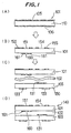
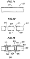
- According to the latter method, as shown in Fig. 62, the via-
holes laser beams 81 reflect on theinnerlayer conductor circuits - In the printed wiring board, however, a relatively shallow via-
hole 99a arrived at theinnerlayer conductor circuit 95 near to the outermost surface of the printed wiring board and a relatively deep via-hole 99b arrived at theinnerlayer conductor circuit 97 far away from the outermost surface are existent together as the via-hole as shown in Fig. 62. - As a result, when the holes are formed through the
laser beam 81, as shown in Fig. 63, there may be causeddamages 98 such as breakage, swell and the like in a central portion of theinnerlayer conductor circuit 95 arranged in the bottom of the shallow via-hole 99b though theinnerlayer conductor circuit 97 arranged in the bottom of the deep via-hole 99b is not damaged. - Once such damages are caused, when a metal plated film is formed on each surface of the
innerlayer conductor circuit 95 and via-hole 99a and between such a surface and an outer conductor circuit,pieces 98a of the innerlayer conductor circuit broken due to thedamage 98 remain in the via-hole 99a, so that the metal plated film may not be formed sufficiently. Such an insufficient metal plated film badly affects electric conduction between theinnerlayer conductor circuit 95 and theouter conductor circuit 94 and sometimes rejects the printed wiring board itself - The reason why the damage is caused in the
innerlayer conductor circuit 95 as mentioned above is due to the fact thatlaser beams 81 having an intensity required for the formation of the deep via-hole 99b are irradiated to not only the shallow via-hole 99a but also the deep via-hole 99b as shown in Fig. 62. - Therefore, it is also considered to irradiate a laser beam having an intensity in accordance with the depth of the via-hole to be formed. However, the number of via-holes formed in one printed wiring board is as many as, for example, 500∼10000, so that it is complicated to adjust the intensity of the laser beam every via-hole and also it is required to use an expensive control device for such an adjustment.
- Furthermore, a black oxide film is formed on the surfaces of the
innerlayer conductor circuits insulating layers - And also, the insulating layer made of the resin or the like is exposed in the via-hole, so that it is difficult to form the metal plated film. For this end, the joining property between he inner wall of the via-hole and the metal plated film is low and the peeling, dropping-out and the like of the metal plated film are caused, which have a fear of badly affecting the electric conduction of the via-hole.
- The formation of the metal plated film on the via-hole is carried out by flowing an electric plating solution into the via-hole, but as the inner diameter of the hole becomes small, the flowing of the electric plating solution is difficult to make the formation of the plated film ununiform, so that there is caused a fear that the electric conduction of the via-hole is insufficient.
- Further, it is attempted to provide the electric conduction by filling a solder in the via-hole instead of the metal plated film. In this case, the joining strength between the inner wall of the via-hole and the solder is low and there is a case that the solder is get out from the via-hole through an external pressure.
- Moreover, it is required to utilize the irradiation of the laser beam to the formation of holes other than the via-hole.
- In the light of the above problems, the invention is to provide a printed wiring board and a method of manufacturing the same which can form via-holes having a reliable electric conduction without causing damages of innerlayer conductor circuits through a laser beam and realize novel circuit formation through the laser beam.
- A first aspect of the invention lies in a method of manufacturing a printed wiring board comprising at least two insulating layers made of a synthetic resin, an innerlayer conductor circuit arranged between the insulating layers, and a blind via-hole formed from an outermost surface of the insulating layer toward the innerlayer conductor circuit, characterized in that an opening hole is previously formed in a central portion of the innerlayer conductor circuit located in a bottom portion of the blind via-hole, and a laser beam is irradiated from the outermost surface of the insulating layer to form the blind via-hole, and then a metal plated film is formed on the innerlayer conductor circuit and the surface of the blind via-hole.
- In the first aspect of the invention, it is most noticed that the opening hole is previously formed in the central portion of the innerlayer conductor circuit.
- In the first aspect of the invention, the blind via-hole ranging from the outermost surface of the printed wiring board to the innerlayer conductor circuit is formed by irradiating the laser beam toward a portion forming the blind via-hole.
- In this case, the insulating layer in the printed wiring board is vaporized and removed by a higher energy of the laser beam, whereby hole is gradually formed toward the inside of the printed wiring board. When the top of the laser beam arrives at the innerlayer conductor circuit the laser beam is reflected by the innerlayer conductor circuit made of the metal. At this time, the irradiation of the laser beam is stopped. Thus, the formation of the blind via-hole is terminated.
- It is important that the formation of many blind via-holes is carried out, for example, by successively and spottedly irradiating the laser beam every hole. On the other hand, the irradiation time and energy required for the formation of the hole differ between the shallow blind via-hole and the deep blind via-hole.
- However,the irradiation is conducted successively and continuously as mentioned above, so that all holes are formed under the same condition every the hole by setting the time and energy so as to surely form the deep blind via-hole.
- In the first aspect of the invention, the opening hole is formed in the innerlayer conductor circuit corresponding to the shallow blind via-hole.
- In the formation of the shallow blind via-hole, therefore, even the laser beam already arrives at the innerlayer conductor circuit to complete the formation of the via-hole, the laser beam is successively irradiated under the condition forming the deep blind via-hole. In this case, however, a central portion of the laser beam having a large energy is irradiated to the opening hole to pass therethrough.
- The laser beam passing through the opening hole is irradiated only to the insulating layer ahead the opening hole. Therefore, the insulating layer ahead the opening hole is somewhat pierced in the portion of the innerlayer circuit conductor, but the damage is not caused in the innerlayer conductor circuit itself.
- On the other hand, the irradiation of the laser beam is stopped at a time of reflecting on the innerlayer conductor circuit in the formation of the deep blind via-hole, so that the damage is not caused.
- And also, there is a method of simultaneously irradiating laser beams to all holes to be formed irrespectively of the shallow blind via-hole and deep blind via-hole. In this case, there are obtained the same function and effect as mentioned above (see the following embodiments).
- With respect to the thus obtained blind via-holes having different depths, the metal plated film is formed in the inside of each hole in the same manner as in the conventional technique. In this case, all of the innerlayer conductor circuits do not cause the damage through the laser beam as mentioned above, so that a state of forming the insufficient metal plated film as described in the conventional technique can be avoided and the metal plated film having an excellent electric conduction can be formed.
- As the insulating layer made of the synthetic resin in the first aspect of the invention, there are a synthetic resin alone, a resin substrate comprised of a synthetic resin and an inorganic filler, and a cloth substrate comprised of a synthetic resin and an inorganic cloth.
- As the synthetic resin, mention may be made of epoxy resin, phenolic resin, polyimide resin, polybutadiene resin, fluoride resin and the like. The insulating layer made of only such a synthetic resin may be formed between another insulating layers as a prepreg adhesion layer as shown in the following embodiment.
- As the inorganic filler added to the synthetic resin, mention may be made of glass short fibers, silica powder,mica powder, alumina, carbon and so on. The substrate made of a mixture of the synthetic resin and the inorganic filler is high in the strength as compared with the synthetic resin alone.
- And also, the cloth substrate is a substrate comprised of a woven or knitted cloth and a synthetic resin such as glass-epoxy substrate, glass-polyimide substrate and so on. As such a cloth substrate, there is a substrate formed by impregnating the cloth with the synthetic resin. As a material of the cloth, there are glass fiber cloth, carbon cloth, aramide cloth and so on. As the synthetic resin, use may be made of the above materials.
- The formation of the via-hole through the laser beam is carried out by irradiating the laser beam to a portion forming the blind via-hole. As the laser beam, it is preferable to use a carbon dioxide gas laser having a large energy and an excimer laser having no heat affection.
- The blind via-hole is formed up to a given innerlayer conductor circuit arranged at the inside of the printed wiring board. In the thus formed blind via-hole, the metal plated film is continuously formed from the innerlayer conductor circuit at the bottom of the via-hole through a wall face of the via-hole to an outer conductor circuit.
- When the innerlayer conductor circuit is provided on two or more stages in the printed wiring board and the blind via-hole is formed on each of the innerlayer conductor circuit, it is favorable to irradiate the laser beam at a state that the opening hole is formed in the innerlayer conductor circuit near to the outermost surface at a side of irradiating the laser beam, while the opening hole is not formed in the innerlayer conductor circuit far away from the outermost surface. Thus, there can be obtained the same function and effect as mentioned above.
- The opening hole formed in the innerlayer conductor circuit is preferable to be 30∼60% of a diameter of the blind via-hole. When the diameter of the opening hole is less than 30%, if a distance between the innerlayer conductor circuit having the opening hole and the deepest innerlayer conductor circuit having no opening hole is large, there is caused a fear that the innerlayer conductor circuit having the opening hole is damaged by the laser beam. On the other hand, when it exceeds 60%, there is caused a fear that the connection between copper plated film and the innerlayer conductor circuit is insufficient
- The metal plated film is favorable to be formed so as to cover the opening hole in the innerlayer conductor circuit. Thus, the bottom of the blind via-hole is completely covered with the metal plated film, so that there is caused no penetration of humidity into the blind via-hole.
- Moreover, the first aspect of the invention is applicable to printed wiring boards requiring high connection reliability such as memory module, multi-chip module, mother board, daughter board, plastic package and the like.
- A second aspect of the invention lies in a method of manufacturing a printed wiring board comprising at least two insulating layers made of a synthetic resin, an innerlayer conductor circuit arranged between the insulating layers, and a plurality of blind via-holes formed from an outermost surface toward the innerlayer conductor circuit and having different depths by successively irradiating a laser beam every a portion forming the blind via-hole, characterized in that a shallowest blind via-hole is formed as a standard hole by using a standard laser beam having an energy strength required for the formation of the standard hole, and the standard laser beam is irradiated plural times in the formation of the blind via-holes having deeper depths.
- In the second aspect of the invention, it is most noticed that the standard hole is formed by irradiating the standard laser beam, while the blind via-holes having a depth deeper than the standard hole are formed by irradiating the standard laser beam plural times.
- The function and effect of the second aspect of the invention will be described below.
- In the second aspect of the invention, the blind via-hole ranging from the outermost surface of the printed wiring board to the innerlayer conductor circuit is formed by irradiating the laser beam toward a portion forming the blind via-hole.
- In this case, the insulating layer in the printed wiring board is vaporized and removed by a higher energy of the laser beam, whereby hole is gradually formed toward the inside of the printed wiring board. When the top of the laser beam arrives at the innerlayer conductor circuit, the laser beam is reflected by the innerlayer conductor circuit made of the metal. At this time, the irradiation of the laser beam is stopped. Thus, the formation of the blind via-hole is terminated.
- And also, the formation of many blind via-holes is carried out, for example, by successively and spottedly irradiating the laser beam every hole. In this case, the irradiation time and energy required for the formation of the hole differ between the shallow blind via-hole and the deep blind via-hole.
- In the second aspect of the invention, therefore, the standard laser beam having an energy strength required for the formation of a shallowest blind via-hole as a standard hole is used and the formation of the standard hole is conducted by irradiating the standard laser beam at a time. On the other hand, the blind via-holes having a depth deeper than the standard hole are formed by irradiating the standard laser beam plural times.
- According to the second aspect of the invention, therefore, many blind via-holes are divided into the standard holes and the other blind via-holes, and the irradiation number of the standard laser beam may be determined in accordance therewith. And also, the blind via-holes other than the standard hole have several kinds of depths. The depth of each blind via-hole can previously be known in the planning of the printed wiring board.
- On the other hand, an oscillator for the laser beam irradiates the standard laser beam every a case that the oscillator is moved to a coordinate point indicating, for example, a position of each blind via-hole. And also, the movement and stop to the coordinate point are carried out by N/C control by means of a coordinate control device for the positioning.
- When the irradiation number of the standard laser beam required every the blind via-hole is set, for example, in the laser beam oscillator positioned by the coordinate control device, therefore, the energy strength required every the blind via-hole can be irradiated.
- As a result, the time required for the formation of many blind via-holes is shortened and the cost can be reduced. And also, it is enough to control whether or not the irradiation is required plural times, so that the cost of the device can be reduced.
- According to the second aspect of the invention, therefore, many blind via-holes having different depths can easily be formed only by adjusting the irradiation number of the standard laser beam.
- Moreover, the depth of the blind via-hole is a depth ranging from the outermost surface of the printed wiring board to the innerlayer conductor circuit (including a lower circuit at a bottom surface), and each depth differs in accordance with a distance between the innerlayer conductor circuits. And also, the distance is determined by a thickness of the insulating layer between the innerlayer conductor circuits. Therefore, the depth of the blind via-hole other than the standard hole becomes generally near to an integer times a depth of the standard hole. As a result, the blind via-holes other than the standard hole can be formed by irradiating the standard laser beam plural times.
- As the insulating layer made of the synthetic resin in the second aspect of the invention, there are a synthetic resin alone, a resin substrate comprised of a synthetic resin and an inorganic filler, and a cloth substrate comprised of a synthetic resin and an inorganic cloth.
- As the synthetic resin, mention may be made of epoxy resin, phenolic resin, polyimide resin, polybutadiene resin, fluoride resin and the like. The insulating layer made of only such a synthetic resin may be formed between another insulating layers as a prepreg adhesion layer.
- As the laser beam, it is preferable to use a carbon dioxide gas laser having a large energy and an excimer laser having no heat affection.
- For example, the energy strength of the standard laser beam can experimentally be determined by frequency, power (W) and irradiation time of the laser beam.
- Moreover, the blind via-hole is formed up to a given innerlayer conductor circuit. In the thus formed blind via-hole, a metal plated film is continuously formed from the innerlayer conductor circuit at the bottom of the via-hole through the inner wall of the via-hole to an outer conductor circuit (see Fig. 10).
- Furthermore, it is favorable that the standard laser beam is irradiated one time to the formation of all blind via-holes and thereafter the standard laser beam is irradiated only to the blind via-holes having a depth deeper than the standard hole at irradiation number required for the formation of these via-holes.
- In this way, there can be obtained an effect of forming holes having various depths at a uniform state in the same cycle.
- The standard laser beam is irradiated so as to successively form adjacent blind via-holes. In this case, it is favorable that one irradiation is conducted in the formation of the standard hole and the irradiation for the formation of the blind via-holes having a depth deeper than the standard hole is conducted at number required for such a via-hole each time.
- Thus, movement not requiring for the formation such as movement of a table or the like can be controlled to a minimum level, so that a total formation time can be shortened.
- Moreover, the second aspect of the invention is applicable to printed wiring boards requiring high connection reliability such as memory module, multi-chip module, mother board, daughter board, plastic package and the like.
- A third aspect of the invention lies in a method of manufacturing a printed wiring board by forming an innerlayer conductor circuit on a surface of an innerlayer substrate, forming a black oxide film on a surface of the innerlayer conductor circuit, forming a second conductor circuit onto the innerlayer substrate through an insulating layer, irradiating a laser beam to form a via-hole ranging from an outer most surface of the insulating layer to the innerlayer conductor circuit, and then forming a metal plated film onto an inner wall face of the via-hole, characterized in that a portion of the innerlayer conductor circuit irradiated by the laser beam is an exposed portion having no black oxide film.
- The formation of hole through the laser beam is carried out by irradiating the laser beam to a portion forming the via-hole. As the laser beam, it is favorable to use a carbon dioxide gas laser having a large energy and an excimer laser having no heat affection.
- And also, the formation of the via-hole through the laser beam is conducted by vaporizing and removing the insulating layer by a higher energy of the laser beam to successively form a hole toward the inside of the printed wiring board. When the top of the laser beam arrives at the innerlayer conductor circuit, the laser beam is reflected by the innerlayer conductor circuit made of the metal. At this time, the irradiation of the laser beam is stopped.
- The function of the third aspect of the invention will be described.
- In the method according to the third aspect of the invention, the portion irradiated by the laser beam is an exposed portion of the innerlayer conductor circuit having no black oxide film.
- Therefore, the laser beam is reflected by the innerlayer conductor circuit made of the metal and hardly absorbed by the innerlayer conductor circuit. As a result, it can be prevented to abnormally heat the innerlayer conductor circuit, so that there is not caused the damage of the innerlayer conductor circuit through heat.
- In the third aspect of the invention, therefore, the via-hole can be formed by using the laser beam without damaging the innerlayer conductor circuit. And also, the via-hole is formed by the laser beam, so that via-holes having a smaller diameter can be obtained and it is easy to manufacture a printed wiring board having high density and accuracy.
- As mentioned above, according to the third aspect of the invention, there can be provided a method of manufacturing a multilayer printed wiring board without causing the damage of the innerlayer conductor circuit in the formation of the via-hole through the laser beam.
- Furthermore, the printed wiring board obtained in the third aspect of the invention can be used in memory module, multi-chip module, mother board, daughter board, plastic package and the like which require a high connection reliability.
- The exposed portion is preferable to be formed by forming the black oxide film on the innerlayer conductor circuit and thereafter etching the black oxide film. Thus, the black oxide film can easily be formed at arbitrary positions.
- Alternatively, the exposed portion is preferable to be formed by partly masking the innerlayer conductor circuit so as not to form the black oxide film in the formation of the black oxide film on the innerlayer conductor circuit.
- In this way, the exposed portion can easily be formed in the formation of the black oxide film.
- The insulating layer and the second conductor circuit are favorable to be formed at two or more sets. Thus, there can easily be obtained a printed wiring board of high density wiring.
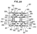
- Moreover, when the insulating layer and the second conductor circuit are two or more sets, a set of certain insulating layer and second conductor circuit formed thereon is provided on its surface with another set of different insulating layer and second conductor circuit formed thereon (see Fig. 20). That is, the second conductor circuit is formed on the insulating layer, so that they are used as one set for the formation of the multi-layer.
- In this case, a via-hole ranging from an outermost surface of an outermost insulating layer to a surface of either second conductor circuit may be formed (see Fig. 20).
- Furthermore, it is favorable that the black oxide film is also formed on the surface of the second conductor circuit likewise the innerlayer conductor circuit and the portion irradiated by the laser beam for the formation of the via-hole is an exposed portion having no black oxide film (see the following embodiment 3).
- Moreover, the printed wiring board obtained by the above method is, for example, a printed wiring board comprising an insulating layer, an innerlayer conductor circuit arranged adjacent to the insulating layer and provided on its surface with a black oxide film and a via-hole extending from an outermost surface of the insulating layer to the innerlayer conductor circuit, characterized in that an exposed portion having no black oxide film is formed on the innerlayer conductor circuit in a position corresponding to the bottom of the via-hole.
- In such a printed wiring board, the black oxide film is not existent on the portion of the innerlayer conductor circuit corresponding to the bottom of the via-hole, so that the innerlayer conductor circuit is exposed at this portion. The laser beam is hardly absorbed on this portion.
- Therefore, when the laser beam is irradiated to the insulating layer for forming the via-hole in the insulating layer, it can be prevented to abnormally heat the innerlayer conductor circuit and also it can be prevented to cause the damage due to fusion of the innerlayer conductor circuit or the like.
- As mentioned above, according to the third aspect of the invention, there can be provided the multilayer printed wiring board causing no damage in the innerlayer conductor circuit in the formation of the via-hole through the laser beam.
- A fourth aspect of the invention lies in a printed wiring board comprising two or more insulating layers located on an innerlayer conductor circuit, a via-hole extending from an outermost surface of the insulating layer through the two or more insulating layers to the innerlayer conductor circuit, and an inner metal plated film formed in the via-hole and electrically connecting the innerlayer conductor circuit to an outer conductor circuit formed on the outermost surface, characterized in that an annular middle land having an opening hole is arranged so as to protrude into the inside of the via-hole, and the via-hole is a stepped via-hole consisting of an outer via-hole segment located outside the annular middle land and an inner via-hole segment located at the side of the innerlayer conductor circuit and having a diameter smaller than that of the outer via-hole segment and a stepped portion located at the annular middle land, and the inner metal plated film is a stepped plated film formed along inner wall faces of the outer via-hole segment and the inner via-hole segment.
- The function of the fourth aspect of the invention will be described below.
- In the printed wiring board according to the fourth aspect of the invention is arranged the annular middle land having an opening hole so as to protrude into the inside of the via-hole. And also, the via-hole is a stepped via-hole having a stepped portion on the annular middle land. Furthermore, the inner metal plated film is a stepped plated film formed along the inner wall faces of the outer via-hole segment and the inner via-hole segment.
- The annular middle land is exposed in the stepped portion of the via-hole. Such an exposed portion is a ring having an outer diameter equal to the diameter of the outer via-hole segment and an inner diameter equal to the diameter of the inner via-hole segment. This portion contacts with the inner metal plated film forming the stepped plated film (see Fig. 27).
- The inner metal plated film hardly joins to the exposed portion of the insulating layer in the via-hole, but can strongly join to the annular middle land. Therefore, the inner metal plated film is joined to the exposed portion of the annular middle land, whereby it can strongly be joined to the inside of the via-hole.
- And also, the side face of the opening hole in the annular middle land is exposed to the via-hole, so that the inner metal plated film can also be joined to this portion.
- Therefore, the peeling and dropping of the inner metal plated film can be prevented.
- Now, a boundary conductor circuit as mentioned later may be arranged in a boundary portion. However, when the via-hole is formed in a portion having no boundary conductor circuit, a thickness of an opening peripheral edge of the via-hole becomes thinner by a thickness of the boundary conductor circuit as compared with a place having the boundary conductor circuit arranged in the boundary portion. As a result, a depression corresponding to the thickness of the boundary conductor circuit is formed in the opening peripheral edge of the via-hole.
- When the annular middle land is arranged, the thickness of the annular middle land thickens the thickness of the opening peripheral edge of the via-hole, so that the occurrence of the depression in the opening peripheral edge of the via-hole can be prevented.
- As mentioned above, according to the fourth aspect of the invention, there can be provided the printed wiring board wherein the inner metal plated film is strongly joined to the inside of the via-hole.
- It is favorable that the annular middle land is a dummy land not connected to the boundary conductor circuit arranged in the boundary portion facing tow or more insulating layers to each other.
- Thus, when many insulating layers are laminated, even if via-holes are formed portions of these insulating layers having no boundary conductor circuit, the occurrence of the depression in the opening peripheral edge of the via-hole can be prevented.
- It is favorable that the annular middle land is an electrically conductive land connecting to the boundary conductor circuit arranged in the boundary portion facing two or more insulating layers to each other.
- In this case, three or more conductor layers can be connected to each other through one via-hole. Therefore, the wiring area of the via-hole and land is reduced, so that it is possible to make a high densification.
- The annular middle land is preferable to be made of a metal such as copper, nickel or the like.
- As the method of manufacturing the above printed wiring board, there is, for example, a method of manufacturing a printed wiring board by arranging two or more insulating layers on an innerlayer conductor circuit, forming a via-hole so as to extend from an outermost surface of the insulating layer through the two or more insulating layers to the innerlayer conductor circuit, forming an inner metal plated film in the via-hole to electrically conduct the innerlayer conductor circuit to an outer conductor circuit arranged on the outermost surface, arranging an annular middle land having an opening hole so as to protrude into the inside of the via-hole, wherein the via-hole is a stepped via-hole consisting of an outer via-hole segment located outside the annular middle land and an inner via-hole segment located at the side of the innerlayer conductor circuit and having a diameter smaller than that of the outer via-hole segment and a stepped portion located at the annular middle land, and the inner metal plated film is a stepped plated film formed along inner wall faces of the outer via-hole segment and the inner via-hole segment, characterized in that the via-hole is formed by irradiating a laser beam from the outermost surface toward the innerlayer conductor circuit in which the laser beam is arrived to the innerlayer conductor circuit through the opening hole of the annular middle land and irradiated to a range required for forming the diameter of the outer via-hole segment, and the metal plated film is formed after the formation of the via-hole.
- According to this manufacturing method, the printed wiring board wherein the inner metal plated film is strongly joined to the inside of the via-hole can be provided likewise the fourth aspect of the invention.
- Since the via-hole is formed by the irradiation of the laser beam, via-holes having a very fine diameter of not more than 300 µm can easily be obtained.
- As mentioned above, according to this method, there can easily be manufactured a printed wiring board having fine-diameter via-holes in which the inner metal plated film is strongly joined to the inside of the via-hole.
- The formation of the via-hole through the laser beam is carried out by irradiating the laser beam to a portion forming the via-hole. As the laser beam, it is favorable to use a carbon dioxide gas laser having a large energy and an excimer laser having no heat affection.
- And also, in the formation of the via-hole by the irradiation of the laser beam, the insulating layers are vaporized and removed by a high energy to successively form a hole toward the inside of the printed wiring board.
- In this case, the laser beam forming the neighborhood of the outer diameter of the via-hole is reflected on the annular middle land. Therefore, the insulating layer existing beneath the annular middle land remains as it is.
- Furthermore, the laser beam forming a central portion of the via-hole passes through the opening hole of the annular middle land to vaporize and remove a further lower insulating layer. Thereafter, when the laser beam arrives at the innerlayer conductor circuit, it is reflected by the innerlayer conductor circuit made of the metal. Therefore, the irradiation of the laser beam stops at this time.
- Thus, the via-hole formed by the laser beam is large in the outer diameter at a position above the annular middle land and small in the outer diameter located beneath the annular middle land.
- That is, the stepped via-hole having a stepped portion can be formed.
- The annular middle land is preferable to be a dummy land not connecting to the boundary conductor circuit arranged in the boundary portion facing the two or more insulating layers to each other.
- The annular middle land is preferable to be an electrically conductive land connecting to the boundary conductor circuit arranged in the boundary portion facing the two or more insulating layers to each other.
- In any case, the same function and effect as mentioned above can be obtained.
- A fifth aspect of the invention lies in a printed wiring board comprising two or more insulating layers on an innerlayer conductor circuit, a via-hole extending from an outermost surface of the insulating layer through the two or more insulating layers to the innerlayer conductor circuit and an inner metal plated film formed in the via-hole so as to electrically connect the innerlayer conductor circuit to an outer conductor circuit arranged on the outermost surface, characterized in that an annular dummy land for reinforcement having an opening hole around the via-hole is arranged in a boundary portion facing the two or more insulating layers to each other and is joined to the inner metal plated film.
- In the printed wiring board, an innerlayer conductor circuit may be arranged in the boundary portion, but the annular dummy land is separately arranged so as not to connect to such an innerlayer conductor circuit and is a reinforcing land. The annular dummy land is favorable to be made of a metal such as copper nickel or the like.
- The function of the fifth aspect of the invention will be described below.
- In the printed wiring board according to the fifth aspect of the invention, the annular reinforcing dummy land is arranged around the via-hole and is joined to the inner metal plated film in the via-hole.
- The inner metal plated film hardly joins to an exposed portion of the insulating layer in the via-hole, but strongly joins to the side face of the annular dummy land. Therefore, the inner metal plated film is strongly joined to the inside of the via-hole.
- As a result, the peeling and dropping-out of the inner metal plated film can be prevented.
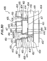
- Now, the innerlayer conductor circuit may be arranged in the boundary portion, but when the via-hole is formed in a portion having no innerlayer conductor circuit, an opening peripheral edge of the via-hole becomes thin by a thickness of the innerlayer conductor circuit as compared with a place having the innerlayer conductor circuit in the boundary portion. For this end, a depression corresponding to the thickness of the innerlayer conductor circuit is formed in the opening peripheral edge of the via-hole. This is particularly liable to be caused in the via-hole formed by passing through four or more insulating layers (see Fig. 33). The occurrence of the depression in the opening peripheral edge of the via-hole can be prevented by arranging the annular dummy land.
- As mentioned above, according to the fifth aspect of the invention, there can be provided the printed wiring board in which the inner metal plated film is strongly joined to the inside of the via-hole.
- And also, the printed wiring board obtained in the fifth aspect of the invention can be used in, for example, memory module, multi-chip module, mother board, daughter board, plastic package or the like which highly requires the connection reliability.
- The annular dummy land is favorable to have an outer diameter larger than the diameter of the via-hole and include an opening hole having a diameter equal to the diameter of the via-hole.
- Thus, the annular dummy land can more stably be arranged and also the reinforcing effect can be more enhanced.
- As the method of manufacturing the above printed wiring board, there is a method of manufacturing a printed wiring board comprising two or more insulating layers on an innerlayer conductor circuit, a via-hole extending from an outermost surface of the insulating layer through the two or more insulating layers to the innerlayer conductor circuit and an inner metal plated film formed in the via-hole so as to electrically connect the innerlayer conductor circuit to an outer conductor circuit arranged on the outermost surface, wherein an annular dummy land for reinforcement having an opening hole around the via-hole is arranged in a boundary portion facing the two or more insulating layers to each other and is joined to the inner metal plated film, characterized in that the via-hole is formed by irradiating a laser beam from the outermost surface toward the innerlayer conductor circuit in which the laser beam is arrived to the innerlayer conductor circuit through the opening hole of the annular dummy land, and thereafter the inner metal plated film is formed.
- According to this method, a printed wiring board wherein the inner metal plated film is strongly joined to the inside of the via-hole can be obtained likewise the above printed wiring board.
- Since the via-hole is formed by the irradiation of the laser beam, via-holes having a very fine diameter of not more than 300 µm can easily be obtained.
- As mentioned above, according to this method, there can easily be manufactured a printed wiring board having fine-diameter via-holes in which the inner metal plated film is strongly joined to the inside of the via-hole.
- The formation of the via-hole through the laser beam is carried out by irradiating the laser beam to a portion forming the via-hole. As the laser beam, it is favorable to use a carbon dioxide gas laser having a large energy and an excimer laser having no heat affection.
- And also, in the formation of the via-hole by the irradiation of the laser beam, the insulating layers are vaporized and removed by a high energy to successively form a hole toward the inside of the printed wiring board. When the laser beam arrives at the innerlayer conductor circuit, it is reflected by the innerlayer conductor circuit made of the metal. Therefore, the irradiation of the laser beam stops at this time.
- The annular dummy land is favorable to have an outer diameter larger than the diameter of the via-hole and include an opening hole having a diameter equal to the diameter of the via-hole.
- Thus, the annular dummy land can more stably be arranged and also the reinforcing effect can be more enhanced likewise the above case.
- A sixth aspect of the invention lies in a printed wiring board comprising an insulating layer, an upper conductor circuit arranged on an upper surface of the insulating layer, a lower conductor circuit arranged on a lower surface thereof, a blind via-hole passing through the insulating layer between the upper conductor circuit and the lower conductor circuit and bottomed at the lower conductor circuit and a via-plated layer formed on an inner wall face of the blind via-hole so as to electrically connect the upper conductor circuit to the lower conductor circuit, characterized in that a flowing hole of a plating solution having a diameter smaller than the blind via-hole is formed in the lower conductor circuit constituting the bottom of the blind via-hole.
- The diameter of the flowing hole of the plating solution differs in accordance with the diameter of the blind via-hole, but when the diameter of the blind via-hole is 0.1∼0.3 mm, the diameter of the flowing hole of the plating solution is preferable to be 0.01∼0.1 mm.
- Thus, the uniform via-plated layer can be obtained.
- Moreover, when the diameter of the flowing hole is less than 0.01 mm, it is feared that the object of flowing the plating solution can not be attained. While, when it exceeds 0.1 mm, the hole is not closed with the plated film and it is feared to cause a problem that a leakage of a solder is created in the filling of the solder.
- The function of the sixth aspect of the invention will be described below.
- In the printed wiring board according to the sixth aspect of the invention, the flowing hole of the plating solution having a diameter smaller than the blind via-hole is formed in the lower conductor circuit constituting the bottom of the blind via-hole.
- In the formation of the via-plated layer, the plating solution can be flowed through the flowing hole into inside and outside of the blind via-hole. For this end, the plating solution sufficiently containing a plating component always contacts with the inner wall face of the blind via-hole, so that the uniform via-plated layer can be obtained without causing a spotted state.
- Therefore, there can be obtained the printed wiring board having an excellent electric conduction between the upper conductor circuit and the lower conductor circuit or an excellent connection reliability therebetween.
- As mentioned above, according to the sixth aspect of the invention, there can be provided a printed wiring board wherein the via-plated layer is uniformly formed on the blind via-hole without causing the spotted state.
- The printed wiring board obtained in the sixth aspect of the invention can be used in, for example, memory module, multi-chip module, mother board, daughter board, plastic package or the like which highly requires the connection reliability.
- Of course, the sixth aspect of the invention is applicable to not only the printed wiring board having a single insulating layer but also the printed wiring board having plural insulating layers.
- It is preferable that the flowing hole of plating solution is closed with the via-plated layer. Thus, a quantity of the solder can be uniformed in the filling of the solder.
- It is favorable that the diameter of the flowing hole of plating solution is 10∼40% of the diameter of the blind via-hole. Thus, the flowing of the plating solution can sufficiently be carried out. On the other hand, when the diameter of the flowing hole is less than 10% of the diameter of the blind via-hole, there is a fear that the object of flowing the plating solution can not be attained. While, when it is more than 40%, there is a fear that the closing of the hole by plating is insufficient.
- As the method of manufacturing the above printed wiring board, there is a method of manufacturing a printed wiring board comprising an insulating layer, an upper conductor circuit arranged on an upper surface of the insulating layer, a lower conductor circuit arranged on a lower surface thereof, a blind via-hole passing trough the insulating layer between the upper conductor circuit and the lower conductor circuit and bottomed at the lower conductor circuit and a via-plated layer formed on an inner wall face of the blind via-hole so as to electrically connect the upper conductor circuit to the lower conductor circuit, wherein a flowing hole of a plating solution having a diameter smaller than the blind via-hole is formed in the lower conductor circuit constituting the bottom of the blind via-hole, characterized in that the blind via-hole is formed by irradiating a laser beam from the upper surface of the insulating layer toward the lower conductor circuit, and the flowing hole of the plating solution is formed in the lower conductor circuit through the laser beam in the formation of the blind via-hole, and a chemical plating solution is flowed in the blind via-hole and the flowing hole of the plating solution to form a chemical plated layer in the blind via-hole, and thereafter an electroplating is carried out by flowing an electroplating solution to form the via-plated layer.
- In this manufacturing method, the electroplating is carried out by utilizing the flowing hole of the plating solution formed in the lower conductor circuit and flowing the electroplating solution to form the via-plated layer. In this case, the electroplating solution can sufficiently be come and gone to the outside and inside of the blind via-hole through the flowing hole of the plating solution. Thus, the uniform via-plated layer can be obtained without causing the spotted state.
- Since the via-hole is formed by the laser beam, via-holes having a smaller diameter can be obtained, so that t is easy to manufacture a printed wiring board having high density and accuracy.
- Moreover, the formation of via-hole through the maser beam is carried out by irradiating the laser beam to a portion forming the via-hole. As the laser beam, it is favorable to use a carbon dioxide gas laser having a large energy and an excimer laser having no heat affection.
- In the formation of the via-hole by the irradiation of the laser beam, the insulating layer is vaporized and removed by a high energy to successively form the via-hole toward the inside of the printed wiring board. When the top of the laser beam arrives at the lower conductor circuit, it is reflected on the lower conductor circuit made of a metal. Therefore, the irradiation of the laser beam stops at this time.
- And also, the energy of the laser beam is high in the central portion and low in the peripheral edge portion. Therefore, the flowing hole of the plating solution can easily be formed in the central portion of the lower conductor circuit constituting the bottom of the blind via-hole by using the laser beam.
- It is favorable that an exposed portion of the insulating layer for the formation of the flowing hole of the plating solution (i.e. a portion having no innerlayer conductor circuit) is previously formed in the innerlayer conductor circuit. The laser beam is reflected because the lower conductor circuit is made of a metal such as copper foil or the like. By forming the exposed portion, the insulating layer located above the exposed portion is vaporized and removed,whereby the flowing hole of the plating solution can be obtained.
- A seventh aspect of the invention lies in a method of manufacturing a printed wiring board comprising a step of forming an upper pattern on an upper surface of an insulating substrate in a peripheral edge of a portion for the formation of an electric conduction hole, a step of forming a lower pattern closing the portion for the formation of the electric conduction hole on a lower surface of the insulating substrate, a step of forming the electric conduction hole in the insulating substrate, and a step of a metal plated film on an inner wall face of the electric conduction hole by a chemical plating treatment and an electroplating treatment, characterized in that the electroplating treatment is carried out by applying a current having a current density of 0.8∼1.4 A/dm2 to a chemical plated film covering the inner wall face of the electric conduction hole at a state of immersing the insulating substrate in an electroplating bath.
- The function and effect of the seventh aspect of the invention will be described below.
- In the seventh aspect of the invention, the current density of the current applied to the chemical plated film is made smaller than that of the conventional technique as mentioned above. For this end, a thick plated film can be formed in the inner wall face of the electric conduction hole. Therefore, the mechanical strength of the metal plated film becomes high and the electric connection reliability of the electric conduction hole is improved.
- And also, the metal plated film having a sufficient thickness can be formed even on the inner wall face of the electric conduction hole having a smaller diameter, so that the high density packaging of the electric conduction hole can be realized.
- Moreover, the step of forming the upper pattern, the step of forming the lower pattern and the step of forming the electric conduction hole may be conducted either way and are not in order
- The metal plated film is preferable to be copper. In this case, the metal plated film having a good ductility and a small electric resistance can be formed.
- The electroplating treatment is favorable to be carried out two or more times. Thus, the metal plated film having a thicker thickness can be formed in a short time. And also, the thickness of the metal plated film can be uniformed. On the other hand, when the electroplating treatment is conducted only one time, there is a case that a long time is taken in the formation of the thick metal plated film.
- The upper pattern and lower pattern mean any electric conducting patterns formable on the surface of the insulating substrate such as wiring circuit, pad, terminal, land and the like, which may be formed, for example, by etching of a metal foil, a metal plating or the like.
- As the insulating substrate, there are synthetic resin alone, prepreg and the like. As the synthetic resin, there are epoxy resin, phenolic resin, polyimide resin, polybutadiene resin, fluorine resin and so on.
- The printed wiring board is composed of a single insulating substrate or of a laminate of two or more insulating substrates. In case of the laminate of two or more insulating substrates, the electric conduction hole may pass through all insulating substrates or may pass through a part of the insulating substrates.
- The above printed wiring board can be used in, for example, memory module, multi-chip module, mother board, daughter board, plastic package or the like.
- As the formation of the electric conduction hole, there are, for example, a method of irradiating a laser beam to a hole forming portion of the insulating layer, a method of chemically melting a hole forming portion of the insulating layer and the like.
- An eighth aspect of the invention lies in a printed wiring board comprising an insulating substrate, a conductor pattern formed on a surface of the insulating substrate, a solder filling hole passing through the insulating substrate and arriving at an upper surface of the conductor pattern and a solder filled in the solder filling hole, characterized in that the insulating substrate includes fibers therein, and end portions of the fibers protrude from a wall face of the solder filling hole and encroach into the solder.
- The function and effect of the eighth aspect of the invention will be described below.
- In the eight aspect of the invention, the end portions of the fibers included in the insulating substrate protrude from the wall face of the solder filling hole. These end portions of the fibers encroach into the solder filled in the solder filling hole. Therefore, the solder is strongly bonded to the solder filling hole. As a result, even when the printed wiring board is subjected to dynamic action from exterior, the solder never gets out of the solder filling hole.
- Since the end portions of the fibers protruded from the wall face of the solder filling hole encroach into the solder, even when the insulating substrate is a thin sheet of about 0.05-0.20 mm and a bonding area between the solder and the solder filling hole is small, the solder never gets out of the solder filling hole. In the protrusion of the end portions of the fibers from the wall face of the solder filling hole, there is, for example, a method of conducting the formation of the solder filling hole through a laser beam.
- The fiber is preferable to be one or more of glass fiber, resin fiber and ceramic fiber. Thus, the encroaching force of the fiber into the inside of the solder is increased and the bonding strength between the solder and the solder filling hole is more increased.
- The fibers are included in the insulating substrate at a state of, for example, felt or cloth.
- As the method of producing the above printed wiring board, there is a method of a printed wiring board by filling a solder into an inside of a solder filling hole, characterized in that a conductor pattern is first formed on a surface of an insulating substrate including fibers, and then a laser beam is irradiated to a portion of the insulating substrate not covered with the conductor pattern toward the conductor pattern to form a solder filling hole at a state of protruding end portions of the fibers included in the inside of the insulating substrate from a wall face of the solder filling hole, and thereafter a solder is filled into the inside of the solder filling hole.
- In the method of the eighth aspect, the solder filling hole is formed by the irradiation of the laser beam, whereby the end portions of the fibers are left in the wall face of the solder filling hole. Therefore, the end portions of the fibers can easily be protruded from the wall face of the solder filling hole.
- And also, the laser beam can form the solder filling hole in only the insulating substrate, in which the conductor pattern covering an opening portion of the solder filling hole can be left as it is. For this end, the production step can be simplified by forming conductor patterns on front and back surfaces of the insulating substrate before the formation of the solder filling hole.
- The fiber is preferable to be one or more of glass fiber, resin fiber and ceramic fiber. Thus, the encroaching force of the fiber into the inside of the solder is increased and the bonding strength between the solder and the solder filling hole is more increased.
- The fibers are included in the insulating substrate at a state of, for example, felt or cloth.
- A ninth aspect of the invention lies in a printed wiring board comprising at least two insulating layers, an innerlayer conductor circuit between the insulating layers, a blind via-hole formed from an outermost surface toward the innerlayer conductor circuit, and a solder filled in the inside of the blind via-hole, characterized in that the blind via-hole has an uneven form at a section of its wall face.
- The function of the ninth aspect of the invention will be described below.
- In the printed wiring board according to the ninth aspect of the invention, the wall face of the blind via-hole has a section of uneven form.
- Therefore, the solder filled in the blind via-hole comes into the unevenness and is fixed thereto. As a result, the solder can provide a high bonding strength to the blind via-hole.
- The printed wiring board obtained in the ninth aspect of the invention can be used in, for example, memory module, multi-chip module, mother board, daughter board, plastic package or the like which highly requires the connection reliability.
- As the above uneven form, there are preferably a concave form widening in a lateral direction of the blind via-hole, a convex form protruding inward in the blind via-hole, and a wavy form (see Fig. 52, Fig. 54, Fig. 55 as mentioned later).
- In this way, the filled solder can surely be bonded to the inside of the blind via-hole.
- It is favorable that the solder filled in the blind via-hole is connected to another PC board through a solder ball.
- Thus, the electric conduction between the PC board and the blind via-hole can surely be held.
- Moreover, the PC board includes various boards provided with printed circuits. Concretely, there are mentioned mother board, daughter board, memory module, multi-chip module, card module and the like for various apparatuses.
- As the method of producing the above printed wiring board, there is a method of producing a printed wiring board, which comprises at least two insulating layers, an innerlayer conductor circuit between the insulating layers, a blind via-hole formed from an outermost surface toward the innerlayer conductor circuit and having an uneven form at a section of its wall face, and a solder filled in the inside of the blind via-hole, characterized in that the blind via-hole is formed by irradiating a laser beam, and thereafter molten solder is flowed into the blind via-hole.
- According to the above method, there can be produced the printed wiring board in which the section of the wall face of the blind via-hole is uneven form.
- Therefore, the solder filled in the blind via-hole can come into the unevenness. As a result, the solder can provide a high bonding strength to the blind via-hole.
- And also, the blind via-hole is formed by the irradiation of the laser beam, so that a very fine size of not more than 300 µm can be obtained.
- The formation of the blind via-hole trough the laser beam is carried out by irradiating laser beam to a portion forming the blind via-hole. As the laser beam, it is favorable to use a carbon dioxide gas laser having a large energy and an excimer laser having no heat affection.
- In the formation of the blind via-hole by the irradiation of the laser beam, the insulating layer is vaporized and removed by a high energy to successively form the via-hole toward the inside of the printed wiring board. When the top of the laser beam arrives at the innerlayer conductor circuit the laser beam is reflected on the innerlayer conductor circuit made of a metal. Therefore, the irradiation of the laser beam stops at this time.
- Moreover, it is favorable that the insulating substrate is comprised of a prepreg obtained by impregnating a resin into a substrate of glass cloth or the like because the blind via-hole having a section of irregular form can be obtained only by the irradiation of the laser beam.
- This is due to the fact that when the insulating substrate is vaporized and removed by the laser beam, the resin portion is removed before the substrate portion.
- Next, a tenth aspect of the invention is a method of forming a mounting recess portion by utilizing a technique of forming holes through the irradiation of the laser beam.
- That is, the tenth aspect of the invention lies in a method of producing a printed wiring board comprising a mounting recess portion for mounting an electronic part, a conductor pattern, and a heat-sink plate arranged at the bottom of the mounting recess portion, characterized in that a conductor pattern is formed on an insulating substrate;
- a heat-sink plate is adhered to a lower face of a portion of the insulating substrate forming the mounting recess portion; and
- a laser beam is irradiated to an upper face of the portion forming the mounting recess portion to form a mounting recess portion.
-
- The function and effect of the tenth aspect of the invention will be described below.
- In the tenth aspect of the invention, as shown in Fig. 56, after the portion of the insulating substrate forming the mounting recess portion is covered with the heat-sink plate, the mounting recess portion is formed by the irradiation of the laser beam. Therefore, an opening portion having a desired size can easily be obtained.
- In the tenth aspect of the invention, the laser beam is irradiated toward the portion forming the mounting recess portion to form the mounting recess portion ranging from the surface of the printed wiring board to the heat-sink plate adhered to the opposite side thereof.
- In this case, the portion of the insulating substrate forming the mounting recess portion is vaporized and removed by a high energy of the laser beam to successively form a hole toward the inside of the insulating substrate. When the top of the laser beam arrives at the heat-sink plate, the laser beam is reflected on the heat-sink plate. Therefore, the irradiation of the laser beam stops at this time. Thus, there can be formed the mounting recess portion of non-passing type in which one opening portion is covered with the heat-sink plate.
- Even when the insulating substrate is thin, the mounting recess portion can be formed without giving damage to the insulating substrate.
- Further, the bottom of the mounting recess portion is a surface of the heat-sink plate. Therefore, an electronic part is mounted onto the surface of the heat-sink plate in the inside of the mounting recess portion. As a result, the mounting recess portion having an excellent heat dissipation property can be formed.
- Even in case of forming the mounting recess portion passing through a plurality of insulating substrates, it is not required to form a through-hole for the formation of the mounting recess portion every the insulating substrate as in the conventional technique. Furthermore, the positioning of the insulating substrates for connecting the through-holes to each other is useless. Therefore, according to the tenth aspect of the invention, the mounting recess portion can be formed easily and accurately.
- It is preferable to be a method of producing a printed wiring board in which the insulating substrate is comprised by laminating two or more insulating layers and a conductor pattern is formed in the inside of the insulating substrate. Thus, a high density wiring of the printed wiring board can be realized.
- The thickness of the heat-sink plate is preferable to be 0.01-2 mm. In this case, a high strength is obtained at the bottom of the mounting recess portion and also the working of the heat-sink plate becomes easy. However, when it is less than 0.01 mm, the strength at the bottom of the mounting recess portion becomes low and there may be caused the breakage in the heat-sink plate. While, when it exceeds 2 mm, there is a fear that the working of the heat-sink plate is difficult.
- As the laser beam, there are used, for example, a carbon dioxide gas laser, an excimer laser and the like.
- As the insulating substrate, use may be made of a synthetic resin alone, a resin substrate of synthetic resin and inorganic filler, a cloth substrate of synthetic resin and inorganic cloth and the like. As the synthetic resin, there are, for example, epoxy resin, phenolic resin, polyimide resin, polybutadiene resin, fluoride resin and so on. The insulating substrate made of only such a synthetic resin may be used as a prepreg or a solder resist to be interposed between the other insulating substrates.
- As the inorganic filler added to the synthetic resin, there are glass fibers, silica powder, mica powder, alumina, carbon and the like. The substrate made of a mixture of the synthetic resin and the inorganic filler is higher in the strength as compared with the synthetic resin alone.
- And also, the cloth substrate is a substrate made of a cloth woven or knitted in cloth form and a synthetic resin such as glass epoxy substrate, glass polyimide substrate or the like. As such a cloth substrate, there is a substrate obtained by impregnating the cloth with a synthetic resin. As a material of the cloth, there are glass fiber cloth, carbon cloth, aramide cloth and the like. As the synthetic resin, the same material as mentioned above is used.
- The conductor pattern means a conductive pattern formed in a plane direction of the insulating substrate such as wiring pattern, pads, lands, terminals and the like. The conductor pattern may be formed by an etching of a metal foil, a metal plating or the like.
- The printed wiring board obtained in the tenth aspect of the invention can be used in, for example, memory module, multi-chip module, mother board, daughter board, plastic package or the like.
-
- Fig. 1 is a flow chart illustrating lamination steps of a printed
wiring board in
Embodiment 1. - Fig. 2 is a diagrammatic view illustrating the formation of blind
via-holes through laser beam in
Embodiment 1. - Fig. 3 is an enlarged diagrammatic view of a first insulating layer
in
Embodiment 1. - Fig. 4 is a bottom view of an innerlayer conductor circuit provided
with an opening hole in
Embodiment 1. - Fig. 5 is a diagrammatically section view of the printed wiring
board having blind-via-holes through hole formation in
Embodiment 1. - Fig. 6 is a diagrammatically section view of the printed wiring
board having metal plated films formed on blind via-holes in
Embodiment 1. - Fig. 7 is a diagrammatic view illustrating an irradiation of laser
beam in
Embodiment 1. - Fig. 8 is a diagrammatically section view illustrating the formation
of blind via-holes through laser beam in
Embodiment 2 and taken along an arrow Y-Y in Fig. 9. - Fig. 9 is a diagrammatically plan view of the printed wiring board
provided with blind via-holes in
Embodiment 2. - Fig. 10 is a diagrammatic view of the printed wiring board in
Embodiment 2. - Fig. 11 is a diagrammatic view of a copper clad laminate as an
innerlayer plate in the method of producing a printed wiring board according
to
Embodiment 3. - Fig. 12 is a diagrammatic view illustrating the formation of through-holes in the production method of the printed wiring board subsequent to Fig. 1.
- Fig. 13 is a diagrammatic view illustrating the formation of innerlayer conductor circuits in the production method of the printed wiring board subsequent to Fig. 12.
- Fig. 14 is a diagrammatic view illustrating the formation of black oxide film and exposed portion in the production method of the printed wiring board subsequent to Fig. 13.
- Fig. 15 is a diagrammatic view illustrating the lamination of prepreg and copper foil in the production of the printed wiring board subsequent to Fig. 14.
- Fig. 16 is a diagrammatic view illustrating the formation of insulating layers in the production of the printed wiring board subsequent to Fig. 15.
- Fig. 17 is a diagrammatic view illustrating the patterning of copper foil in the production of the printed wiring board subsequent to Fig. 16.
- Fig. 18 is a diagrammatic view illustrating the formation of second conductor circuits in the production of the printed wiring board subsequent to Fig. 17.
- Fig. 19 is a diagrammatic view illustrating the formation of another set of insulating layers and second conductor circuits in the production of the printed wiring board subsequent to Fig. 18.
- Fig. 20 is a diagrammatically section view of the printed wiring
board in
Embodiment 3. - Fig. 21 is a diagrammatic view illustrating masks formed on the
surface of the innerlayer conductor circuit in
Embodiment 3. - Fig. 22 is a diagrammatic view illustrating black oxide films
formed on the surface of the innerlayer conductor circuit in
Embodiment 3. - Fig. 23 is a diagrammatic view illustrating copper foil pattern as a
second conductor circuit and exposed portion in
Embodiment 3. - Fig. 24 is a diagrammatic view illustrating the formation of via-holes
by irradiation of laser beam in
Embodiment 3. - Fig. 25 is a diagrammatic view illustrating the formation of via-holes
by irradiation of laser beam in
Embodiment 4. - Fig. 26 is a diagrammatic view illustrating the formation of copper
foil pattern utilizing a plating to an insulating layer in
Embodiment 4. - Fig. 27 is a diagrammatically section view of the printed wiring
board in
Embodiment 5. - Fig. 28 is a section view taken along an arrow A-A in Fig. 27.
- Fig. 29 is a diagrammatic view illustrating the formation of a via-hole
by irradiation of laser beam in
Embodiment 5. - Fig. 30 is a diagrammatically section view of the printed wiring
board in
Embodiment 6. - Fig. 31 is a diagrammatically section view of the printed wiring
board in
Embodiment 7. - Fig. 32 is a section view taken along an arrow A-A in Fig. 31.
- Fig. 33 is a diagrammatically section view illustrating a via-hole in
Embodiment 8. - Fig. 34 is a diagrammatically section view of a copper clad
laminate in
Embodiment 9. - Fig. 35 is a diagrammatically section view illustrating the
formation of a blind via-hole through laser beam in
Embodiment 9. - Fig. 36 is a diagrammatically section view illustrating the
formation of a chemically plated layer to the blind via-hole in
Embodiment 9. - Fig. 37 is a diagrammatically section view of the printed wiring
board in
Embodiment 9. - Fig. 38 is a section view of the printed wiring board in
Embodiment 10. - Fig. 39 is a section view of a printed wiring board as a comparative example.
- Fig. 40 is a section view of the printed wiring board in Embodiment 11.
- Fig. 41 is a section view of an insulating substrate illustrating a method of forming a solder filling hole in Embodiment 11.
- Fig. 42 is a section view of the insulating substrate provided with the solder filling hole in Embodiment 11.
- Fig. 43 is a partially cutaway perspective view of the printed wiring board illustrating a wall face state of the solder filling hole in Embodiment 11.
- Fig. 44 is a section view of the printed wiring board in Embodiment 12.
- Fig. 45 is a diagrammatic view illustrating a method of bonding a solder ball to a solder filled in the inside of the solder filling hole in Embodiment 12.
- Fig. 46 is a section view of the printed wiring board in Embodiment 13.
- Fig. 47 is a diagrammatic view illustrating a method of feeding a solder ball to the inside of the solder filling hole in Embodiment 13.
- Fig. 48 is a diagrammatic view illustrating the irradiation of laser beam in the production of the printed wiring board in Embodiment 14.
- Fig. 49 is a diagrammatic view of a blind via-hole in the production of the printed wiring board in Embodiment 14.
- Fig. 50 is a diagrammatic view of the blind via-hole filled with a solder in the production of the printed wiring board in Embodiment 14.
- Fig. 51 is a diagrammatic view illustrating the arrangement of a solder ball in the production of the printed wiring board in Embodiment 14.
- Fig. 52 is a diagrammatically section view of a main part of the printed wiring board in Embodiment 14.
- Fig. 53 is a diagrammatic view illustrating the printed wiring board and another electronic part arranged thereon in Embodiment 14.
- Fig. 54 is a diagrammatically section view of a main part of the printed wiring board having a blind via-hole of a concave form in Embodiment 14.
- Fig. 55 is a diagrammatically section view of a main part of the printed wiring board having a blind via-hole of a convex form in Embodiment 14.
- Fig. 56 is a flow chart illustrating a method of producing the printed wiring board in Embodiment 15.
- Fig. 57 is a section view of the printed wiring board illustrating a method of forming a mounting recess portion in Embodiment 15.
- Fig. 58 is a section view of the printed wiring board in Embodiment 15.
- Fig. 59 is a section view of the printed wiring board mounted with an electronic part in Embodiment 15.
- Fig. 60 is a section view of the printed wiring board in Embodiment 16.
- Fig. 61 is a diagrammatic view of a printed wiring board in the conventional example.
- Fig. 62 is a diagrammatic view illustrating the formation of holes through laser beam in the conventional example.
- Fig. 63 is a diagrammatic view illustrating a problem in the hole formation through laser beam in the conventional example.
-
-
- 101
- first insulating layer,
- 151, 154
- hole for irradiation of laser beam,
- 102
- second insulating layer,
- 103
- third insulating layer,
- 131, 161
- innerlayer conductor circuit,
- 133, 153, 155
- outer conductor circuit,
- 150
- opening hole,
- 151, 154
- laser beam irradiating hole,
- 141, 142
- blind via-hole,
- 171
- surplus hole,
- 175, 176
- metal plated film,
- 108
- laser beam oscillator,
- 181
- laser beam,
- 210
- printed wiring board,
- 211, 212, 213
- insulating layer,
- 221∼225
- innerlayer conductor circuit,
- 3A, 3C
- standard hole,
- 3B, 3D, 3E
- blind via-hole having a large depth,
- 241
- laser beam oscillator,
- 242
- standard laser beam,
- 245
- coordinates control device,
- 296
- metal plated film,
- 301
- printed wiring board,
- 303, 330
- via-hole,
- 304
- innerlayer conductor circuit,
- 305
- solder,
- 306, 360
- second conductor circuit,
- 315
- through-hole,
- 319
- innerlayer plate,
- 328, 329
- insulating layer,
- 340
- black oxide film,
- 341, 361
- copper foil pattern,
- 342, 362
- metal plated film,
- 345
- film,
- 346
- mask
- 349, 369
- exposed portion,
- 381
- solder ball,
- 382
- solder resist,
- 401, 408
- printed wiring board,
- 402, 403, 426
- via-hole,
- 404, 449
- annular middle land,
- 405
- inner metal plated film,
- 417
- boundary portion,
- 413, 414, 415, 416, 418
- insulating layer,
- 419
- innerlayer plate,
- 420
- inner wall face,
- 425, 435
- opening peripheral edge,
- 440, 447
- opening hole,
- 441, 448
- exposed portion,
- 450
- stepwise plated film,
- 452
- stepwise portion,
- 453, 457
- outer via-hole,
- 454, 459
- inner via-hole,
- 458
- middle via-hole,
- 461
- innerlayer conductor circuit,
- 462
- outerlayer conductor circuit,
- 463, 464, 465
- boundary conductor circuit,
- 501, 508
- printed wiring board,
- 502, 529, 503
- via-hole,
- 504
- annular dummy land,
- 511∼516, 518
- insulating layer,
- 517
- boundary portion,
- 520, 530
- inner wall face,
- 525, 535
- opening peripheral edge,
- 521
- inner metal plated film,
- 528
- through-hole,
- 540
- opening hole,
- 561
- outerlayer conductor circuit,
- 562, 563, 564
- innerlayer conductor circuit,
- 601
- printed wiring board,
- 611
- flowing hole of plating solution,
- 615
- blind via-hole,
- 616
- via-plated layer,
- 617
- chemically plated layer
- 619
- insulating layer,
- 621
- upper conductor circuit,
- 622
- lower conductor circuit,
- 631
- laser beam irradiated portion,
- 632
- exposed portion,
- 703
- metal plated film,
- 705
- upper face pattern,
- 706
- lower face pattern,
- 707
- electric conduction hole,
- 709
- insulating substrate,
- 731
- thin plated film,
- 732
- thick plated film,
- 761
- electrical lead,
- 801
- solder filling hole,
- 802
- printed wiring board,
- 804
- laser beam,
- 806
- insulating substrate,
- 807
- solder,
- 808
- other member,
- 810
- wall face,
- 851, 852
- conductor pattern,
- 861
- fiber,
- 862
- resin,
- 863
- end portion,
- 870, 871
- solder ball,
- 872, 874
- upper part,
- 873
- lower part,
- 901
- printed wiring board,
- 904
- blind via-hole,
- 912
- solder,
- 913
- solder ball,
- 915
- electronic part,
- 918, 919
- insulating layer,
- 920
- outermost surface,
- 921
- innerlayer conductor circuit,
- 931
- outerlayer conductor circuit,
- 940
- wall face,
- 941
- peripheral edge portion,
- 942
- bottom,
- 981
- laser beam irradiating portion,
- 1
- mounting recess portion,
- 10
- portion forming a mounting recess portion,
- 2
- laser beam,
- 3, 31
- printed wiring board,
- 4
- electronic part,
- 41
- adhesive,
- 44
- bonding wire,
- 5, 51, 52
- insulating substrate,
- 50
- multilayer substrate,
- 59
- solder resist,
- 6
- heat-sink plate,
- 7, 72, 76
- conductor pattern,
- 73
- through-hole,
- 74
- copper plated film,
- The production method of a first embodiment of the printed wiring board according to the first aspect of the invention is described with reference to Fig. 1 to Fig. 7.
- At first, the printed wiring board to be produced in this embodiment comprises three insulating layers of a
synthetic resin innerlayer conductor circuits holes innerlayer conductor circuits - And also, metal plated
films innerlayer conductor circuits outer conductor circuits holes 14, 142. Moreover, numeral 133 is an outer conductor circuit located at a lower face. - The production method of the above printed wiring board is described below.
- As shown in Fig. 1(A), there is provided a first insulating
layer 101. The first insulating layer is a copper clad laminate formed by adhering copper foils 105, 106 to upper and lower faces of aresin substrate 110. Theresin substrate 110 is a film made of a polyimide resin. - As shown in Fig. 1(B), the first insulating
layer 101 is etched to form laserbeam irradiating holes outer conductor circuits face copper foil 105 and aninnerlayer conductor circuit 161 in the lower face. - Noteworthily, as shown in Figs. 1, 3 and 4, the
innerlayer conductor circuit 161 has anopening hole 160 at its central portion. A center line C of theopening hole 160 is coincident with a center line of the laser beam irradiating hole 151 (Fig. 3). - As shown in Fig. 1(C), there are provided a second insulating
layer 102 using a prepreg as an adhesion sheet and a thirdinsulating layer 103 separately formed. The secondinsulting layer 102 is a glass polyimide material. The thirdinsulating layer 103 comprises acloth substrate 130, aninnerlayer conductor circuit 131 formed on an upper face thereof and lowerouter conductor circuits 133 formed on a lower face thereof. Thecloth substrate 130 is used by impregnating a glass cloth with a polyimide resin. - Then, the second insulating
layer 102 and the first insulatinglayer 101 are successively piled on the above insulatinglayer 103 and thereafter hot-pressed as shown in the same figure. Thus, as shown in Fig. 1(D), these layers are integrally united with each other to provide a laminate 140 having the laserbeam irradiating holes beam irradiating holes innerlayer conductor circuits - The
innerlayer conductor circuits innerlayer conductor circuit 161 has theopening hole 160 having a diameter of 0.05 mm in its central portion. Theopening hole 160 corresponds to 50% of a diameter of a blind via-hole (100 µm). - As shown in Fig. 2(A), laser beams having the same output are simultaneously irradiated from
laser beam oscillators 108 toward the laserbeam irradiating holes laser beams 181, a laser beam irradiated to the laserbeam irradiating hole 151 forms a hole while vaporizing and removing the resin substrate of the first insulatinglayer 101. Finally, thelaser beam 181 arrives at theinnerlayer conductor circuit 161 of the copper foil to form a shallower blind via-hole 141. As a result, thelaser beam 181 is reflected on theinnerlayer conductor circuit 161. - At this time, however, the
laser beam 108 irradiated to the laserbeam irradiating hole 154 is still forming a deeper blind via-hole 142 and does not arrive at theinnerlayer conductor circuit 131. For this end, thelaser beams 181 are continuously irradiated to both innerlayerconductor circuits - In this case, the
laser beam 181 irradiated to theinnerlayer conductor circuit 161 irradiates the second insulatinglayer 102 through theopening hole 160 formed in the central portion of the innerlayerconductor circuit 161 as shown in Fig. 7. Therefore, as shown in Fig. 2(B) and Fig. 5, asurplus hole 171 is formed beneath theopening hole 160. Moreover, the laser beam irradiated to theinnerlayer conductor circuit 161 is weak and is reflected thereon, so that it does not give damage to the innerlayer conductor circuit. - When the
laser beam 181 irradiated toward theinnerlayer conductor circuit 131 arrives at theinnerlayer conductor circuit 131, thelaser beam 181 is reflected by theinnerlayer conductor circuit 131. At this time, the irradiation of thelaser beams 181 is stopped. - As the laser beam is used an excimer laser having a wavelength of 248 nm and an output of 50 W.
- Thus, a shallow blind via-
hole 141 having a depth of 0.08 mm and a deep blind via-hole 142 having a depth of 0.16 mm are formed in the printed wiring board as shown in Fig. 4. The blind via-holes - Thereafter, as shown in Fig. 6, metal plated
films film conductor circuit hole outer conductor circuit film 175 is formed even in thesurplus hole 171 located beneath theopening hole 160 in the central portion of the innerlayerconductor circuit 161. - In this way, there can be obtained the printed wiring board in which the
innerlayer conductor circuits films holes - As mentioned above, according to this embodiment, the
opening hole 160 is formed in theinnerlayer conductor circuit 161 forming the shallow blind via-hole. Therefore, even when thelaser beam 181 is irradiated to the innerlayer conductor circuit in the previously formed blind via-hole in succession, a central portion of thelaser beam 181 having a large energy passes through the opening hole 160 (Fig. 7). - The
laser beam 181 passed through the opening hole is irradiated to only the second insulatinglayer 102 beyond theopening hole 160. As a result, the second insulatinglayer 102 beyond the opening hole in theinnerlayer conductor circuit 161 is somewhat drilled, but there is not caused the damage in theinnerlayer conductor circuit 161 itself. - Moreover, the damage is not caused in the
innerlayer conductor circuit 131 beyond the deep blind via-hole 142 because the irradiation is stopped in the reflection of thelaser beam 181. - In the insides of the thus formed blind via-
holes films - The production method of a second embodiment of the printed wiring board according to the second aspect of the invention is described with reference to Fig. 8 to Fig. 10.
- At first, the printed
wiring board 210 to be produced in this embodiment comprises three insulatinglayers innerlayer conductor circuits 221∼225 arranged between the insulating layers 211-213, and blind via-holes 3A∼3E formed from an outermost surface of the printedwiring board 210 toward theinnerlayer conductor circuits 221∼225 as shown in Fig. 8 and Fig. 9. - As shown in Fig. 10, metal plated
films 296 finally extending from the innerlayer conductor circuits to each ofouter conductor circuits 216 formed on the upper face of the printed wiring board are formed in inner walls of the blind via-holes 3A∼3E. - In Fig. 8, numeral 224 is a lower face conductor circuit arranged on a lower side face of the printed wiring board, which is called as an innerlayer conductor circuit here.
- As seen from the comparison of Fig. 8 with Fig. 9, the blind via-holes are formed at intersects of
lines 1∼5 with rows A∼E in the printedwiring board 210 as shown in Fig. 9. For example, the blind via-holes 3A∼3E having different depths as shown in Fig. 8 are formed in a Y-Y section of Fig. 9. - Among them, 3A and 3C are shallowest blind via-holes and correspond to standard holes, and 3B and 3E are deeper blind via-holes, and 3D is a deepest blind via-hole. Moreover, 3A∼3E indicate blind via-holes in a third line and rows A∼E shown in Fig. 9.
- The production method of the above printed wiring board is described below.
- Firstly, there is used a
standard laser beam 242 having an energy strength required for the formation of thestandard hole standard holes standard laser beam 242 once, while the deeper blind via-holes standard laser beam 242 plural times. - Moreover, the printed
wiring board 210 is prepared by forming the innerlayer conductor circuit and insulating layer every layer, for example, through a subtractive process, and laminating and hot-pressing them. - And also, the
innerlayer conductor circuit 216 located on an upper and outer face is provided with anopening hole 206 for the formation of the blind via-hole extending to theinnerlayer conductor circuits 221∼225. Thestandard laser beam 242 is irradiated to the opening hole. In this embodiment, glass polyimide is used as the insulating layer. - As shown in Fig. 8, a
laser beam oscillator 241 emitting thestandard laser beam 242 is electrically connected to acoordinates control device 245 for moving and controlling thelaser beam oscillator 241 to each irradiation position or a position of a blind via-hole to be formed. - The laser beam oscillator is provided with X-Y moving machine (not shown) moving in directions of lines and rows or X-Y directions shown n Fig. 9.
- The X-Y moving machine is controlled by the
coordinates control device 245, whereby thelaser beam oscillator 241 is stopped in a position of a blind via-hole to be formed during their radiation of thestandard laser beam 242. - And also, the
laser beam oscillator 241 is provided with an oscillator spottedly irradiating thestandard laser beam 242 and if necessary, an adjuster adjusting the energy strength of thestandard laser beam 242. - Moreover, the energy strength of the
standard laser beam 242 irradiated to the same kinds of the printed wiring boards is same, so that the adjuster adjust the energy strength in accordance with different kind of the printed wiring board, if necessary. - In this embodiment, the standard laser beam is used at a wavelength of 10.6 µm and an output of 3000 W for an irradiation time of 0.01 second by means of CO2 laser. In this way, as shown in Fig. 8, the
standard holes holes hole 3D are formed in the printedwiring board 210. All of the blind via-holes 3A∼3E have a diameter of about 100 µm. - In the formation of the above blind via-holes, there is used the
standard laser beam 242 having an energy strength required for the formation of thestandard holes standard holes standard laser beam 242 once. And also, the blind via-holes standard laser beam 242 two times. Furthermore, the further deeper blind via-hole is formed by irradiating thestandard laser beam 242 three times. - According to this embodiment, many blind via-holes are divided into the
standard holes standard laser beam 242 in accordance therewith. Moreover, the blind via-holes other than thestandard holes wiring board 210. Therefore, the irradiation number every the blind via-hole may previously be set. - The
laser beam oscillator 241 is moved to a coordinate point indicating the position of each blind via-hole (Fig. 8) to emit thestandard laser beam 242. The movement and stop at the coordinate point are carried out by N/C control of the X-Y moving machine through thecoordinates control device 245 for positioning. - In this embodiment, there is adopted a method wherein the standard laser beam is successively moved to adjoining blind via-holes and irradiated once (standard hole) or plural times every the hole in accordance with the depth.
- After the formation of the holes, as shown in Fig. 10, a metal plated
film 296 is formed by an electroless copper plating process so as to extend from an inside of the blind via-holes 3A∼3E to an opening portion thereof. The metal plated films cover the upper faces of the innerlayer conductor circuits, wall faces of the blind via-holes and the opening portions of the blind via-holes in theouter conductor circuits 216. - According to this embodiment, it is sufficient to irradiate the standard laser beam once or plural times in accordance with the depth of the blind via-hole as mentioned above, so that the time required for the formation of many blind via-holes is shortened and the cost can be decreased. And also, it is sufficient to control whether or not the irradiation is plural times, so that the cost of the apparatus can be decreased. Furthermore, many blind via-holes having different depths can easily be formed.
- A third embodiment of the printed wiring board according to the third aspect of the invention and the production method thereof are described with reference to Fig 11 to Fig. 24.
- As shown in Fig. 20, the printed
wiring board 301 of this embodiment comprises insulatinglayers innerlayer conductor circuit 304 arranged adjacent to the insulatinglayer 329 and provided on its surface with ablack oxide film 340, and a via-hole 303 extending from an outermost face of the insulatinglayer 329 to theinnerlayer conductor circuit 304. - And also, an exposed
portion 349 having noblack oxide film 340 on theinnerlayer conductor circuit 304 is formed on a portion of the innerlayerconductor circuit 304 located at the bottom of the via-hole 303. - The details of the printed
wiring board 301 are described below. - As shown in Fig. 20, the printed
wiring board 301 comprises aninnerlayer plate 319 provided with theinnerlayer conductor circuit 304, two insulatinglayers innerlayer plate 319, andsecond conductor circuits layers second conductor circuit 360 is an outer conductor circuit in the printedwiring board 301. - In the
innerlayer plate 319 are formed through-holes 315 filled with asolder 305, and the electric conduction of the innerlayerconductor circuits 304 formed on both surfaces of theinnerlayer plate 319 is ensured by the through-hole 315. - The
innerlayer conductor circuit 304 is comprised of acopper foil pattern 341 and a metal platedfilm 342 formed on the surface thereof. And also, as mentioned later, theblack oxide film 340 is formed for ensuring an adhesion property to the insulatinglayer 329 laminated thereon. - In the formation of the via-
hole 303, a laser beam is irradiated to the insulatinglayer 329. The irradiated portion forms the exposed portion having noblack oxide film 340. - On both sides of the
innerlayer plate 319 are formed the insulating layers 329. Thesecond conductor circuits 306 are formed on the surface of the insulatinglayer 329. Thesecond conductor circuit 306 is comprised of acopper foil pattern 361 and a metal platedfilm 362 likewise the aboveinnerlayer conductor circuit 304, and theblack oxide film 340 and the exposedportion 349 are also formed on the surface of thesecond conductor circuit 306. - Then, another insulating
layer 328 is arranged on the insulatinglayer 329, and thesecond conductor circuit 360 as an outer conductor circuit is further formed on the surface thereof. And also, a via-hole 303 extending from an outermost surface to thesecond conductor circuit 306 is formed on the insulatinglayer 328. -
Solder balls 382 are arranged on the surface of the insulatinglayer 328 and the via-holes 303. And also, the surface of thesecond conductor circuit 360 is covered with a solder resist 382. - In the production of the above printed
wiring board 301, theinnerlayer conductor circuit 304 is formed on the surface of the innerlayer plate 319 (Fig. 13), and theblack oxide film 340 is formed on the surface of the innerlayer conductor circuit 304 (Fig. 14). Then, thesecond conductor circuit 306 is formed through the insulatinglayer 329 and the laser beam is irradiated to form the via-hole 303 extending from the outermost surface of the insulatinglayer 329 to theinnerlayer conductor circuit 304. Thereafter, he metal platedfilm 212 is formed on the inner wall face of the via-hole 303 (Fig. 18). - The details of the production method are described below.
- At first, as shown in Fig. 11, there is provided a copper clad
laminate 307 having acopper foil 370 on its surface. Then, thecopper foil 370 is patterned by etching to form acopper foil pattern 341 as shown in Fig. 12. Thereafter, through-holes 315 are formed in the copper cladlaminate 307. - As shown in Fig. 13, metal plated
films 342 are formed on inner wall faces of the through-holes 315 and thecopper foil patterns 341 by electroless copper plating. Thus, there are obtainedinnerlayer conductor circuits 304 electrically connected to the through-holes 315. Thereafter,solder 305 is filled in the through-hole 315. - As shown in Fig. 14, a
black oxide film 340 is formed on theinnerlayer conductor circuit 304 by a black oxide treatment. - The black oxide treatment is described with reference to the following drawings.
- Firstly, as shown in Fig. 21, a
film 345 is formed on a full surface of the innerlayerconductor circuit 304. Then, thefilm 345 is removed by etching so as to leave a portion corresponding to the exposedportion 349 on the surface of the innerlayerconductor circuit 304. - Next, as shown in Fig. 22, the surface of the innerlayer
conductor circuit 304 is subjected to a chemical treatment, whereby the surface of the innerlayerconductor circuit 304 is oxidized to form ablack oxide film 340 made of a black copper oxide. In this case, the portion corresponding to theabove mask 346 is not oxidized, and hence theblack oxide film 340 is not formed. - Thereafter, the
mask 346 is peeled and removed by etching. Thus, the exposedportion 349 is formed as shown in Fig. 14. - Then, prepregs 378 and copper foils 370 are laminated on both surfaces of the
innerlayer plate 319 and pressed together as shown in Fig. 15. Thus, there is obtained a laminate comprised of theinnerlayer plate 319, insulatinglayers 329 and copper foils 370 as shown in Fig. 16. - As shown in Figs. 17 and 23, the
copper foil 370 is rendered into a copper foil pattern by patterning. Then, as shown in Fig. 24, a laser beam is irradiated to form via-holes 303 on the insulatinglayer 329. - Moreover, an excimer laser is used at a wavelength of 248 nm and an output of 50 W as the laser beam.
- As shown in Fig. 18, metal plated
films 362 are formed on inner wall faces of the via-holes 303 and thecopper foil pattern 361 by the same electroless plating as in thecopper foil pattern 341. - Further, a
black oxide film 340 is formed on thesecond conductor circuit 306 by the same black oxide treatment as in theinnerlayer conductor circuit 304. - Then, an insulating
layer 328, via-holes 303 andsecond conductor circuit 360 are formed on the surface of the insulatinglayer 329 likewise the case of forming the insulatinglayer 329 and thesecond conductor circuit 306 as shown in Fig. 19. - Thereafter, as shown in Fig. 20,
solder balls 381 are arranged on thesecond conductor circuit 360 and the via-hole 303, and also a solder resist is formed between thesolder balls 381. - In this way, the printed
wiring board 1 is obtained. - The function and effect of this embodiment are described below.
- In the production method according to this embodiment, as shown in Fig. 17, a portion irradiated by the laser beam is the exposed portion having no
black oxide film 340 on theinnerlayer conductor circuit 304. - Therefore, the laser beam is not absorbed by the
innerlayer conductor circuit 304. As a result, there is not caused damage of the innerlayer conductor circuit through heat. - That is, the via-
hole 303 can be formed by using the laser beam without damaging theinnerlayer conductor circuit 304. And also, since the via-hole 303 is formed through the laser beam, there can be obtained via-holes having a smaller diameter. - In this embodiment, the via-
hole 303 extending from the outermost surface of the insulatinglayer 328 to thesecond conductor circuit 306 is formed by the irradiation of the laser beam likewise the via-hole 303. And also, the portion irradiated through the laser beam forms the exposed portion 369 having noblack oxide film 340 on the innerlayer conductor circuit. For this end, the same effect as in the via-hole 303 can be obtained in the via-hole 303. - This embodiment is a production method of a printed wiring board in which a copper foil pattern is formed by plating as shown in Figs. 25 and 26.
- Firstly, an
innerlayer plate 319 provided with through-holes 315 andinnerlayer conductor circuits 304 is made from a copper clad laminate through the same process as inEmbodiment 3. Further, ablack oxide film 340 and an exposedportion 349 are formed on theinnerlayer conductor circuit 304. - In the formation of the
black oxide film 340 and exposedpotion 349, however, theblack oxide film 340 is previously formed on a full surface of the innerlayerconductor circuit 304 and then unnecessary portions of theblack oxide film 340 are selectively etched to form the exposedportions 349. - Then, insulating
layers 329 are formed on both surfaces of theinnerlayer plate 319. - Then, as shown in Fig. 25, laser beams are irradiated to the insulating
layer 329 to form via-holes 303. - Next, the surface of the insulating
layer 329 is subjected to a roughening treatment through physical polishing or chemical treatment (agent solution) to obtain a roughenedsurface 348. - Then, the roughened
surface 348 is subjected to an electroless plating through a mask. Thereafter, the mask is removed. Thus, acopper foil pattern 341 is obtained as shown in Fig. 26. - Thereafter, the metal plated
films 342 are formed on thecopper foil pattern 341 and the inner wall faces of the via-holes 303 and thesecond conductor circuits 306 electrically connected to the via-hole 303 are formed in the same manner as inEmbodiment 3. Furthermore, solder balls and solder resists are formed on the insulatinglayer 329 and the via-holes 303. - In this way, there is obtained the printed wiring board as shown in
Embodiment 3 and Fig. 20. - The others are the same as in
Embodiment 3. - In the production method of the printed wiring board according to this embodiment, a resin is used as the insulating layer, so that it is possible to control the insulating layer thickness to about 40 µm, which is suitable for reducing the thickness and weight of the printed wiring board.
- The same function and effect as in
Embodiment 3 are obtained. - A printed wiring board according to the fourth aspect of the invention and the production method thereof are described with reference to Fig. 27 to Fig. 29.
- As shown in Figs. 27 and 28, the printed
wiring board 401 of this embodiment comprises two insulatinglayers innerlayer conductor circuit 461 and a via-hole 402 extending from an outermost surface of the insulatinglayer 416 through the two insulatinglayers innerlayer conductor circuit 461. On an inner wall face of the via-hole 402 is formed an inner metal platedfilm 405 electrically connecting theinnerlayer conductor circuit 461 to anouterlayer conductor circuit 462 formed on the outermost surface. - And also, the printed
wiring board 401 is provided with an annularmiddle land 404 protruding toward the inside of the via-hole 402 and having anopening hole 440 as shown in Figs. 27 and 28. - Furthermore, the via-
hole 402 forms a stepwise via-hole having astepwise portion 452 at the annularmiddle land 404 in which a diameter of an outer via-hole 453 located outward from the annularmiddle land 404 is larger than a diameter of an inner via-hole 454 located inward toward theinnerlayer conductor circuit 461. - In addition, the inner metal plated
film 405 forms a stepwise platedfilm 450 along inner wall faces of the outer via-hole 453 and inner via-hole 454. - Moreover, the via-
hole 402 is a blind via-hole. - The details of the printed
wiring board 401 are described below. - As shown in Fig. 27, the printed wiring board 01 comprises an
innerlayer plate 419 provided with anouterlayer conductor circuit 462 and ininnerlayer conductor circuit 461, two insulatinglayers conductor circuit 461, aboundary conductor circuit 463 and an annularmiddle land 404 formed on the surface of the insulatinglayer 418, and anouterlayer conductor circuit 462 formed on the surface of the insulatinglayer 416. - As shown in Fig. 28, the annular
middle land 404 is a conductive land connected to theboundary conductor circuit 463. - In the printed
wiring board 401 is formed a via-hole 402 extending from the outermost surface of the insulatinglayer 416 to theinnerlayer conductor circuit 461. - The via-
hole 402 is comprised of an outer via-hole 453, an inner via-hole 454 and astepwise portion 452 existing therebetween. - The insulating
layers hole 402. And also, the annularmiddle land 404 is exposed between the insulatinglayers stepwise portion 452 to form an exposedportion 441. Furthermore, an inner diameter portion of anopening hole 440 of the annularmiddle land 404 is exposed in the via-hole 402. - Although the inner metal plated
film 405 is joined to theinner wall face 420 of the via-hole 402, it is at a state of adhering to theouter conductor circuit 462 mainly existing in anopening edge 425 of the via-hole 402, exposed portion 411 of the annularmiddle land 404, a side face of theopening hole 440 and theinnerlayer conductor circuit 461 facing the bottom of the via-hole 402 as shown in Fig. 27. - As shown in Fig. 27, the annular
middle land 404 has an outer diameter larger than the diameter of the outer via-hole 453 and is provided with theopening hole 440 having the same diameter as the inner via-hole 454. And also, the annularmiddle land 404 is formed integrally with theboundary conductor circuit 463 by etching the copper foil. - In the production of the printed
wiring board 401 according to this embodiment, the via-hole 402 is formed by irradiating laser beams from the outermost surface of the insulatinglayer 416 toward theinnerlayer conductor circuit 461. - In this case, the laser beam arrives at
innerlayer conductor circuit 461 through theopening hole 440 of the annularmiddle land 404, and the laser beam is irradiated to a range required for forming the diameter of the outer via-hole 453. Then, the inner metal platedfilm 405 is formed after the formation of the via-hole 402. - The details of the production method are described below.
- There is first provided a copper clad laminate having a copper foil on its surface, and then the copper foil is patterned. Next, a copper plated film is formed on the copper foil to form
innerlayer conductor circuits 461 andouter conductor circuits 462 on theinnerlayer plate 419 as shown in Fig. 29. - Then, a prepreg and a copper foil are laminated on the surface of the innerlayer
conductor circuit 461 in theinnerlayer plate 419. Next, the copper foil is patterned and thereafter a copper plated film is formed on the copper foil. Thus, there is obtained an insulatinglayer 418 havingboundary conductor circuits 463 and annular middle lands 404. And also, an exposed portion of the insulatinglayer 418 is formed as alaser irradiating portion 472 mentioned later. - Then, an insulating
layer 416 havingouter conductor circuits 462 is formed on the surface of the outerinnerlayer conductor circuit 462 in the same manner as mentioned above. Similarly, an exposed portion of the insulatinglayer 418 is also formed as alaser irradiating portion 471 mentioned later. - Moreover, the irradiating
portions portion 472 is smaller than the irradiatingportion 471. Furthermore, the irradiatingportion 471 has the same diameter as the outer via-hole 453, and the irradiatingportion 472 has the same diameter as the inner via-hole 454. And also, the irradiatingportion 472 is inside theopening hole 440 of the annular middle land. - Then, the laser beam is irradiated to the irradiating
portion 471 as shown in Fig. 29. In this case, the laser beam arrives at a portion of the annularmiddle land 404 to vaporize and remove the insulatinglayer 416 beneath the irradiatingportion 471, whereby the outer via-hole 453 is formed. - Since the annular
middle land 404 is made of a metal, the reflectance of the laser beam is high. For this end, the laser beam struck to the exposedportion 441 of the annularmiddle land 404 is reflected at this portion, so that the insulatinglayer 418 existing beneath the exposedportion 41 is left to stand without removing by vaporization. - On the other hand, the insulating
layer 418 is at an exposed state inside theopening hole 440 or at the irradiatingportion 472. For this end, the insulatinglayer 418 existing at this portion is vaporized and removed by the laser beam to form the inner via-hole 454. The laser beam is shut off by theinnerlayer conductor circuit 461 and does not arrives at a position beneath such a circuit - Thereafter, as shown in Fig. 27, the inner metal plated
film 405 is formed in the via-hole 402 by electroless copper plating. - In this way, there is obtained the printed
wiring board 401 according to this embodiment. - In this embodiment, the via-
hole 402 has a diameter of 100 µm, and theannular dummy land 404 has theopening hole 440 of 100 µm in diameter and an outer diameter of 200 µm. And also, an excimer laser is used at a wavelength of 248 nm and an output of 50 W as the laser beam. - The function and effect of this embodiment are described below.
- In the printed
wiring board 401 of this embodiment is formed the annularmiddle land 404 protruding toward the inside of the via-hole 402 and having theopening hole 440. And also, the via-hole 402 is a stepwise via-hole having thestepwise portion 452 at the annularmiddle land 404. Furthermore, the inner metal platedfilm 405 forms a stepwise platedfilm 450 along the inner wall faces of the outer via-hole 453 and the inner via-hole 454. - The annular
middle land 404 has the exposedportion 441 at thestepwise portion 452 of the via-hole 402. The exposedportion 441 indicates a ring having an outer diameter equal to the diameter of the outer via-hole 453 and an inner diameter equal to the diameter of the inner via-hole 454. In this case, the inner platedfilm 405 forms the stepwise platedfilm 450 and contacts therewith. (see Fig. 27). - The inner metal plated
film 405 is difficult to adhere to the exposed portions of the insulatinglayers hole 402, but can strongly adhere to the annularmiddle land 404 made of the copper plated film. Therefore, the inner metal platedfilm 405 is adhered to the exposedportion 441 of the annularmiddle land 404 and can strongly be adhered to the via-hole 402. - And also, the inner diameter side face of the
opening hole 440 in the annularmiddle land 404 is exposed to the via-hole 402, so that the inner metal platedfilm 405 can be adhered at this portion. - Therefore, there can be prevented the separation and falling down of the inner metal plated
film 405. - Furthermore, the via-
hole 402 in the printedwiring board 401 of this embodiment is formed by the irradiation of the laser beam, so that the size can be more fined. - This embodiment is a printed wiring board in which a via-hole 403 passes through three insulating
layers 413∼415 as shown in Fig. 30. - That is, the printed
wiring board 408 of this embodiment comprises aninnerlayer plate 419 and three insulatinglayers 413∼415 arranged on theinnerlayer plate 419. On the surfaces of theinnerlayer plate 419 are formed aninnerlayer conductor circuit 461 and anouterlayer conductor circuit 462. Anouterlayer conductor circuit 462 is formed on the insulatinglayer 415. And also,boundary conductor circuits boundary portions 417 among the insulatinglayers 413∼415. - A via-hole 403 is a stepwise via-hole having
stepwise portions 452 at two annular middle lands 449, 404. The via-hole 403 is comprised of an outer via-hole 457 located outside the annularmiddle land 449, a middle via-hole 458 located between the annularmiddle lands hole 459 located inside the annularmiddle land 404. - In the inside of the via-hole 403 is formed an inner plated
film 405. - On the peripheral edge of the via-hole 403 are arranged annular
middle lands middle land 449 as an upper layer is a dummy land not connected to theboundary conductor circuit 465 and is ring-shaped. On the other hand, the annularmiddle land 404 as a lower layer is a conductive land connected to theboundary conductor circuit 464. - The annular middle lands 449, 404 have opening
holes opening hole 447 is equal to the diameter of the middle via-hole 458, and the diameter of theopening hole 440 is equal to the diameter of the inner via-hole 459. - The inner metal plated
film 405 is adhered to the inner wall face 430 of the via-hole 403, but is a state of adhering to theouterlayer conductor circuit 462 mainly existing on anopening edge 435 of the via-hole 403, exposedportions holes innerlayer conductor circuit 461 facing the bottom of the via-hole 403. Moreover, the via-hole 403 is a blind via-hole covered at its one-side surface. - And also, a via-hole 426 passing through the insulating
layer 415 and extending to theboundary conductor circuit 464 is formed in the printedwiring board 408. The structure of the via-hole 426 is the same as in the via-hole ofEmbodiment 5. Moreover, the annularmiddle land 404 in the via-hole 426 is a conductive land connected to theboundary conductor circuit 465. - The others are the same as in
Embodiment 5. - In this embodiment, an
annular dummy land 449 is formed on a portion including noboundary conductor circuit 465, whereby the thickness of connectingconductor circuit 465 is compensated and the formation of depression in the openingperipheral edge 435 of the via-hole 403 can be prevented. The function and effect similar to those ofEmbodiment 5 can be developed in this embodiment - A printed wiring board according to the fifth aspect of the invention is described with reference to Figs. 31 and 32.
- In the printed
wiring board 501 of this embodiment, as shown in Fig. 31, two insulatinglayers innerlayer conductor circuit 562, and a via-hole 502 extending from an outermost surface of the insulatinglayer 516 through the two insulatinglayers innerlayer conductor circuit 562 is formed. - In the via-
hole 502 is formed an inner metal platedfilm 521 electrically connecting theinnerlayer conductor circuit 562 to anouterlayer conductor circuit 561. The via-hole 502 is a blind via-hole. - And also, a reinforcing
annular dummy land 504 having anopening hole 540 around the via-hole 502 is formed in aboundary portion 517 between the two insulatinglayers annular dummy land 504 is adhered to the inner metal platedfilm 521. - The details of the printed
wiring board 501 are described below. - As shown in Fig. 31, the printed
wiring board 501 comprises aninnerlayer plate 519 provided with aninnerlayer conductor circuit 562, two insulatinglayers innerlayer plate 519,innerlayer conductor circuits 563 andannular dummy land 504 arranged on the surface of the insulatinglayer 518 andouterlayer conductor circuits 561 arranged on the surface of the insulatinglayer 516. - Moreover, a through-
hole 528 is formed in theinnerlayer plate 519. In the through-hole 528 is formed a metal platedfilm 505 electrically connecting the twoinnerlayer conductor circuits 562 formed on both surfaces of theinnerlayer plate 519 to each other. - In the printed
wiring board 501 are formed a via-hole 502 extending from an outermost surface of the insulatinglayer 516 to theinnerlayer conductor circuit 562 and a via-hole 529 extending from the outermost surface of the insulatinglayer 516 to theinnerlayer conductor circuit 563. - Moreover, the via-
hole 502 is formed in a portion existing noinnerlayer conductor circuit 563. - In an
inner wall face 520 of the via-hole 502 are exposed the insulatinglayers opening hole 540 of theannular dummy land 504 is exposed between the insulatinglayers - In this case, the inner metal plated
film 521 is adhered to theinner wall face 520 of the via-hole 502, but is a state of adhering to anouterlayer conductor circuit 561 mainly existing on an openingperipheral edge 525 of the via-hole 502, theopening hole 540 of theannular dummy land 504 and aninnerlayer conductor circuit 562 facing the bottom of the via-hole 502. - The
annular dummy land 504 is made of a copper plated layer, and has an outer diameter larger than the diameter of the via-hole 502 and anopening hole 540 having the same diameter as the via-hole 502 as shown in Fig. 32. And also, theannular dummy land 504 is formed by etching in the formation of the innerlayerconductor circuit 563. - Furthermore, the
annular dummy land 504 is a reinforcing land separately arranged so as not to electrically connect to theinnerlayer conductor circuit 563. - Moreover, a via-
hole 529 is formed so as to extend through the insulatinglayer 516 to theinnerlayer conductor circuit 563. An inner metal platedfilm 521 is also formed in the via-hole 529. The innermetal plate film 521 is a state of adhering to theinnerlayer conductor circuit 561 mainly arranged on an opening peripheral edge 25 of the via-hole 529, an inner wall of the via-hole 529 and aninnerlayer conductor circuit 516 facing the bottom of the via-hole 529. - The production method of such a multilayer printed wiring board according to this embodiment is described below.
- There is first provided a copper clad laminate having a copper foil on its surface, and the copper foil is patterned. Then, the copper clad laminate is drilled to form a through-
hole 528. Next, a metal plated film is formed in the through-hole 528 by electroless copper plating. Thus, there is obtained aninnerlayer plate 519 having the through-hole 528 and aninnerlayer conductor circuit 562. - Then, a prepreg and a copper foil are laminated on the surface of the
innerlayer plate 519. Thereafter, the copper foil is patterned by etching to form an insulatinglayer 518 having aninnerlayer conductor circuit 563 and anannular dummy land 504. - Next, a prepreg and a copper foil are laminated on the surface of the insulating
layer 518 and the copper foil is patterned in the same manner as mentioned above. Thus, there is obtained an insulatinglayer 516 having anouterlayer conductor circuit 561. - Thereafter, a laser beam is irradiated from the outermost surface of the insulating
layer 516. In this case, the laser beam is arrived at theinnerlayer conductor circuit 562 through theopening hole 540 of theannular dummy land 504. Thus, there are formed a via-hole 502 extending to theinnerlayer conductor circuit 562 and a via-hole 529 extending to theinnerlayer conductor circuit 563. - Thereafter, inner metal plated
films 505 are formed in the via-holes - In this way, there is obtained the printed
wiring board 501 according to this embodiment. - Moreover, the via-
holes annular dummy land 504 is provided with theopening hole 540 having a diameter of 100 µm and has an outer diameter of 200 µm. And also, an excimer laser is used at a wavelength of 248 nm and an output of 50 W as the laser beam. - The function and effect of this embodiment are described below.
- In the printed
wiring board 501 of this embodiment, theannular dummy land 504 is formed around the via-hole 502, and such anannular dummy land 504 is adhered to theinnerlayer conductor circuit 521 in the via-hole 502. - The inner metal plated
film 521 hardly adheres to exposed portions of the insulatinglayers hole 502 and is weak in the adhesion strength, but can strongly adhere to theannular dummy land 504. Therefore, the inner metal platedfilm 521 can strongly be adhered to he via-hole 502. As a result, there can be prevented the separation and falling down of the inner metal platedfilm 521. - And also, the via-
holes wiring board 501 of this embodiment are formed by the irradiation of the laser beam, so that the size can be more fined. - This embodiment is a printed
wiring board 508 in which a via-hole 503 passes through fiveinsulating layers 511∼515 as shown in Fig. 33. - The printed
wiring board 508 is a laminate comprised of aninnerlayer plate 519 and fiveinsulating layers 511∼515. On the surfaces of theinnerlayer plate 519 are formed aninnerlayer conductor circuit 562 and anouterlayer conductor circuit 561. On the insulatinglayer 519 is formed anouterlayer conductor circuit 561. - Furthermore,
innerlayer conductor circuits boundary portions 517 among these insulatinglayers 511∼515. Theinnerlayer conductor circuit 563 is not conductive to the via-hole 503, while the other innerlayer conductor circuit 56 is conductive to the via-hole 503. And also, the via-hole 503 is formed so as to pass through theinnerlayer conductor circuit 564. - The via-
hole 503 is formed in portions of the insulatinglayers innerlayer conductor circuit 563 and provided with reinforcing annular dummy lands 504 having anopening hole 540. - In this case, an inner metal plated
film 521 formed in the via-hole 503 adheres to aninner wall face 530 of the via-hole 503, but is a state of adhering to anouterlayer conductor circuit 561 mainly existing on an openingperipheral edge 535 of the via-hole 503, theopening hole 540 of theannular dummy land 504 and aninnerlayer conductor circuit 562 facing the bottom of the via-hole 503. - The others are the same as in
Embodiment 7. - In the printed
wiring board 508 of this embodiment, theinnerlayer conductor circuits 563, 187 are formed onboundary portions 517 among the different insulatinglayers 511∼515. And also, the via-hole 503 is formed in a portion including noinnerlayer conductor circuit 563 but including theinnerlayer conductor circuit 564. - When the
annular dummy land 504 is not existent, the openingperipheral edge 535 of the via-hole 503 is decreased by a total thickness of the innerlayerconductor circuits 563 formed on the insulatinglayers - However, the
annular dummy land 504 is formed in the printedwiring board 508 of this embodiment, so that the metal platedfilm 521 is strongly adhered thereto and there is caused depression or the like in the openingperipheral edge 535 of the via-hole 503. - In addition, the same function and effect as in
Embodiment 7 are developed. - A printed wiring board of
Embodiment 9 according to the sixth aspect of the invention and the production method thereof are described with reference to Fig. 34 to Fig. 37. - In the printed wiring board of this embodiment, an insulating
layer 619 is provided on its upper face with anupper conductor circuit 621 and on its lower face with alower conductor circuit 622. And also, a blind via-hole 615 passing through the insulatinglayer 619 and bottoming to thelower conductor circuit 622 is formed between theupper conductor circuit 621 and thelower conductor circuit 622. The blind via-hole 615 has a diameter of 0.2 mm. - In an inner wall of the blind via-
hole 615 is formed a via-platedlayer 616 for electrically connecting theupper conductor circuit 621 to thelower conductor circuit 622. - A flowing
hole 611 of a plating solution having a diameter smaller than that of the blind via-hole 615 is formed in thelower conductor circuit 622 constituting the bottom of the blind via-hole 615. A diameter of the platingsolution flowing hole 611 is 0.03 mm. The platingsolution flowing hole 611 is closed with the via-platedlayer 616. - In the production of the printed
wiring board 601, the blind via-hole 615 is formed by irradiating a laser beam from an upper face of the insulatinglayer 619 toward thelower conductor circuit 622 and at the same time the platingsolution flowing hole 611 is formed in thelower conductor circuit 622 through the laser beam. - Then, a chemically plated
hole 617 is formed in the blind via-hole 615 by flowing a chemical plating solution into the blind via-hole 615 and the platingsolution flowing hole 611. - Thereafter, electric plating is carried out by flowing an electric plating solution to form the via-plated
layer 616. The chemically platedhole 617 is formed for facilitating the formation of the via-platedlayer 616 to the blind via-hole 615. - The details of the above production method are described below.
- As shown in Fig. 34, there is provided a copper clad
laminate 609 comprised of an insulatinglayer 619 and copper foils 620, and the copper foils 620 are patterned. Thus, there is obtained the insulatinglayer 619 provided with anupper conductor circuit 621 and alower conductor circuit 622. In the patterning, there are formed a laser beam irradiating portion for the formation of a blind via-hole 615 exposing the insulatinglayer 619 and an exposed portion 623 for the formation of a flowinghole 611 of an electric plating solution. - Then, as shown in Fig. 35, a laser beam is irradiated to the laser
beam irradiating portion 631 of the insulatinglayer 619 to obtain a blind via-hole 615. In this case, energy of the laser beam is high in its central portion and becomes low in its peripheral edge portion. And also, thelower conductor circuit 622 made of a metal reflects the laser beam. For this end, the laser beam passes through the insulatinglayer 619 at the exposedportion 632 to form a hole. This is a flowinghole 611 of the plating solution. - Moreover, an excimer laser is used at a wavelength of 248 nm and an output of 50 W as the laser beam.
- Next, the insulating
layer 619 is immersed in a chemically copper plating tank. The chemically plating solution is flowed in the inside and outside of the blind via-hole 615 through the platingsolution flowing hole 611. - Thus, copper is precipitated in the blind via-
hole 615 and on theupper conductor circuit 621 andlower conductor circuit 622 to obtain a chemically platedlayer 617 made of copper as shown in Fig. 36. - Then, the insulating
layer 619 is immersed in an electric plating tank filled with an electric copper plating solution as shown in Fig. 37. Thereafter, the electric plating is carried out by flowing the electric plating solution likewise the chemical plating. - Thus, copper is precipitated onto the surface of the chemically plated
layer 617 to obtain a via-platedlayer 616. - In this way, there is obtained the printed
wiring board 601 according to this embodiment. - The function and effect of this embodiment are described below.
- In the printed wiring board of this embodiment, the plating
solution flowing hole 611 having a diameter smaller than the blind via-hole 615 is formed in thelower conductor circuit 621 constituting the bottom of the blind via-hole 615. - In the formation of the via-plated
layer 616, therefore, the plating solution can be flowed into the outside and inside of the blind via-hole 615 through the platingsolution flowing hole 611. For this end, a uniform via-platedlayer 616 can be obtained without forming a spotted state. As a result, there can be obtained the printedwiring board 601 having an excellent electrical conduction between theupper conductor circuit 621 and thelower conductor circuit 622 or an excellent connection reliability therebetween. - Although the plating
solution flowing hole 611 is at a state of closing with the via-platedlayer 616 in the printedwiring board 601 of this embodiment, the plating solution flowing hole may be at a through-hole state without closing in a finished printedwiring board 601. - Although the printed
wiring board 601 of this embodiment is a single layer wiring board, a multilayer board may be formed by further arranging an insulatinglayer 619 on the surfaces of theupper conductor circuit 621 and thelower conductor circuit 622 of the above embodiment - In a printed wiring board according to the seventh aspect of the invention, as shown in Fig. 38, an
upper face pattern 706 and alower face pattern 705 are formed on an upper face and a lower face of an insulatingsubstrate 709 and electrically connected to each other through anelectric conduction hole 707. - The production method of the above printed wiring board is described below.
- There is first provided an insulating
substrate 709 made from glass epoxy resin. The thickness of the insulatingsubstrate 709 is 100 µm. Then, copper foils are attached to the upper and lower faces of the insulatingsubstrate 709 and subjected to etching or the like to form anupper face pattern 706 and alower face pattern 705 and also form anelectrical lead 761 for flowing current to an inner wall of anelectric conduction hole 707 in the electric plating treatment. Theupper face pattern 706 is formed on a peripheral edge of a portion forming the electric conduction hole. Thelower face pattern 705 is formed so as to close a portion of the insulatingsubstrate 709 forming the electric conduction hole. - Then, a laser beam is irradiated to the insulating
substrate 709 not covered with theupper face pattern 706 to form anelectric conduction hole 707. In this case, the hole formation is continued till the bottom of theelectric conduction hole 707 arrives at thelower face pattern 705 formed on the lower face of the insulatingsubstrate 709. The diameter of theelectric conduction hole 707 is 0.1 mm. - Then, the insulating
substrate 709 is subjected to a chemical copper plating treatment. The chemical copper plating treatment is carried out by a general method. Thus, a thin platedfilm 731 having a thickness of about 1 µm is formed on an inner wall of the electric conduction hole. - Next, the surface of the insulating
substrate 709 is washed. - Thereafter, the insulating
substrate 709 is subjected to an electric copper plating treatment. The electric copper plating treatment is carried out immersing the insulatingsubstrate 709 as an anode in an electric plating bath. The chemically platedfilm 731 is connected as a cathode to a negative of a power source through theelectrical lead 761. The electric plating bath contains copper sulfate and has a bath temperature of 60°C. At this state, current having a current density of 1.2 A/dm2 is supplied to the chemically platedfilm 731. Thus, copper is eluted from the surface of the cathode to precipitate copper on the surface of the chemically plated film serving as the anode. The electric plating treatment is conducted for 20 minutes. - The electric plating treatment is repeated two times to form a thick plated
film 732. From the thin platedfilm 731 and the thick platedfilm 732 is obtained a metal platedfilm 703 having a total thickness of 10 µm. - Thereafter, the
electrical lead 761 is removed. - In this way, there is obtained the printed wiring board.
- With respect to the thus obtained printed wiring board, a state of forming the metal plated film in the electric conduction hole is observed by means of a microscope. As a result, the metal plated film having a uniform thickness is formed in the inner wall of the electric conduction hole. Further, the metal plated film in the inside of the electric conduction hole is 10 µm, which is the same as the thickness of the metal plated film formed on the surface of each of the upper face pattern and the lower face pattern (10 µm).
- In this example, current supplied to the thin plated film in the electric plating treatment is 1.5∼2.0 A/dm2. In this case, even when the electric plating treatment is conducted, there is caused a case that the plating metal is not normally precipitated in the inside of the electric conduction hole.
- That is, as shown in Fig. 39, the thickness of the electrically plated
film 703 becomes very thin, or there may be causednon-precipitated portion 739 of the plated film. This is due to he fact that hydrogen gas produced by electrolytic plating reaction remains in the inside of the narrowelectric conduction hole 797. - A printed wiring board according to the eighth aspect of the invention is described with reference to Figs. 40∼43.
- As shown in Fig. 40, the printed
wiring board 802 of this embodiment comprisesconductor patterns insulating substrate 806, and asolder filling hole 801 passing through the insulatingsubstrate 806 and extending to an upper face of theconductor pattern 851. In the inside of thesolder filling hole 801 is filled asolder 807. - The insulating
substrate 806 is formed by impregnatingfibers 861 of a glass cloth intoepoxy resin 862. As shown in Figs. 40 and 43,end portions 863 of thefibers 861 protrude from awall face 810 of thesolder filling hole 801. As shown in Fig. 40, theend portions 863 of thefibers 861 encroach into thesolder 807. - The insulating
substrate 806 is a thin sheet of 0.1 mm in thickness. Thesolder filling hole 801 has a diameter of 0.3 mm. - In the printed
wiring board 802 of this embodiment are formed many solder filling holes 801. And also, a mounting portion for mounting an electronic part and terminals for connecting to other member are arranged on the surface of the printedwiring board 802. - The production method of the above printed wiring board is described below.
- As shown in Fig. 41, there is first provided an insulating
substrate 806 formedy impregnating fibers 861 of a glass cloth into anepoxy resin 862. Then, copper foils are adhered to upper and lower faces of the insulatingsubstrate 806 and unnecessary portions thereof are removed by etching to formconductor patterns conductor pattern 851, while an upper face thereof is opened without forming theconductor pattern 852. - Then, a
laser beam 804 is irradiated to aportion 815 of the insulatingsubstrate 806 corresponding to a position of a solder filling hole to be formed, whereby asolder filling hole 801 is formed in the insulatingsubstrate 806 as shown in Fig. 42. In this case, endportions 863 of thefibers 861 are protruded from awall face 810 of thesolder filling hole 801 as shown in Figs. 42 and 43. And also, theconductor pattern 851 covering anopening portion 811 of thesolder filling hole 801 is left as it is without forming hole. - Next, as shown in Fig. 40, a
solder paste 807 is filled into an inside of thesolder filling hole 801 from another openingportion 812 of thesolder filling hole 801 not covered with theconductor pattern 852 by printing process to join thesolder 807 to thesolder filling hole 801. - In this way, there is obtained the printed
wiring board 802 shown in Fig. 40. - The function and effect of this embodiment are described below.
- In this embodiment, as shown in Fig. 40, the
end portions 863 of thefibers 861 included in the insulatingsubstrate 806 protrude from thewall face 810 of thesolder filling hole 801. Theend portions 863 of thefibers 861 encroach into thesolder 807 filled in the inside of thesolder filling hole 801. Therefore, thesolder 807 is strongly adhered to thesolder filling hole 801. As a result, even when the printedwiring board 802 is subjected to dynamic influence from exterior, thesolder 807 never comes out of thesolder filling hole 801. - Since the
end portions 863 of thefibers 861 exposed from thewall face 810 of thesolder filling hole 801 encroach into the inside of thesolder 807, even when a joining area between thewall face 810 of thesolder filling hole 801 and thesolder 807 is small in the thin insulatingsubstrate 806, thesolder 807 never comes out of thesolder filling hole 801. - Therefore, electrical conduction between the
conductor patterns substrate 806 can surely be attained by thesolder 807 in thesolder filling hole 801. - In this embodiment, as shown in Fig. 41, the
solder filling hole 801 is formed by the irradiation of thelaser beam 804, whereby theend portions 863 of thefibers 861 are left on thewall face 810 of thesolder filling hole 801. Therefore, theend portions 863 of thefibers 861 can easily be protruded from thewall face 810 of thesolder filling hole 801. - And also, the
solder filling hole 801 can be formed only in the insulatingsubstrate 806 through thelaser beam 804 as shown in Fig. 42, so that the production steps can be simplified. Theconductor pattern 851 covering theopening portion 811 of thesolder filling hole 801 can be left as it is. For this end, theconductor patterns solder filling hole 801. - In a printed wiring board of this embodiment, as shown in Fig. 44, a
solder 807 is filled in an inside of asolder filling hole 801 and thereafter asolder ball 871 is adhered to an upper end thereof. - An
upper portion 872 of thesolder ball 871 is a portion to be joined toother member 8. - In the joining of the
solder ball 871 to thesolder 807 inside thesolder filling hole 801, as shown in Fig. 45, alower portion 873 of thesolder ball 871 is a flat surface, while anupper portion 872 of thesolder ball 871 is spherical. - Then, the
solder ball 871 is placed on thesolder 807 filled in the inside of thesolder filling hole 801 at a state of facing thelower portion 873 of thesolder ball 871 thereto likewise Embodiment 11. Next, thesolder ball 871 and thesolder 807 are joined to each other by heat melting. - The others are the same as in Embodiment 11.
- Even in this embodiment, the
solder 807 is strongly adhered to thesolder filling hole 801 likewise Embodiment 11, so that there can be ensured electrical connection reliability between thesolder ball 871 joined to thesolder 807 and thesolder filling hole 801. - In a printed wiring board of this embodiment, as shown in Figs. 46 and 47, a ball-shaped
solder 870 is fed to an inside of asolder filling hole 801 and melted by heating to fill the solder into the inside of thesolder filling hole 801. - That is, as shown in Fig. 47, the
solder filling hole 801 is formed by using the laser beam likewise Embodiment 11. The diameter of thesolder filling hole 801 is 0.3 mm. Then, aspherical solder ball 870 having a diameter of 0.35 mm is rolled on the surface of the insulatingsubstrate 806 to feed thesolder ball 870 to the inside of thesolder filling hole 801. - Next, the
solder ball 870 is melted by heating, whereby theend portions 863 of thefibers 861 protruded from thewall face 810 of thesolder filling hole 801 are encroached into the inside of thesolder ball 870 as shown in Fig. 46. - An
upper portion 874 of thesolder ball 870 is a portion to be joined toother member 808. - The others are the same as in Embodiment 11.
- Even in this embodiment, the
end portions 863 of thefibers 861 protruded from thewall face 810 of thesolder filling hole 801 encroach into the inside of thesolder ball 870, so that the joining strength between thesolder filling hole 801 and thesolder ball 870 is high. - A printed wiring board according to the ninth aspect of the invention and production method thereof are described with reference to Fig. 48 ∼ Fig. 55.
- As shown in Figs. 52 and 53, the printed
wiring board 901 of this embodiment comprises two insulatinglayers Innerlayer conductor circuits 921 are formed between the insulatinglayers outermost surface 920 of the insulatinglayer 918 is formed a blind via-hole 904 toward theinnerlayer conductor circuit 921. Asolder 912 is filled in the inside of the blind via-hole 904. Awall face 940 of the blind via-hole 904 is wavy at a section thereof. - The details of the printed
wiring board 901 are described below. - As shown in Fig. 52, an
outerlayer conductor circuit 931 is formed on theoutermost surface 920 of the insulatinglayer 918. - The blind via-
hole 904 filled with thesolder 912 is formed so as to ensure electrical conduction between theouterlayer conductor circuit 931 and theinnerlayer conductor circuit 921 existing at a bottom 942. - As shown in Fig. 53, another
electronic part 915 is mounted onto thesolder 912 filled in the blind via-hole 904 through asolder ball 913. - Moreover, the
solder 912 filled in the blind via-hole 904 and thesolder ball 913 are represented by different numerals for convenience' sake, but they are integrally united with each other. - The production method of the printed
wiring board 901 is described below. - At first, there is provided a copper clad laminate having copper foil on its surface, and the copper foil is patterned. Then, the surface of the copper foil is subjected to electroless copper plating to obtain an insulating
layer 919,innerlayer conductor circuits 921 and anouterlayer conductor circuit 931. - Then, a prepreg and copper foil are laminated on the surface of the insulating
layer 919. Next, the copper foil is patterned. Thereafter, the copper foil is subjected to electroless copper plating to obtain an insulatinglayer 918 and anouterlayer conductor circuit 931. - At this time, a laser
beam irradiating portion 981 exposing the insulatinglayer 918 is simultaneously formed on anoutermost surface 920. - Moreover, the prepreg is used by impregnating a glass cloth with epoxy resin.
- Then, as shown in Fig. 48, a laser beam is irradiated to the laser
beam irradiating portion 981 by using alaser beam oscillator 980. Thus, the insulatinglayer 918 is vaporized and removed to obtain a blind via-hole 904 arriving at theinnerlayer conductor circuit 921. - In the insulating
layer 918, it is difficult to vaporize and remove the glass cloth portion as compared with the epoxy resin portion. Therefore, as shown in Fig. 49, awall face 940 is wavy. That is, a portion protruding toward the blind via-hole 904 is a glass cloth existing portion, while a concave portion to the blind via-hole 904 is mainly an epoxy resin existing portion. - And also, an excimer laser is used at a wavelength of 248 nm and an output of 50 W as the laser beam.
- Next, molten solder is flowed into the blind via-
hole 904 as shown in Fig. 49. Thus, asolder 912 is filled in the blind via-hole 904 as shown in Fig. 50. Then, asolder ball 913 is placed on the surface of thesolder 912 as shown in Fig. 51, and adhered by heating to thesolder 912 as shown in Fig. 52. Thereafter, anelectronic part 915 is adhered to thesolder ball 913 as shown in Fig. 53. - In this way, there is obtained the printed
wiring board 901 of this embodiment. - The function and effect of this embodiment are described below.
- In the printed
wiring board 901, as shown in Fig. 53, the sectional shape of thewall face 940 of the blind via-hole 904 is uneven (wavy). Therefore, thesolder 912 filled in the blind via-hole 904 encroaches into the unevenness and fixed thereto. As a result, thesolder 912 can provide a high adhesion strength to the blind via-hole 904. - Since the insulating
layer 918 in the printedwiring board 901 is formed by impregnating the epoxy resin into the glass cloth, the blind via-hole 904 having a wavy section can be obtained only by the irradiation of the laser beam. And also, the hole is formed trough the laser beam, so that a small diameter hole of 100 µm can be obtained as the blind via-hole 904. - As another shape of the blind via-
hole 904 in this embodiment, mention may be made of a concave form widening in the lateral direction of the blind via-hole 904 as shown in Fig. 54 and a convex form protruding toward the inside of the blind via-hole 904 as shown in Fig. 55. - The production method of a printed wiring board according to the tenth aspect of the invention is described with reference to Fig. 56 ∼ Fig. 59.
- An outline of the production method according to this embodiment is explained. At first, as shown in Fig. 56, a conductor pattern is formed on an insulating substrate at a step S1. Then, a heat-sink plate is adhered to a lower face of the insulating substrate at a position corresponding to a mounting recess portion to be formed at a step S2. Thereafter, a laser beam is irradiated from an upper face of the insulating substrate at the position of the mounting recess portion to form a mounting recess portion at a step S3.
- The details of the production method is described below.
- At the step S1, there is provided an insulating substrate comprised of glass epoxy resin substrate. The thickness of the insulating substrate is 0.3 mm. Then, a copper foil is adhered to one surface of the insulating substrate and subjected to light exposure, etching or the like. Thus, a
conductor pattern 7 is formed from the copper foil as shown in Fig. 57. Next, the surface of theconductor pattern 7 is covered with Ni/Au plated film. - Then, the surface of the insulating
substrate 5 is covered with a solder resist 59. In this case, an opening portion exposing abonding pad 71 for theconductor pattern 7 is formed on the solder resist 51. - And also, a heat-
sink plate 6 is adhered to a lower face of the insulatingsubstrate 5 at aposition 10 corresponding to a mounting recess portion to be formed. The heat-sink plate 6 is a copper plate having a thickness of 0.2 mm. - As shown in Fig. 57, a
laser beam 2 is then irradiated from an upper face of the insulating substrate at theposition 10 of the mounting recess portion. As thelaser beam 2 is used a carbon dioxide gas laser. The irradiation of the laser beam is stopped when a bottom of the mountingrecess portion 1 reaches the surface of the heat-sink plate 6. Thus, the mountingrecess portion 1 is formed in the insulatingsubstrate 5 as shown in Fig. 58. A printedwiring board 3 is obtained as mentioned above. - In the printed
wiring board 3, as shown in Fig. 59, anelectronic part 4 is mounted onto the bottom of the mountingrecess portion 1 by using an adhesive 41 such as silver paste or the like. Theelectronic part 4 is connected to thebonding pad 71 through abonding wire 44 to thereby electrically connect to theconductor pattern 7. - The function and effect of this embodiment are described below.
- As shown in Fig. 56, the mounting recess portion is formed by the irradiation of the laser beam after a portion of the insulating substrate forming the mounting recess portion is covered with the heat-sink plate. Therefore, the opening portion having a desired size can easily be obtained.
- In this embodiment, as shown in Fig. 57, the mounting
recess portion 1 is formed by irradiating thelaser beam 2 to the upper face of theportion 10 forming the mounting recess portion. - In this case, the
laser beam 2 vaporizes and removes the insulatingsubstrate 5 under its high energy to gradually form a hole toward the inside of the insulatingsubstrate 5. When a top of thelaser beam 2 arrives at the heat-sink plate 6, thelaser beam 2 is reflected by the heat-sink plate 6 made of a metal. For this end, the irradiation of thelaser beam 2 is stopped at this time. Thus, there can be formed the mountingrecess portion 1 in which one of the opening portions is covered with the heat-sink plate 6. - Since the mounting
recess portion 1 is formed by the irradiation of thelaser beam 2, the hole formation can be carried out without damaging the insulating substrate. - Further, the bottom of the mounting
recess portion 1 is a surface of the heat-sink plate 6. Therefore, theelectronic part 4 is mounted onto the surface of the heat-sink plate 6 in the inside of the mountingrecess portion 1. As a result, the mountingrecess portion 1 having an excellent heat dissipation can be formed. - A printed wiring board of this embodiment comprises a multilayer substrate 50 formed by laminating two insulating
substrates Conductor patterns 72 are formed between the insulatingsubstrates - The
conductor patterns 72 formed in the inside of the multilayer substrate 50 are electrically connected toconductor patterns holes 73. - In the production of the printed
wiring board 31, there are provided two flexible films having a thickness of 0.2 mm and a flexibility. They are insulatingsubstrates conductor patterns substrates - Then, through-
holes 73 are formed in the multilayer substrate 50 by using a drill and further an inner wall thereof is covered with a copper platedfilm 74. Next, the surface of the multilayer substrate 50 other than the through-holes 73 and a neighborhood of a portion forming the mounting recess portion is covered with a solder resist 59. Thereafter, the mountingrecess portion 1 is formed by the irradiation of the laser beam likewise Embodiment 15 to provide the printedwiring board 31. The others are the same as in Embodiment 15. - In this embodiment, the
conductor pattern 72 is formed on not only the surface but also the inside of the multilayer substrate 50. Therefore, a high density wiring of the printedwiring board 31 can be realized. And also, the mountingrecess portion 1 passing through the two insulatingsubstrates wiring board 31 can easily be produced. - Even in this embodiment, the same effect as in Embodiment 15 can be obtained.
- According to the invention, via-holes having a sure conductivity can be formed through the laser beam without causing damage of innerlayer conductor circuit and there can be provided a production method of a printed wiring board capable of realizing novel circuit formation through the laser beam.
Claims (40)
- A method of manufacturing a printed wiring board comprising at least two insulating layers made of a synthetic resin, an innerlayer conductor circuit arranged between the insulating layers, and a blind via-hole formed from an outermost surface of the insulating layer toward the innerlayer conductor circuit, characterized in that an opening hole is previously formed in a central portion of the innerlayer conductor circuit located in a bottom portion of the blind via-hole, and a laser beam is irradiated from the outermost surface of the insulating layer to form the blind via-hole, and then a metal plated film is formed on the innerlayer conductor circuit and the surface of the blind via-hole.
- A method of producing a printed wiring board according to claim 1, wherein when the innerlayer conductor circuit is provided on two or more stages in the printed wiring board and the blind via-hole is formed on each of the innerlayer conductor circuit, the laser beam is irradiated at a state that the opening hole is formed in the innerlayer conductor circuit near to the outermost surface at a side of irradiating the laser beam, while the opening hole is not formed in the innerlayer conductor circuit far away from the outermost surface.
- A method of producing a printed wiring board according to claim 1 or 2, wherein the opening hole formed in the innerlayer conductor circuit is 30∼60% of a diameter of the blind via-hole.
- A method of producing a printed wiring board according to any one of claims 1∼3, wherein the metal plated film is formed so as to cover the opening hole in the innerlayer conductor circuit.
- A method of manufacturing a printed wiring board comprising at least two insulating layers made of a synthetic resin, an innerlayer conductor circuit arranged between the insulating layers, and a plurality of blind via-holes formed from an outermost surface toward the innerlayer conductor circuit and having different depths by successively irradiating a laser beam every a portion forming the blind via-hole, characterized in that a shallowest blind via-hole is formed as a standard hole by using a standard laser beam having an energy strength required for the formation of the standard hole, and the standard laser beam is irradiated plural times in the formation of the blind via-holes having deeper depths.
- A method of producing a printed wiring board according to claim 5, wherein the standard laser beam is irradiated one time to the formation of all blind via-holes and thereafter the standard laser beam is irradiated only to the blind via-holes having a depth deeper than the standard hole at irradiation number required for the formation of these via-holes.
- A method of producing a printed wiring board according to claim 5, wherein the standard laser beam is irradiated so as to successively form adjacent blind via-holes so that one irradiation is conducted in the formation of the standard hole and the irradiation for the formation of the blind via-holes having a depth deeper than the standard hole is conducted at number required for such a via-hole each time.
- A method of manufacturing a printed wiring board by forming an innerlayer conductor circuit on a surface of an innerlayer substrate, forming a black oxide film on a surface of the innerlayer conductor circuit, forming a second conductor circuit onto the innerlayer substrate through an insulating layer, irradiating a laser beam to form a via-hole ranging from an outer most surface of the insulating layer to the innerlayer conductor circuit, and then forming a metal plated film onto an inner wall face of the via-hole, characterized in that a portion of the innerlayer conductor circuit irradiated by the laser beam is an exposed portion having no black oxide film.
- A method of producing a printed wiring board according to claim 8, wherein the exposed portion is formed by forming the black oxide film on the innerlayer conductor circuit and thereafter etching the black oxide film.
- A method of producing a printed wiring board according to claim 8, wherein the exposed portion is formed by partly masking the innerlayer conductor circuit so as not to form the black oxide film in the formation of the black oxide film on the innerlayer conductor circuit.
- A method of producing a printed wiring board according to any one of claims 8∼10, wherein the insulating layer and the second conductor circuit are formed at two or more sets.
- A printed wiring board comprising an insulating layer, an innerlayer conductor circuit arranged adjacent to the insulating layer and provided on its surface with a black oxide film and a via-hole extending from an outermost surface of the insulating layer to the innerlayer conductor circuit, characterized in that an exposed portion having no black oxide film is formed on the innerlayer conductor circuit in a position corresponding to the bottom of the via-hole.
- A printed wiring board comprising two or more insulating layers located on an innerlayer conductor circuit, a via-hole extending from an outermost surface of the insulating layer through the two or more insulating layers to the innerlayer conductor circuit, and an inner metal plated film formed in the via-hole and electrically connecting the innerlayer conductor circuit to an outer conductor circuit formed on the outermost surface, characterized in that an annular middle land having an opening hole is arranged so as to protrude into the inside of the via-hole, and the via-hole is a stepped via-hole consisting of an outer via-hole segment located outside the annular middle land and an inner via-hole segment located at the side of the innerlayer conductor circuit and having a diameter smaller than that of the outer via-hole segment and a stepped portion located at the annular middle land, and the inner metal plated film is a stepped plated film formed along inner wall faces of the outer via-hole segment and the inner via-hole segment.
- A printed wiring board according to clam 13, wherein the annular middle land is a dummy land not connected to the boundary conductor circuit arranged in the boundary portion facing tow or more insulating layers to each other.
- A printed wiring board according to claim 13, wherein the annular middle land is an electrically conductive land connecting to the boundary conductor circuit arranged in the boundary portion facing two or more insulating layers to each other.
- A method of manufacturing the above printed wiring board by arranging two or more insulating layers on an innerlayer conductor circuit, forming a via-hole so as to extend from an outermost surface of the insulating layer through the two or more insulating layers to the innerlayer conductor circuit, forming an inner metal plated film in the via-hole to electrically conduct the innerlayer conductor circuit to an outer conductor circuit arranged on the outermost surface, arranging an annular middle land having an opening hole so as to protrude into the inside of the via-hole, wherein the via-hole is a stepped via-hole consisting of an outer via-hole segment located outside the annular middle land and an inner via-hole segment located at the side of the innerlayer conductor circuit and having a diameter smaller than that of the outer via-hole segment and a stepped portion located at the annular middle land, and the inner metal plated film is a stepped plated film formed along inner wall faces of the outer via-hole segment and the inner via-hole segment, characterized in that the via-hole is formed by irradiating a laser beam from the outermost surface toward the innerlayer conductor circuit in which the laser beam is arrived to the innerlayer conductor circuit through the opening hole of the annular middle land and irradiated to a range required for forming the diameter of the outer via-hole segment, and the metal plated film is formed after the formation of the via-hole.
- A method of producing a printed wiring board according to claim 16, wherein the annular middle land is a dummy land not connecting to the boundary conductor circuit arranged in the boundary portion facing the two or more insulating layers to each other.
- A printed wiring board according to claim 16, wherein the annular middle land is an electrically conductive land connecting to the boundary conductor circuit arranged in the boundary portion facing the two or more insulating layers to each other.
- A printed wiring board comprising two or more insulating layers on an innerlayer conductor circuit, a via-hole extending from an outermost surface of the insulating layer through the two or more insulating layers to the innerlayer conductor circuit and an inner metal plated film formed in the via-hole so as to electrically connect the innerlayer conductor circuit to an outer conductor circuit arranged on the outermost surface, characterized in that an annular dummy land for reinforcement having an opening hole around the via-hole is arranged in a boundary portion facing the two or more insulating layers to each other and is joined to the inner metal plated film.
- A printed wiring board according to claim 19, wherein the annular dummy land has an outer diameter larger than the diameter of the via-hole and includes an opening hole having a diameter equal to the diameter of the via-hole.
- A method of manufacturing a printed wiring board comprising two or more insulating layers on an innerlayer conductor circuit, a via-hole extending from an outermost surface of the insulating layer through the two or more insulating layers to the innerlayer conductor circuit and an inner metal plated film formed in the via-hole so as to electrically connect the innerlayer conductor circuit to an outer conductor circuit arranged on the outermost surface, wherein an annular dummy land for reinforcement having an opening hole around the via-hole is arranged in a boundary portion facing the two or more insulating layers to each other and is joined to the inner metal plated film, characterized in that the via-hole is formed by irradiating a laser beam from the outermost surface toward the innerlayer conductor circuit in which the laser beam is arrived to the innerlayer conductor circuit through the opening hole of the annular dummy land, and thereafter the inner metal plated film is formed.
- A method of producing a printed wiring board according to claim 22, wherein the annular dummy land has an outer diameter larger than the diameter of the via-hole and include an opening hole having a diameter equal to the diameter of the via-hole.
- A printed wiring board comprising an insulating layer, an upper conductor circuit arranged on an upper surface of the insulating layer, a lower conductor circuit arranged on a lower surface thereof, a blind via-hole passing through the insulating layer between the upper conductor circuit and the lower conductor circuit and bottomed at the lower conductor circuit and a via-plated layer formed on an inner wall face of the blind via-hole so as to electrically connect the upper conductor circuit to the lower conductor circuit, characterized in that a flowing hole of a plating solution having a diameter smaller than the blind via-hole is formed in the lower conductor circuit constituting the bottom of the blind via-hole.
- A printed wiring board according to claim 23, wherein the flowing hole of plating solution is closed with the via-plated layer.
- A printed wiring board according to claim 23 or 24, wherein the flowing hole of plating solution has a diameter corresponding to 10∼40% of a diameter of the blind via-hole.
- A method of manufacturing a printed wiring board comprising an insulating layer, an upper conductor circuit arranged on an upper surface of the insulating layer, a lower conductor circuit arranged on a lower surface thereof, a blind via-hole passing through the insulating layer between the upper conductor circuit and the lower conductor circuit and bottomed at the lower conductor circuit and a via-plated layer formed on an inner wall face of the blind via-hole so as to electrically connect the upper conductor circuit to the lower conductor circuit, wherein a flowing hole of a plating solution having a diameter smaller than the blind via-hole is formed in the lower conductor circuit constituting the bottom of the blind via-hole, characterized in that the blind via-hole is formed by irradiating a laser beam from the upper surface of the insulating layer toward the lower conductor circuit, and the flowing hole of the plating solution is formed in the lower conductor circuit through the laser beam in the formation of the blind via-hole, and a chemical plating solution is flowed in the blind via-hole and the flowing hole of the plating solution to form a chemical plated layer in the blind via-hole, and thereafter an electroplating is carried out by flowing an electroplating solution to form the via-plated layer.
- A method of manufacturing a printed wiring board comprising a step of forming an upper pattern on an upper surface of an insulating substrate in a peripheral edge of a portion for the formation of an electric conduction hole, a step of forming a lower pattern closing the portion for the formation of the electric conduction hole on a lower surface of the insulating substrate, a step of forming the electric conduction hole in the insulating substrate, and a step of a metal plated film on an inner wall face of the electric conduction hole by a chemical plating treatment and an electroplating treatment, characterized in that the electroplating treatment is carried out by applying a current having a current density of 0.8∼1.4 A/dm2 to a chemical plated film covering the inner wall face of the electric conduction hole at a state of immersing the insulating substrate in an electroplating bath.
- A method of producing a printed wiring board according to claim 27, wherein the metal plated film is copper
- A method of producing a printed wiring board according to claim 27 or 28, wherein the electroplating treatment is carried out two or more times.
- A printed wiring board comprising an insulating substrate, a conductor pattern formed on a surface of the insulating substrate, a solder filling hole passing through the insulating substrate and arriving at an upper surface of the conductor pattern and a solder filled in the solder filling hole, characterized in that the insulating substrate includes fibers therein, and end portions of the fibers protrude from a wall face of the solder filling hole and encroach into the solder.
- A printed wiring board according to claim 30, wherein the fiber is one or more of glass fiber, resin fiber and ceramic fiber.
- A method of manufacturing a printed wiring board by filling a solder into an inside of a solder filling hole, characterized in that a conductor pattern is first formed on a surface of an insulating substrate including fibers, and then a laser beam is irradiated to a portion of the insulating substrate not covered with the conductor pattern toward the conductor pattern to form a solder filling hole at a state of protruding end portions of the fibers included in the inside of the insulating substrate from a wall face of the solder filling hole, and thereafter a solder is filled into the inside of the solder filling hole.
- A method of producing a printed wiring board according to claim 32, wherein the fiber is one or more of glass fiber, resin fiber and ceramic fiber.
- A printed wiring board comprising at least two insulating layers, an innerlayer conductor circuit between the insulating layers, a blind via-hole formed from an outermost surface toward the innerlayer conductor circuit, and a solder filled in the inside of the blind via-hole, characterized in that the blind via-hole has an uneven form at a section of its wall face.
- A printed wiring board according to claim 34, wherein the uneven form is a concave form widening in a lateral direction of the blind via-hole, a convex form protruding inward in the blind via-hole, or a wavy form.
- A printed wiring board according to claim 34 or 35, wherein the solder filled in the blind via-hole is connected to another PC board through a solder ball.
- A method of producing the above printed wiring board, there is a method of producing a printed wiring board, which comprises at least two insulating layers, an innerlayer conductor circuit between the insulating layers, a blind via-hole formed from an outermost surface toward the innerlayer conductor circuit and having an uneven form at a section of its wall face, and a solder filled in the inside of the blind via-hole, characterized in that the blind via-hole is formed by irradiating a laser beam, and thereafter molten solder is flowed into the blind via-hole.
- A method of producing a printed wiring board comprising a mounting recess portion for mounting an electronic part, a conductor pattern, and a heat-sink plate arranged at the bottom of the mounting recess portion, characterized in that a conductor pattern is formed on an insulating substrate;a heat-sink plate is adhered to a lower face of a portion of the insulating substrate forming the mounting recess portion; anda laser beam is irradiated to an upper face of the portion forming the mounting recess portion to form a mounting recess portion.
- A method of producing a printed wiring board according to claim 38, wherein the insulating substrate is comprised by laminating two or more insulating layers and a conductor pattern is formed in the inside of the insulating substrate.
- A method of producing a printed wiring board according to claim 38 or 39, wherein the heat-sink plate has a thickness of 0.01-2 mm.
Priority Applications (4)
| Application Number | Priority Date | Filing Date | Title |
|---|---|---|---|
| EP07075315A EP1827069B1 (en) | 1997-02-03 | 1998-01-23 | Printed wiring board and method of manufacturing the same |
| EP07075316A EP1816905B1 (en) | 1997-02-03 | 1998-01-23 | Printed wiring board and method of manufacturing the same |
| EP07075318A EP1827065A3 (en) | 1997-02-03 | 1998-01-23 | Printed wiring board and method of manufacturing the same |
| EP07075317A EP1827068A3 (en) | 1997-02-03 | 1998-01-23 | Printed wiring board and method of manufacturing the same |
Applications Claiming Priority (23)
| Application Number | Priority Date | Filing Date | Title |
|---|---|---|---|
| JP3563397 | 1997-02-03 | ||
| JP3563397 | 1997-02-03 | ||
| JP4724897 | 1997-02-13 | ||
| JP4724897 | 1997-02-13 | ||
| JP4988397 | 1997-02-17 | ||
| JP4988397 | 1997-02-17 | ||
| JP5248297 | 1997-02-19 | ||
| JP5248297 | 1997-02-19 | ||
| JP5248497 | 1997-02-19 | ||
| JP5248497 | 1997-02-19 | ||
| JP5248397 | 1997-02-19 | ||
| JP5248397 | 1997-02-19 | ||
| JP6192197 | 1997-02-27 | ||
| JP6192197 | 1997-02-27 | ||
| JP6551197 | 1997-03-03 | ||
| JP6551197 | 1997-03-03 | ||
| JP6915897 | 1997-03-05 | ||
| JP6915897 | 1997-03-05 | ||
| JP8578697 | 1997-03-19 | ||
| JP8578697 | 1997-03-19 | ||
| JP36726897 | 1997-12-24 | ||
| JP36726897A JP3395621B2 (en) | 1997-02-03 | 1997-12-24 | Printed wiring board and manufacturing method thereof |
| PCT/JP1998/000289 WO1998034447A1 (en) | 1997-02-03 | 1998-01-23 | Printed wiring board and its manufacturing method |
Related Child Applications (4)
| Application Number | Title | Priority Date | Filing Date |
|---|---|---|---|
| EP07075316A Division EP1816905B1 (en) | 1997-02-03 | 1998-01-23 | Printed wiring board and method of manufacturing the same |
| EP07075315A Division EP1827069B1 (en) | 1997-02-03 | 1998-01-23 | Printed wiring board and method of manufacturing the same |
| EP07075317A Division EP1827068A3 (en) | 1997-02-03 | 1998-01-23 | Printed wiring board and method of manufacturing the same |
| EP07075318A Division EP1827065A3 (en) | 1997-02-03 | 1998-01-23 | Printed wiring board and method of manufacturing the same |
Publications (3)
| Publication Number | Publication Date |
|---|---|
| EP0971570A1 true EP0971570A1 (en) | 2000-01-12 |
| EP0971570A4 EP0971570A4 (en) | 2006-01-04 |
| EP0971570B1 EP0971570B1 (en) | 2007-07-25 |
Family
ID=27581955
Family Applications (5)
| Application Number | Title | Priority Date | Filing Date |
|---|---|---|---|
| EP98901002A Expired - Lifetime EP0971570B1 (en) | 1997-02-03 | 1998-01-23 | Printed wiring board and its manufacturing method |
| EP07075316A Expired - Lifetime EP1816905B1 (en) | 1997-02-03 | 1998-01-23 | Printed wiring board and method of manufacturing the same |
| EP07075315A Expired - Lifetime EP1827069B1 (en) | 1997-02-03 | 1998-01-23 | Printed wiring board and method of manufacturing the same |
| EP07075318A Withdrawn EP1827065A3 (en) | 1997-02-03 | 1998-01-23 | Printed wiring board and method of manufacturing the same |
| EP07075317A Withdrawn EP1827068A3 (en) | 1997-02-03 | 1998-01-23 | Printed wiring board and method of manufacturing the same |
Family Applications After (4)
| Application Number | Title | Priority Date | Filing Date |
|---|---|---|---|
| EP07075316A Expired - Lifetime EP1816905B1 (en) | 1997-02-03 | 1998-01-23 | Printed wiring board and method of manufacturing the same |
| EP07075315A Expired - Lifetime EP1827069B1 (en) | 1997-02-03 | 1998-01-23 | Printed wiring board and method of manufacturing the same |
| EP07075318A Withdrawn EP1827065A3 (en) | 1997-02-03 | 1998-01-23 | Printed wiring board and method of manufacturing the same |
| EP07075317A Withdrawn EP1827068A3 (en) | 1997-02-03 | 1998-01-23 | Printed wiring board and method of manufacturing the same |
Country Status (6)
| Country | Link |
|---|---|
| US (2) | US6590165B1 (en) |
| EP (5) | EP0971570B1 (en) |
| JP (1) | JP3395621B2 (en) |
| KR (1) | KR100325372B1 (en) |
| AT (1) | ATE368370T1 (en) |
| WO (1) | WO1998034447A1 (en) |
Cited By (9)
| Publication number | Priority date | Publication date | Assignee | Title |
|---|---|---|---|---|
| WO2000063969A1 (en) * | 1999-04-16 | 2000-10-26 | Micron Technology, Inc. | Electrical conductor system of a semiconductor device and manufacturing method thereof |
| WO2007005516A2 (en) * | 2005-06-30 | 2007-01-11 | Teradyne, Inc. | Connector-to-pad pcb translator for a tester and method of fabricatio |
| EP2111087A3 (en) * | 1999-08-06 | 2010-03-31 | Ibiden Co., Ltd. | Electroplating solution, method for fabricating multilayer printed wiring board using the solution, and multilayer printed wiring board |
| WO2010046235A1 (en) * | 2008-10-21 | 2010-04-29 | Atotech Deutschland Gmbh | Method to form solder deposits on substrates |
| EP2244285A1 (en) * | 2009-04-24 | 2010-10-27 | ATOTECH Deutschland GmbH | Method to form solder deposits on substrates |
| CN104955276A (en) * | 2014-03-24 | 2015-09-30 | 深南电路有限公司 | Processing method for step holes of circuit board, and circuit board with step holes |
| CN108401358A (en) * | 2018-01-24 | 2018-08-14 | 广州兴森快捷电路科技有限公司 | The production method of printed circuit board and printed circuit board |
| WO2020094492A1 (en) * | 2018-11-06 | 2020-05-14 | Bundesdruckerei Gmbh | Method for producing a via in a carrier foil, which is printed on both sides, using a multi-stage drilling process |
| WO2020094493A1 (en) * | 2018-11-06 | 2020-05-14 | Bundesdruckerei Gmbh | Method for producing a via in a carrier foil, which is printed on both sides, using a filling pressure |
Families Citing this family (90)
| Publication number | Priority date | Publication date | Assignee | Title |
|---|---|---|---|---|
| JP2001007526A (en) * | 1999-06-18 | 2001-01-12 | Ibiden Co Ltd | Multilayer buildup wiring board and its manufacture |
| JP2001308530A (en) * | 2000-04-24 | 2001-11-02 | Ibiden Co Ltd | Laminated wiring board and its manufacturing method |
| JP2002319762A (en) * | 2001-04-20 | 2002-10-31 | Toppan Printing Co Ltd | Multilayer wiring board |
| JP4079699B2 (en) * | 2001-09-28 | 2008-04-23 | 富士通株式会社 | Multilayer wiring circuit board |
| JP3728495B2 (en) * | 2001-10-05 | 2005-12-21 | 独立行政法人産業技術総合研究所 | Multilayer mask defect inspection method and apparatus |
| JP2003133366A (en) * | 2001-10-25 | 2003-05-09 | Texas Instr Japan Ltd | Semiconductor device and manufacturing method therefor |
| JP2003136268A (en) * | 2001-11-06 | 2003-05-14 | Hitachi Via Mechanics Ltd | Method for drilling printed board |
| US7138733B2 (en) * | 2001-12-13 | 2006-11-21 | Hewlett-Packard Development Company, L.P. | Redundant data and power infrastructure for modular server components in a rack |
| US7548430B1 (en) | 2002-05-01 | 2009-06-16 | Amkor Technology, Inc. | Buildup dielectric and metallization process and semiconductor package |
| US9691635B1 (en) | 2002-05-01 | 2017-06-27 | Amkor Technology, Inc. | Buildup dielectric layer having metallization pattern semiconductor package fabrication method |
| US7084354B2 (en) * | 2002-06-14 | 2006-08-01 | Intel Corporation | PCB method and apparatus for producing landless interconnects |
| JP2003163465A (en) * | 2002-11-19 | 2003-06-06 | Ibiden Co Ltd | Method for manufacturing printed wiring board |
| US20040219342A1 (en) * | 2003-01-07 | 2004-11-04 | Boggs David W. | Electronic substrate with direct inner layer component interconnection |
| JP4054269B2 (en) * | 2003-03-20 | 2008-02-27 | Tdk株式会社 | Electronic component manufacturing method and electronic component |
| KR100629887B1 (en) * | 2003-05-14 | 2006-09-28 | 이규한 | Metal chip scale semiconductor package and manufacturing method thereof |
| US7071419B2 (en) * | 2003-10-08 | 2006-07-04 | Motorola, Inc. | Tear resistant flexible substrate |
| JP4401912B2 (en) * | 2003-10-17 | 2010-01-20 | 学校法人早稲田大学 | Method for forming semiconductor multilayer wiring board |
| US7211289B2 (en) * | 2003-12-18 | 2007-05-01 | Endicott Interconnect Technologies, Inc. | Method of making multilayered printed circuit board with filled conductive holes |
| US11081370B2 (en) | 2004-03-23 | 2021-08-03 | Amkor Technology Singapore Holding Pte. Ltd. | Methods of manufacturing an encapsulated semiconductor device |
| US10811277B2 (en) | 2004-03-23 | 2020-10-20 | Amkor Technology, Inc. | Encapsulated semiconductor package |
| US7852635B1 (en) * | 2004-05-25 | 2010-12-14 | Lineage Power Corporation | Multi-connection via |
| US7317255B2 (en) * | 2004-09-30 | 2008-01-08 | Kyocera Wireless Corp. | Reliable printed wiring board assembly employing packages with solder joints |
| JP2006100631A (en) * | 2004-09-30 | 2006-04-13 | Tdk Corp | Wiring board and its manufacturing method |
| JP4608297B2 (en) | 2004-12-06 | 2011-01-12 | インターナショナル・ビジネス・マシーンズ・コーポレーション | Manufacturing method of multilayer wiring board |
| JP4584700B2 (en) * | 2004-12-17 | 2010-11-24 | 新光電気工業株式会社 | Wiring board manufacturing method |
| JP2006179822A (en) * | 2004-12-24 | 2006-07-06 | Cmk Corp | Printed wiring board and its manufacturing method |
| JP2006245076A (en) * | 2005-03-01 | 2006-09-14 | Matsushita Electric Ind Co Ltd | Semiconductor device |
| US7838779B2 (en) * | 2005-06-17 | 2010-11-23 | Nec Corporation | Wiring board, method for manufacturing same, and semiconductor package |
| TWI283152B (en) * | 2005-06-20 | 2007-06-21 | Phoenix Prec Technology Corp | Structure of circuit board and method for fabricating the same |
| JP2007027476A (en) * | 2005-07-19 | 2007-02-01 | Sharp Corp | Multilayer printed wiring board and method of manufacturing the same |
| JP5025113B2 (en) * | 2005-09-29 | 2012-09-12 | 三洋電機株式会社 | Circuit equipment |
| TW200746940A (en) * | 2005-10-14 | 2007-12-16 | Ibiden Co Ltd | Printed wiring board |
| JP4899409B2 (en) * | 2005-10-21 | 2012-03-21 | パナソニック株式会社 | Multilayer printed wiring board and manufacturing method thereof |
| JP5016876B2 (en) * | 2006-09-06 | 2012-09-05 | 株式会社ディスコ | Via hole processing method |
| US7557304B2 (en) * | 2006-11-08 | 2009-07-07 | Motorola, Inc. | Printed circuit board having closed vias |
| JP5409996B2 (en) | 2006-12-25 | 2014-02-05 | ピーエスフォー ルクスコ エスエイアールエル | Multilayer printed wiring board |
| JP2008182163A (en) * | 2007-01-26 | 2008-08-07 | Shinko Electric Ind Co Ltd | Wiring substrate and manufacturing method therefor, and semiconductor device |
| US7829462B2 (en) * | 2007-05-03 | 2010-11-09 | Teledyne Licensing, Llc | Through-wafer vias |
| US8440916B2 (en) * | 2007-06-28 | 2013-05-14 | Intel Corporation | Method of forming a substrate core structure using microvia laser drilling and conductive layer pre-patterning and substrate core structure formed according to the method |
| US8877565B2 (en) * | 2007-06-28 | 2014-11-04 | Intel Corporation | Method of forming a multilayer substrate core structure using sequential microvia laser drilling and substrate core structure formed according to the method |
| JP5094323B2 (en) | 2007-10-15 | 2012-12-12 | 新光電気工業株式会社 | Wiring board manufacturing method |
| KR101164598B1 (en) * | 2007-10-16 | 2012-07-10 | 삼성테크윈 주식회사 | Manufacturing method of multi-layer circuit board |
| JP4309448B2 (en) | 2007-11-27 | 2009-08-05 | 株式会社東芝 | Multilayer printed wiring board, build-up printed wiring board manufacturing method, and electronic device |
| JP2009206506A (en) * | 2008-01-31 | 2009-09-10 | Sanyo Electric Co Ltd | Substrate for mounting element and its manufacturing method, semiconductor module and portable device mounted with the same |
| JP5284146B2 (en) * | 2008-03-13 | 2013-09-11 | 日本特殊陶業株式会社 | Multilayer wiring board and manufacturing method thereof |
| US7932170B1 (en) | 2008-06-23 | 2011-04-26 | Amkor Technology, Inc. | Flip chip bump structure and fabrication method |
| KR101006603B1 (en) * | 2009-01-09 | 2011-01-07 | 삼성전기주식회사 | A printed circuit board and a fabricating method the same |
| DE102009029114B4 (en) * | 2009-09-02 | 2017-06-01 | Robert Bosch Gmbh | Micromechanical system |
| KR101051551B1 (en) * | 2009-10-30 | 2011-07-22 | 삼성전기주식회사 | Printed circuit board including via pad having uneven pattern and manufacturing method thereof |
| US8365399B2 (en) * | 2009-12-03 | 2013-02-05 | International Business Machines Corporation | Method of connecting components to a printed circuit board |
| US8207453B2 (en) | 2009-12-17 | 2012-06-26 | Intel Corporation | Glass core substrate for integrated circuit devices and methods of making the same |
| TWI393508B (en) * | 2009-12-17 | 2013-04-11 | Unimicron Technology Corp | Circuit board and process for fabricating the same |
| US9420707B2 (en) | 2009-12-17 | 2016-08-16 | Intel Corporation | Substrate for integrated circuit devices including multi-layer glass core and methods of making the same |
| JP5360494B2 (en) * | 2009-12-24 | 2013-12-04 | 新光電気工業株式会社 | Multilayer wiring substrate, method for manufacturing multilayer wiring substrate, and via fill method |
| TWI399143B (en) * | 2009-12-30 | 2013-06-11 | Unimicron Technology Corp | Circuit board and process for fabricating the same |
| US10297550B2 (en) | 2010-02-05 | 2019-05-21 | Taiwan Semiconductor Manufacturing Company, Ltd. | 3D IC architecture with interposer and interconnect structure for bonding dies |
| JP5450272B2 (en) * | 2010-06-10 | 2014-03-26 | 日本メクトロン株式会社 | LASER PROCESSING METHOD AND MULTILAYER FLEXIBLE PRINTED WIRING BOARD MANUFACTURING METHOD USING THE LASER PROCESSING METHOD |
| KR20120017245A (en) * | 2010-08-18 | 2012-02-28 | 삼성전기주식회사 | Multilayer printed circuit substrate and method of manufacturing the same |
| US8756803B2 (en) * | 2010-09-22 | 2014-06-24 | Ibiden Co., Ltd. | Method for manufacturing printed wiring board |
| JP5602584B2 (en) * | 2010-10-28 | 2014-10-08 | 新光電気工業株式会社 | Wiring board and manufacturing method thereof |
| CN102006721B (en) * | 2010-11-19 | 2015-10-21 | 中兴通讯股份有限公司 | Printed circuit board base board and preparation method thereof |
| JP5170227B2 (en) * | 2010-12-10 | 2013-03-27 | 富士通セミコンダクター株式会社 | Multilayer wiring board and manufacturing method thereof |
| US8595927B2 (en) * | 2011-03-17 | 2013-12-03 | Ibiden Co., Ltd. | Method for manufacturing multilayer printed wiring board |
| WO2013133827A1 (en) | 2012-03-07 | 2013-09-12 | Intel Corporation | Glass clad microelectronic substrate |
| US9860985B1 (en) | 2012-12-17 | 2018-01-02 | Lockheed Martin Corporation | System and method for improving isolation in high-density laminated printed circuit boards |
| US9337613B1 (en) * | 2013-03-12 | 2016-05-10 | Western Digital Technologies, Inc. | Chip on submount carrier fixture |
| US20140268610A1 (en) * | 2013-03-15 | 2014-09-18 | Gregory HALVORSON | Method and system for forming a microvia in a printed circuit board |
| JP6273684B2 (en) * | 2013-03-18 | 2018-02-07 | 富士通株式会社 | Electronic device exterior member, electronic device, and manufacturing method of electronic device exterior member |
| JP2014220330A (en) * | 2013-05-07 | 2014-11-20 | 日立金属株式会社 | Optical wiring board, manufacturing method of the same, and optical module |
| US20150014044A1 (en) * | 2013-07-15 | 2015-01-15 | International Business Machines Corporation | High speed via |
| KR101483874B1 (en) * | 2013-07-29 | 2015-01-16 | 삼성전기주식회사 | Printed Circuit Board |
| TWI667865B (en) * | 2014-05-07 | 2019-08-01 | 易鼎股份有限公司 | Flexible circuit board line lap structure |
| KR102211741B1 (en) * | 2014-07-21 | 2021-02-03 | 삼성전기주식회사 | Printed circuit board and method of manufacturing the same |
| JP6329027B2 (en) * | 2014-08-04 | 2018-05-23 | ミネベアミツミ株式会社 | Flexible printed circuit board |
| RU2572831C1 (en) * | 2014-09-03 | 2016-01-20 | Открытое акционерное общество "Научно-производственное предприятие "Полет" | Manufacturing method of printed-circuit boards |
| US20160074968A1 (en) * | 2014-09-11 | 2016-03-17 | Suss Microtec Photonic Systems Inc. | Laser etching system including mask reticle for multi-depth etching |
| CN107404804B (en) * | 2016-05-20 | 2020-05-22 | 鹏鼎控股(深圳)股份有限公司 | Circuit board and manufacturing method thereof |
| JPWO2018042846A1 (en) * | 2016-08-30 | 2019-06-24 | 株式会社村田製作所 | Electronic device and multilayer ceramic substrate |
| US10251270B2 (en) * | 2016-09-15 | 2019-04-02 | Innovium, Inc. | Dual-drill printed circuit board via |
| CN108156748A (en) * | 2017-12-29 | 2018-06-12 | 加弘科技咨询(上海)有限公司 | Signal wire when printed circuit board double-sided mounts is fanned out to method and printed circuit board |
| CN109801874A (en) * | 2019-01-31 | 2019-05-24 | 绵阳京东方光电科技有限公司 | Via structure and its manufacturing method, electronic device, display device |
| WO2021016961A1 (en) * | 2019-07-31 | 2021-02-04 | 深南电路股份有限公司 | Circuit board and manufacturing method therefor |
| CN110391515B (en) * | 2019-08-20 | 2024-03-05 | 广州安博新能源科技有限公司 | Composite busbar with anti-seismic function |
| US11600519B2 (en) * | 2019-09-16 | 2023-03-07 | International Business Machines Corporation | Skip-via proximity interconnect |
| TWI741370B (en) * | 2019-09-17 | 2021-10-01 | 李家銘 | Method for making circuit structure having interlayer via hole |
| CN110933856A (en) * | 2019-12-30 | 2020-03-27 | 东莞市五株电子科技有限公司 | High-frequency blind hole plate manufacturing process and high-frequency blind hole plate |
| JP6826241B1 (en) * | 2020-03-31 | 2021-02-03 | 株式会社メイコー | IVH multilayer substrate and its manufacturing method |
| US11398419B2 (en) * | 2020-07-16 | 2022-07-26 | Advanced Semiconductor Engineering, Inc. | Wiring structure and method for manufacturing the same |
| TWI740716B (en) * | 2020-11-16 | 2021-09-21 | 旭德科技股份有限公司 | Substrate structure |
| CN114765923A (en) * | 2021-05-20 | 2022-07-19 | 上海贺鸿电子科技股份有限公司 | Three-layer circuit board of 5G base station isolator and preparation method thereof |
Citations (7)
| Publication number | Priority date | Publication date | Assignee | Title |
|---|---|---|---|---|
| US4258468A (en) * | 1978-12-14 | 1981-03-31 | Western Electric Company, Inc. | Forming vias through multilayer circuit boards |
| JPH03165093A (en) * | 1989-11-24 | 1991-07-17 | Toshiba Corp | Multilayer printed wiring board |
| JPH04250695A (en) * | 1991-01-28 | 1992-09-07 | Matsushita Electric Works Ltd | Forming mehtod for viahole multilayer circuit board |
| US5227013A (en) * | 1991-07-25 | 1993-07-13 | Microelectronics And Computer Technology Corporation | Forming via holes in a multilevel substrate in a single step |
| US5347712A (en) * | 1990-05-25 | 1994-09-20 | Sony Corporation | Method for manufacturing a multilayer wiring board |
| US5578341A (en) * | 1993-12-28 | 1996-11-26 | Nec Corporation | Method of manufacturing printed circuit board by a build-up technique |
| JPH09172261A (en) * | 1995-12-20 | 1997-06-30 | Nippon Avionics Co Ltd | Manufacture of multilayered printed wiring board |
Family Cites Families (32)
| Publication number | Priority date | Publication date | Assignee | Title |
|---|---|---|---|---|
| US3571923A (en) * | 1968-12-30 | 1971-03-23 | North American Rockwell | Method of making redundant circuit board interconnections |
| FR2423953A1 (en) | 1978-04-18 | 1979-11-16 | Radiotechnique Compelec | Multilayer printed circuit - comprising network and insulating layers, with through hole contacts formed with metallised walls surrounded by insulating plastics |
| JPS5864097A (en) | 1981-10-14 | 1983-04-16 | 株式会社日立製作所 | Method of producing multilayer printed circuit board |
| EP0180183A3 (en) * | 1984-10-29 | 1987-09-23 | Kabushiki Kaisha Toshiba | Multilayer printed wiring board |
| US4729061A (en) * | 1985-04-29 | 1988-03-01 | Advanced Micro Devices, Inc. | Chip on board package for integrated circuit devices using printed circuit boards and means for conveying the heat to the opposite side of the package from the chip mounting side to permit the heat to dissipate therefrom |
| US4642160A (en) * | 1985-08-12 | 1987-02-10 | Interconnect Technology Inc. | Multilayer circuit board manufacturing |
| JPS62216297A (en) | 1986-03-17 | 1987-09-22 | 富士通株式会社 | Hole drilling of multilayer printed board |
| US4935584A (en) * | 1988-05-24 | 1990-06-19 | Tektronix, Inc. | Method of fabricating a printed circuit board and the PCB produced |
| US4894115A (en) * | 1989-02-14 | 1990-01-16 | General Electric Company | Laser beam scanning method for forming via holes in polymer materials |
| JPH0734508B2 (en) * | 1989-04-10 | 1995-04-12 | 三菱電機株式会社 | Multilayer wiring board |
| JPH0354885A (en) | 1989-07-24 | 1991-03-08 | Canon Inc | Forming method for hole in printed board |
| JPH03165594A (en) | 1989-11-24 | 1991-07-17 | Ibiden Co Ltd | Manufacture of multilayer printed wiring board |
| JPH03211791A (en) * | 1990-01-12 | 1991-09-17 | Fujitsu Ltd | Metal board layer structure of printed board |
| JPH045891A (en) | 1990-04-23 | 1992-01-09 | Hitachi Seiko Ltd | Boring of printed board |
| JPH04233258A (en) * | 1990-07-23 | 1992-08-21 | Internatl Business Mach Corp <Ibm> | Ultrasmall electronic circuit package |
| US5191174A (en) * | 1990-08-01 | 1993-03-02 | International Business Machines Corporation | High density circuit board and method of making same |
| JPH04162796A (en) | 1990-10-26 | 1992-06-08 | Fujitsu Ltd | Thin film multi-layer substrate |
| JP2539287B2 (en) | 1990-11-20 | 1996-10-02 | 日本メクトロン株式会社 | Manufacturing method of circuit board with circuit component mounting terminals |
| JPH0575253A (en) | 1991-08-27 | 1993-03-26 | Hitachi Constr Mach Co Ltd | Method of forming circuit pattern by laser beam and method of forming conductor in through-hole |
| DE4129835A1 (en) | 1991-09-07 | 1993-03-11 | Bosch Gmbh Robert | POWER ELECTRONIC SUBSTRATE AND METHOD FOR THE PRODUCTION THEREOF |
| JP3002307B2 (en) | 1991-10-04 | 2000-01-24 | 日本メクトロン株式会社 | Method for manufacturing flexible circuit board for testing circuit components |
| JPH06295962A (en) | 1992-10-20 | 1994-10-21 | Ibiden Co Ltd | Electronic part mounting substrate and manufacture thereof as well as electronic part mounting device |
| JPH06302965A (en) | 1993-04-16 | 1994-10-28 | Oki Electric Ind Co Ltd | Formation of via in thin film multilayered substrate |
| DE59409539D1 (en) * | 1993-07-07 | 2000-11-02 | Heinze Dyconex Patente | STRUCTURED CIRCUIT BOARDS AND FILM CIRCUIT BOARDS AND METHOD FOR THE PRODUCTION THEREOF |
| JP2611671B2 (en) * | 1994-07-26 | 1997-05-21 | 日本電気株式会社 | Semiconductor device |
| JPH08330734A (en) | 1995-05-31 | 1996-12-13 | Mitsubishi Gas Chem Co Inc | Manufacture of multilayered printed-board having blind via hole |
| JPH09130049A (en) | 1995-11-01 | 1997-05-16 | Cmk Corp | Method of forming via hole by build-up method of multilayer printed wiring board, and multilayer printed wiring board manufactured by it |
| JP2778569B2 (en) | 1996-01-22 | 1998-07-23 | 日立エーアイシー株式会社 | Multilayer printed wiring board and method of manufacturing the same |
| US5826330A (en) * | 1995-12-28 | 1998-10-27 | Hitachi Aic Inc. | Method of manufacturing multilayer printed wiring board |
| JPH10190233A (en) | 1996-12-19 | 1998-07-21 | Victor Co Of Japan Ltd | Manufacture of multilayer interconnection board |
| JPH10224041A (en) | 1997-01-31 | 1998-08-21 | Nippon Carbide Ind Co Inc | Multilayer wiring board and its manufacturing method |
| JP3211791B2 (en) | 1998-12-22 | 2001-09-25 | 日本電気株式会社 | Loop processing method |
-
1997
- 1997-12-24 JP JP36726897A patent/JP3395621B2/en not_active Expired - Fee Related
-
1998
- 1998-01-23 AT AT98901002T patent/ATE368370T1/en not_active IP Right Cessation
- 1998-01-23 KR KR1019997007007A patent/KR100325372B1/en not_active IP Right Cessation
- 1998-01-23 EP EP98901002A patent/EP0971570B1/en not_active Expired - Lifetime
- 1998-01-23 WO PCT/JP1998/000289 patent/WO1998034447A1/en active IP Right Grant
- 1998-01-23 US US09/341,792 patent/US6590165B1/en not_active Expired - Lifetime
- 1998-01-23 EP EP07075316A patent/EP1816905B1/en not_active Expired - Lifetime
- 1998-01-23 EP EP07075315A patent/EP1827069B1/en not_active Expired - Lifetime
- 1998-01-23 EP EP07075318A patent/EP1827065A3/en not_active Withdrawn
- 1998-01-23 EP EP07075317A patent/EP1827068A3/en not_active Withdrawn
-
2003
- 2003-02-19 US US10/367,711 patent/US7552531B2/en not_active Expired - Fee Related
Patent Citations (7)
| Publication number | Priority date | Publication date | Assignee | Title |
|---|---|---|---|---|
| US4258468A (en) * | 1978-12-14 | 1981-03-31 | Western Electric Company, Inc. | Forming vias through multilayer circuit boards |
| JPH03165093A (en) * | 1989-11-24 | 1991-07-17 | Toshiba Corp | Multilayer printed wiring board |
| US5347712A (en) * | 1990-05-25 | 1994-09-20 | Sony Corporation | Method for manufacturing a multilayer wiring board |
| JPH04250695A (en) * | 1991-01-28 | 1992-09-07 | Matsushita Electric Works Ltd | Forming mehtod for viahole multilayer circuit board |
| US5227013A (en) * | 1991-07-25 | 1993-07-13 | Microelectronics And Computer Technology Corporation | Forming via holes in a multilevel substrate in a single step |
| US5578341A (en) * | 1993-12-28 | 1996-11-26 | Nec Corporation | Method of manufacturing printed circuit board by a build-up technique |
| JPH09172261A (en) * | 1995-12-20 | 1997-06-30 | Nippon Avionics Co Ltd | Manufacture of multilayered printed wiring board |
Non-Patent Citations (4)
| Title |
|---|
| PATENT ABSTRACTS OF JAPAN vol. 015, no. 405 (E-1122), 16 October 1991 (1991-10-16) & JP 03 165093 A (TOSHIBA CORP), 17 July 1991 (1991-07-17) * |
| PATENT ABSTRACTS OF JAPAN vol. 017, no. 028 (E-1308), 19 January 1993 (1993-01-19) & JP 04 250695 A (MATSUSHITA ELECTRIC WORKS LTD), 7 September 1992 (1992-09-07) * |
| PATENT ABSTRACTS OF JAPAN vol. 1997, no. 10, 31 October 1997 (1997-10-31) & JP 09 172261 A (NIPPON AVIONICS CO LTD), 30 June 1997 (1997-06-30) * |
| See also references of WO9834447A1 * |
Cited By (18)
| Publication number | Priority date | Publication date | Assignee | Title |
|---|---|---|---|---|
| EP1918992A1 (en) * | 1999-04-16 | 2008-05-07 | Micron Technology, Inc. | Electrical conductor system of a semiconductor device and manufacturing method thereof |
| US6707152B1 (en) | 1999-04-16 | 2004-03-16 | Micron Technology, Inc. | Semiconductor device, electrical conductor system, and method of making |
| WO2000063969A1 (en) * | 1999-04-16 | 2000-10-26 | Micron Technology, Inc. | Electrical conductor system of a semiconductor device and manufacturing method thereof |
| US7812262B2 (en) | 1999-08-06 | 2010-10-12 | Ibiden Co., Ltd. | Multilayer printed circuit board |
| US7993510B2 (en) | 1999-08-06 | 2011-08-09 | Ibiden Co., Ltd. | Electroplating solution, method for manufacturing multilayer printed circuit board using the same solution, and multilayer printed circuit board |
| EP2111087A3 (en) * | 1999-08-06 | 2010-03-31 | Ibiden Co., Ltd. | Electroplating solution, method for fabricating multilayer printed wiring board using the solution, and multilayer printed wiring board |
| US7649375B2 (en) | 2005-06-30 | 2010-01-19 | Teradyne, Inc. | Connector-to-pad printed circuit board translator and method of fabrication |
| WO2007005516A3 (en) * | 2005-06-30 | 2007-03-29 | Teradyne Inc | Connector-to-pad pcb translator for a tester and method of fabricatio |
| WO2007005516A2 (en) * | 2005-06-30 | 2007-01-11 | Teradyne, Inc. | Connector-to-pad pcb translator for a tester and method of fabricatio |
| WO2010046235A1 (en) * | 2008-10-21 | 2010-04-29 | Atotech Deutschland Gmbh | Method to form solder deposits on substrates |
| CN102187749A (en) * | 2008-10-21 | 2011-09-14 | 埃托特克德国有限公司 | Method to form solder deposits on substrates |
| US8507376B2 (en) | 2008-10-21 | 2013-08-13 | Atotech Deutschland Gmbh | Method to form solder deposits on substrates |
| EP2244285A1 (en) * | 2009-04-24 | 2010-10-27 | ATOTECH Deutschland GmbH | Method to form solder deposits on substrates |
| CN104955276A (en) * | 2014-03-24 | 2015-09-30 | 深南电路有限公司 | Processing method for step holes of circuit board, and circuit board with step holes |
| CN108401358A (en) * | 2018-01-24 | 2018-08-14 | 广州兴森快捷电路科技有限公司 | The production method of printed circuit board and printed circuit board |
| CN108401358B (en) * | 2018-01-24 | 2020-06-23 | 广州兴森快捷电路科技有限公司 | Printed circuit board and manufacturing method thereof |
| WO2020094492A1 (en) * | 2018-11-06 | 2020-05-14 | Bundesdruckerei Gmbh | Method for producing a via in a carrier foil, which is printed on both sides, using a multi-stage drilling process |
| WO2020094493A1 (en) * | 2018-11-06 | 2020-05-14 | Bundesdruckerei Gmbh | Method for producing a via in a carrier foil, which is printed on both sides, using a filling pressure |
Also Published As
| Publication number | Publication date |
|---|---|
| EP1827069B1 (en) | 2009-04-22 |
| US7552531B2 (en) | 2009-06-30 |
| EP1816905A2 (en) | 2007-08-08 |
| EP1827069A3 (en) | 2007-10-03 |
| EP1816905B1 (en) | 2010-10-06 |
| EP1827069A2 (en) | 2007-08-29 |
| EP1827068A3 (en) | 2007-10-03 |
| KR20000070749A (en) | 2000-11-25 |
| US6590165B1 (en) | 2003-07-08 |
| EP1827065A3 (en) | 2007-10-10 |
| US20030150644A1 (en) | 2003-08-14 |
| EP1827068A2 (en) | 2007-08-29 |
| EP1827065A2 (en) | 2007-08-29 |
| JP3395621B2 (en) | 2003-04-14 |
| EP0971570B1 (en) | 2007-07-25 |
| JPH10322027A (en) | 1998-12-04 |
| WO1998034447A1 (en) | 1998-08-06 |
| EP1816905A3 (en) | 2007-10-03 |
| EP0971570A4 (en) | 2006-01-04 |
| KR100325372B1 (en) | 2002-03-04 |
| ATE368370T1 (en) | 2007-08-15 |
Similar Documents
| Publication | Publication Date | Title |
|---|---|---|
| US6590165B1 (en) | Printed wiring board having throughole and annular lands | |
| KR100560624B1 (en) | Printed Wiring Board | |
| US6986917B2 (en) | Printed wiring board and method of manufacturing the same | |
| JP3855768B2 (en) | Printed wiring board and manufacturing method thereof | |
| EP1667502B1 (en) | Method of manufacturing a printed wiring board | |
| JPH0614592B2 (en) | Method for manufacturing multilayer printed wiring board | |
| JP3925192B2 (en) | Printed wiring board and manufacturing method thereof | |
| JP2002237679A (en) | Printed circuit board and its manufacturing method | |
| JP2002237680A (en) | Printed circuit board and its manufacturing method | |
| KR100343228B1 (en) | Method of manufacturing a ball grid array package | |
| JP2007208298A (en) | Printed wiring board | |
| KR100432725B1 (en) | Hole filling method for PCB | |
| JP2005057298A (en) | Printed wiring board and manufacturing method therefor | |
| JP4562154B2 (en) | Manufacturing method of semiconductor module |
Legal Events
| Date | Code | Title | Description |
|---|---|---|---|
| PUAI | Public reference made under article 153(3) epc to a published international application that has entered the european phase |
Free format text: ORIGINAL CODE: 0009012 |
|
| 17P | Request for examination filed |
Effective date: 19990802 |
|
| AK | Designated contracting states |
Kind code of ref document: A1 Designated state(s): AT BE CH DE DK ES FI FR GB GR IE IT LI LU MC NL PT SE |
|
| A4 | Supplementary search report drawn up and despatched |
Effective date: 20051116 |
|
| GRAP | Despatch of communication of intention to grant a patent |
Free format text: ORIGINAL CODE: EPIDOSNIGR1 |
|
| GRAS | Grant fee paid |
Free format text: ORIGINAL CODE: EPIDOSNIGR3 |
|
| GRAA | (expected) grant |
Free format text: ORIGINAL CODE: 0009210 |
|
| AK | Designated contracting states |
Kind code of ref document: B1 Designated state(s): AT BE CH DE DK ES FI FR GB GR IE IT LI LU MC NL PT SE |
|
| REG | Reference to a national code |
Ref country code: GB Ref legal event code: FG4D |
|
| REG | Reference to a national code |
Ref country code: CH Ref legal event code: EP |
|
| REG | Reference to a national code |
Ref country code: IE Ref legal event code: FG4D |
|
| REF | Corresponds to: |
Ref document number: 69838131 Country of ref document: DE Date of ref document: 20070906 Kind code of ref document: P |
|
| ET | Fr: translation filed | ||
| PG25 | Lapsed in a contracting state [announced via postgrant information from national office to epo] |
Ref country code: PT Free format text: LAPSE BECAUSE OF FAILURE TO SUBMIT A TRANSLATION OF THE DESCRIPTION OR TO PAY THE FEE WITHIN THE PRESCRIBED TIME-LIMIT Effective date: 20071226 Ref country code: NL Free format text: LAPSE BECAUSE OF FAILURE TO SUBMIT A TRANSLATION OF THE DESCRIPTION OR TO PAY THE FEE WITHIN THE PRESCRIBED TIME-LIMIT Effective date: 20070725 Ref country code: FI Free format text: LAPSE BECAUSE OF FAILURE TO SUBMIT A TRANSLATION OF THE DESCRIPTION OR TO PAY THE FEE WITHIN THE PRESCRIBED TIME-LIMIT Effective date: 20070725 Ref country code: ES Free format text: LAPSE BECAUSE OF FAILURE TO SUBMIT A TRANSLATION OF THE DESCRIPTION OR TO PAY THE FEE WITHIN THE PRESCRIBED TIME-LIMIT Effective date: 20071105 |
|
| REG | Reference to a national code |
Ref country code: CH Ref legal event code: PL |
|
| NLV1 | Nl: lapsed or annulled due to failure to fulfill the requirements of art. 29p and 29m of the patents act | ||
| PG25 | Lapsed in a contracting state [announced via postgrant information from national office to epo] |
Ref country code: CH Free format text: LAPSE BECAUSE OF FAILURE TO SUBMIT A TRANSLATION OF THE DESCRIPTION OR TO PAY THE FEE WITHIN THE PRESCRIBED TIME-LIMIT Effective date: 20070725 Ref country code: LI Free format text: LAPSE BECAUSE OF FAILURE TO SUBMIT A TRANSLATION OF THE DESCRIPTION OR TO PAY THE FEE WITHIN THE PRESCRIBED TIME-LIMIT Effective date: 20070725 Ref country code: AT Free format text: LAPSE BECAUSE OF FAILURE TO SUBMIT A TRANSLATION OF THE DESCRIPTION OR TO PAY THE FEE WITHIN THE PRESCRIBED TIME-LIMIT Effective date: 20070725 |
|
| PG25 | Lapsed in a contracting state [announced via postgrant information from national office to epo] |
Ref country code: BE Free format text: LAPSE BECAUSE OF FAILURE TO SUBMIT A TRANSLATION OF THE DESCRIPTION OR TO PAY THE FEE WITHIN THE PRESCRIBED TIME-LIMIT Effective date: 20070725 |
|
| PG25 | Lapsed in a contracting state [announced via postgrant information from national office to epo] |
Ref country code: GR Free format text: LAPSE BECAUSE OF FAILURE TO SUBMIT A TRANSLATION OF THE DESCRIPTION OR TO PAY THE FEE WITHIN THE PRESCRIBED TIME-LIMIT Effective date: 20071026 Ref country code: DK Free format text: LAPSE BECAUSE OF FAILURE TO SUBMIT A TRANSLATION OF THE DESCRIPTION OR TO PAY THE FEE WITHIN THE PRESCRIBED TIME-LIMIT Effective date: 20070725 |
|
| PLBE | No opposition filed within time limit |
Free format text: ORIGINAL CODE: 0009261 |
|
| STAA | Information on the status of an ep patent application or granted ep patent |
Free format text: STATUS: NO OPPOSITION FILED WITHIN TIME LIMIT |
|
| PG25 | Lapsed in a contracting state [announced via postgrant information from national office to epo] |
Ref country code: SE Free format text: LAPSE BECAUSE OF FAILURE TO SUBMIT A TRANSLATION OF THE DESCRIPTION OR TO PAY THE FEE WITHIN THE PRESCRIBED TIME-LIMIT Effective date: 20071025 |
|
| 26N | No opposition filed |
Effective date: 20080428 |
|
| PG25 | Lapsed in a contracting state [announced via postgrant information from national office to epo] |
Ref country code: MC Free format text: LAPSE BECAUSE OF NON-PAYMENT OF DUE FEES Effective date: 20080131 |
|
| GBPC | Gb: european patent ceased through non-payment of renewal fee |
Effective date: 20080123 |
|
| PG25 | Lapsed in a contracting state [announced via postgrant information from national office to epo] |
Ref country code: GB Free format text: LAPSE BECAUSE OF NON-PAYMENT OF DUE FEES Effective date: 20080123 |
|
| PG25 | Lapsed in a contracting state [announced via postgrant information from national office to epo] |
Ref country code: IE Free format text: LAPSE BECAUSE OF NON-PAYMENT OF DUE FEES Effective date: 20080123 |
|
| PG25 | Lapsed in a contracting state [announced via postgrant information from national office to epo] |
Ref country code: LU Free format text: LAPSE BECAUSE OF NON-PAYMENT OF DUE FEES Effective date: 20080123 |
|
| PG25 | Lapsed in a contracting state [announced via postgrant information from national office to epo] |
Ref country code: IT Free format text: LAPSE BECAUSE OF NON-PAYMENT OF DUE FEES Effective date: 20080131 |
|
| PGFP | Annual fee paid to national office [announced via postgrant information from national office to epo] |
Ref country code: FR Payment date: 20130204 Year of fee payment: 16 Ref country code: DE Payment date: 20130116 Year of fee payment: 16 |
|
| REG | Reference to a national code |
Ref country code: DE Ref legal event code: R119 Ref document number: 69838131 Country of ref document: DE |
|
| REG | Reference to a national code |
Ref country code: DE Ref legal event code: R119 Ref document number: 69838131 Country of ref document: DE Effective date: 20140801 |
|
| PG25 | Lapsed in a contracting state [announced via postgrant information from national office to epo] |
Ref country code: DE Free format text: LAPSE BECAUSE OF NON-PAYMENT OF DUE FEES Effective date: 20140801 |
|
| REG | Reference to a national code |
Ref country code: FR Ref legal event code: ST Effective date: 20140930 |
|
| PG25 | Lapsed in a contracting state [announced via postgrant information from national office to epo] |
Ref country code: FR Free format text: LAPSE BECAUSE OF NON-PAYMENT OF DUE FEES Effective date: 20140131 |