EP0969501B1 - Verfahren zur Herstellung von Leistungshalbleiterbauelementen - Google Patents
Verfahren zur Herstellung von Leistungshalbleiterbauelementen Download PDFInfo
- Publication number
- EP0969501B1 EP0969501B1 EP99112146A EP99112146A EP0969501B1 EP 0969501 B1 EP0969501 B1 EP 0969501B1 EP 99112146 A EP99112146 A EP 99112146A EP 99112146 A EP99112146 A EP 99112146A EP 0969501 B1 EP0969501 B1 EP 0969501B1
- Authority
- EP
- European Patent Office
- Prior art keywords
- wafer
- layer
- conductivity
- power semiconductor
- emitter
- Prior art date
- Legal status (The legal status is an assumption and is not a legal conclusion. Google has not performed a legal analysis and makes no representation as to the accuracy of the status listed.)
- Expired - Lifetime
Links
- 239000004065 semiconductor Substances 0.000 title claims description 22
- 238000004519 manufacturing process Methods 0.000 title claims description 20
- 238000009792 diffusion process Methods 0.000 claims abstract description 18
- 239000013078 crystal Substances 0.000 claims abstract description 4
- 238000000034 method Methods 0.000 claims description 30
- 230000000903 blocking effect Effects 0.000 claims description 17
- 230000008569 process Effects 0.000 claims description 12
- 230000004913 activation Effects 0.000 claims description 7
- 238000002513 implantation Methods 0.000 claims description 4
- 239000002019 doping agent Substances 0.000 claims description 3
- 229910021420 polycrystalline silicon Inorganic materials 0.000 claims description 3
- 229920005591 polysilicon Polymers 0.000 claims description 3
- 230000009467 reduction Effects 0.000 claims description 2
- 230000007704 transition Effects 0.000 claims description 2
- 230000015572 biosynthetic process Effects 0.000 claims 4
- 238000000137 annealing Methods 0.000 claims 1
- 238000000407 epitaxy Methods 0.000 claims 1
- 238000005498 polishing Methods 0.000 claims 1
- 230000004888 barrier function Effects 0.000 abstract description 2
- 235000012431 wafers Nutrition 0.000 description 52
- 239000000463 material Substances 0.000 description 14
- 238000005516 engineering process Methods 0.000 description 5
- 238000001465 metallisation Methods 0.000 description 5
- 239000013590 bulk material Substances 0.000 description 4
- 230000007423 decrease Effects 0.000 description 3
- 238000000151 deposition Methods 0.000 description 3
- 230000008021 deposition Effects 0.000 description 3
- 230000004907 flux Effects 0.000 description 3
- 230000035515 penetration Effects 0.000 description 3
- 239000000243 solution Substances 0.000 description 3
- XAGFODPZIPBFFR-UHFFFAOYSA-N aluminium Chemical compound [Al] XAGFODPZIPBFFR-UHFFFAOYSA-N 0.000 description 2
- 229910052782 aluminium Inorganic materials 0.000 description 2
- 230000002146 bilateral effect Effects 0.000 description 2
- 239000012876 carrier material Substances 0.000 description 2
- 230000007547 defect Effects 0.000 description 2
- 238000007598 dipping method Methods 0.000 description 2
- 238000002161 passivation Methods 0.000 description 2
- 238000000206 photolithography Methods 0.000 description 2
- 238000012545 processing Methods 0.000 description 2
- 229910052710 silicon Inorganic materials 0.000 description 2
- 239000010703 silicon Substances 0.000 description 2
- 239000002210 silicon-based material Substances 0.000 description 2
- 239000007858 starting material Substances 0.000 description 2
- 239000000758 substrate Substances 0.000 description 2
- XUIMIQQOPSSXEZ-UHFFFAOYSA-N Silicon Chemical compound [Si] XUIMIQQOPSSXEZ-UHFFFAOYSA-N 0.000 description 1
- 229910045601 alloy Inorganic materials 0.000 description 1
- 239000000956 alloy Substances 0.000 description 1
- 238000000637 aluminium metallisation Methods 0.000 description 1
- 238000013459 approach Methods 0.000 description 1
- 230000008901 benefit Effects 0.000 description 1
- 239000002800 charge carrier Substances 0.000 description 1
- 230000001419 dependent effect Effects 0.000 description 1
- 238000013461 design Methods 0.000 description 1
- 238000011161 development Methods 0.000 description 1
- 238000009826 distribution Methods 0.000 description 1
- 238000000227 grinding Methods 0.000 description 1
- 238000010438 heat treatment Methods 0.000 description 1
- 238000001459 lithography Methods 0.000 description 1
- 238000003754 machining Methods 0.000 description 1
- 230000000873 masking effect Effects 0.000 description 1
- 230000008018 melting Effects 0.000 description 1
- 238000002844 melting Methods 0.000 description 1
- 229910021421 monocrystalline silicon Inorganic materials 0.000 description 1
- 238000007517 polishing process Methods 0.000 description 1
- 238000004151 rapid thermal annealing Methods 0.000 description 1
- 230000006798 recombination Effects 0.000 description 1
Images

Classifications
-
- H—ELECTRICITY
- H10—SEMICONDUCTOR DEVICES; ELECTRIC SOLID-STATE DEVICES NOT OTHERWISE PROVIDED FOR
- H10D—INORGANIC ELECTRIC SEMICONDUCTOR DEVICES
- H10D8/00—Diodes
- H10D8/01—Manufacture or treatment
- H10D8/045—Manufacture or treatment of PN junction diodes
-
- H—ELECTRICITY
- H10—SEMICONDUCTOR DEVICES; ELECTRIC SOLID-STATE DEVICES NOT OTHERWISE PROVIDED FOR
- H10D—INORGANIC ELECTRIC SEMICONDUCTOR DEVICES
- H10D12/00—Bipolar devices controlled by the field effect, e.g. insulated-gate bipolar transistors [IGBT]
- H10D12/01—Manufacture or treatment
- H10D12/031—Manufacture or treatment of IGBTs
- H10D12/032—Manufacture or treatment of IGBTs of vertical IGBTs
-
- H—ELECTRICITY
- H10—SEMICONDUCTOR DEVICES; ELECTRIC SOLID-STATE DEVICES NOT OTHERWISE PROVIDED FOR
- H10D—INORGANIC ELECTRIC SEMICONDUCTOR DEVICES
- H10D18/00—Thyristors
- H10D18/01—Manufacture or treatment
-
- H—ELECTRICITY
- H10—SEMICONDUCTOR DEVICES; ELECTRIC SOLID-STATE DEVICES NOT OTHERWISE PROVIDED FOR
- H10D—INORGANIC ELECTRIC SEMICONDUCTOR DEVICES
- H10D84/00—Integrated devices formed in or on semiconductor substrates that comprise only semiconducting layers, e.g. on Si wafers or on GaAs-on-Si wafers
- H10D84/01—Manufacture or treatment
- H10D84/0102—Manufacture or treatment of thyristors having built-in components, e.g. thyristor having built-in diode
- H10D84/0105—Manufacture or treatment of thyristors having built-in components, e.g. thyristor having built-in diode the built-in components being field-effect devices
Definitions
- the invention describes a method for producing power semiconductor components based on a PT (Punch-Through) type according to claim 1. Further embodiments of the invention will become apparent from the dependent claims. Vertical structures for forming power semiconductor devices are several times known from the literature of the prior art.
- Such devices are referred to as IGBT in EP 0 405 138 A2, as GTO US 4,910,573, as MCT in an article "Evolution of MOS Bipolar Power Semiconductor Technology” (B.J. Baliga in Proceedings of the IEEE, Vol. 76, No. 4, April 1988) and as a diode in an article “Axial Recombination Center Technology for Freewheeling Diodes "(J. Lutz, Proceedings EPE, Sept. 1997, p. 1502-1506).
- Non-punch-through concept Power semiconductor devices can in the electrical sense with a punch-through or Non-punch-through concept can be realized.
- EP 0 330 122 A1 expands the space charge zone of the blocking junction at the maximum possible blocking voltage not over the entire width of the low-doped base zone.
- the width of the Space charge zone at maximum blocking voltage greater than the width of the low-doped Be the base zone must be at the end of the base zone, which faces away from the barrier, an area with the same conductivity, but higher doping are introduced. This area is referred to in the usage as a stop layer or buffer and limits the extent the space charge zone.
- n - - base zones can only be achieved for high-blocking components (blocking capability greater than 4,500 volts), in which the corresponding wafer thicknesses of> 400 ⁇ m are suitable for the process. For reverse voltages of 2,500 volts to 3,500 volts, wafer thicknesses well below 400 ⁇ m are obtained with PT design of the n - base zone. Here alternative production methods are necessary.
- EP 0330 122 A1 and EP 0313 000 A1 describe NPT components. Thick monocrystalline silicon material of the first conductivity is on the Front side with component structures (DMOS transistor cells) provided. After completion This front-side processing is thinned the wafer and doped in the back the second conductivity introduced by implantation and at low temperatures activated ( ⁇ 600 ° C). The implantation dose is chosen to be relatively low, resulting in a smaller Emitter efficiency results, and the penetration depth of this area is less than 1 micron.
- the Thickness of the first conductivity silicon material after thinning the wafer is The back is still so large that the space charge zone of the locked p / n junction in Device does not touch the back p / n junction, so it is an NPT device.
- EP 0313 000 A1 proposes Generation of the doping region of the second conductivity on the rear side of a metal-silicon Apply alloy.
- JP 02001985 describes a pure wafer, not a device manufacturing method, wherein with these wafers both power semiconductor devices with lower and higher Blocking voltage can be realized.
- a higher doping of the first conductivity brought in.
- the wafer diffused on both sides is ground off from one side. This removal is smaller than the diffusion depth.
- a highly doped epitaxial layer of the second conductivity applied as the new Carrier material for the entire wafer and serves as a backside emitter.
- This epitaxial layer is very thick (wafer carrier) and extremely highly doped and serves as a low-resistance connection area.
- the side facing away from the epitaxial layer becomes abraded.
- the removal is greater than the diffusion depth of the doping of the first Conductivity. Only after these steps can the manufacture of components on the Start wafer front.
- the advantage of this method over the prior art is that the low-doped base region of the first conductivity is not epitaxial deposited silicon, but consists of homogeneous bulk material. This is the Defect density in the low-doped base zone significantly lower.
- the disadvantage is that an emitter with low emitter efficiency is not feasible, as in Interest of low ohmic losses the conductivity of the epitaxial layer as new Carrier material must be selected as high as possible. This makes a (local) reduction the carrier lifetime required to achieve acceptable switching losses.
- JP 60-145680 discloses a method for achieving comparatively low thicknesses of the n-base zone using monocrystalline material. For this purpose, the process is started with a bilateral deep n-diffusion. Thereafter, process steps on front (wafer dipping, p-diffusion) and back (wafer dipping, p-diffusion) are carried out over the entire surface.
- the generation / photolithography of the n + emitters and the contact areas, the passivations and the metallization on the front side takes place at a wafer thickness already achieved before these process steps. Due to the comparatively coarse structures of said component, the simple technology (no MOS complex) and the small wafer diameter of 4 and 5 inches used at the time of disclosure, the wafer thicknesses thus to be handled in the front side machining pose no problem Power semiconductor devices such as IGBTs, which are made with more complicated process steps, small feature sizes (stepper lithography) and the use of at least 6 or 8 inch wafers, the application of the disclosed here manufacturing method is no longer possible.
- the present invention presents a method in which PT types with thin n - - base regions (in the bulk material) can be fabricated on processable wafers having thicknesses greater than or equal to 400 ⁇ m.
- Fig. 1 shows the prior art in the form of a not to scale cross-section of an n-channel PT IGBT in the cutout on the basis of epitaxial material.
- n-channel PT-IGBT based on epitaxial material
- two layers have to be deposited on a p + substrate material (1) according to the prior art. This starts with a medium to highly doped n + layer (2), which forms the stop layer. It is n as a drift zone - - layer (3) deposited epitaxially.
- the necessary thickness of the n - layer (3) depends on the blocking capacity to be achieved.
- the blocking voltage class 600 V for example, about 50 microns, for 1200 volts, about 100 microns are required.
- the further production of the IGBT is carried out in the same way as in the prior art.
- the p-type region (4) constitutes the DMOS channel (or the base of the npn transistor) and the n-type region (5) the emitter with its common contact layer (8).
- the oxide layer (6) and the polysilicon layer (7) form the gate with its contact electrode (9) of the entire component.
- the collector (10) is located at the back of the wafer.
- FIG. 2 similar to FIG. 1, outlines a NPT IGBT according to the prior art on the basis of homogeneous base material. If an n - - bulk material (11) is used for the production of the IGBT, the physical p-emitter (12) must be introduced from the rear side, which at the same time forms the collector (10) of the overall component. To realize such an NPT concept, according to the state of the art, the entire wafer is thinned out after complete structuring of the upper side and the p-layer is implanted from the rear side.
- the base zone (11) becomes, for example,> 100 ⁇ m and, for 1200 V,> 170 ⁇ m thinned.
- the required activation of the emitter must be at temperatures below 450 ° C Otherwise, the metallization on the top is damaged or even destroyed.
- a PT concept leads for high voltage IGBT significantly smaller forward voltages, in which the length of the n - - zone significantly reduced.
- the voltage class 3500 volts for example, about 280 microns width are sufficient.
- the problem of realizing PT-IGBT for high voltages on the basis of homogeneous material results from manufacturing aspects.
- the wafer thicknesses are only slightly higher than the thickness of the n - - base zone, ie for 2500 volt devices about 200 microns and for semiconductor devices with blocking voltages of 3500 volts about 280 microns. This means that wafer thicknesses of 200-300 ⁇ m are present throughout the entire production process.
- Wafer breakage rate increases and the thickness decreases Wafer deflection increases, which is e.g. causes problems in photolithography.
- the latter applies to a greater extent for the expected larger wafer diameters of 6 to 8 in the future Inches or even larger wafers.
- the object of this invention is to provide a suitable method for technologically and economically advantageous production of high-barrier performance semiconductor devices having a low n - to make practicable base region with large wafer diameters -.
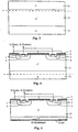
- Fig. 3 outlines a section of a wafer cross-section after the preliminary technological process of the starting material based on the inventive solution.
- a bilateral deep n-type diffusion 14, 15 is introduced into the homogeneously n - -doped Si wafer (13).
- the penetration depth of this n-doping is higher than would be necessary for the electrical operation of the stop layer.
- Practically well to be realized penetration depths are z. B. at about 150 microns. In principle, a one-sided diffusion would be sufficient, but it fails practically at the masking of the non-doping side.
- the n-doping (14) on the wafer top side is completely removed by abrading and the wafer subsequently polished, indicated by the dashed line in the n - - layer (13). Furthermore, the wafer backside is sealed to prevent auto-doping.
- the wafer thickness is now in a manageable for the production area, for example, for blocking voltages of 3500 volts at about 430 microns and for blocking voltages of 2500 volts at about 350 microns.
- the p-region (4) forms the DMOS channel of the IGBT or the base of an npn transistor, the n + - region (5) forms the emitter, the oxide layer (6) and the polysilicon layer (7) Gate of the entire component in IGBT structures.
- the wafer is abraded from the back, marked by the dashed line in the n-type doping layer (15).
- At least one of the introduced n-doping (15) remains such vertical expansion as a reserve, which prevents a punch-through breakthrough.
- a diffusion depth of the stop layer for example of 150 ⁇ m, can be reduced to approx. 25 ⁇ m (punch through reserve).
- Fig. 5 illustrates a section of the wafer finished on the back. Following the grinding of the back side of the wafer, the p-back emitter (12) is implanted from the back and activated. The remaining sketched configuration is described in FIG. 4.
- the method of forming the collector corresponds to the prior art that has hitherto been mainly applied to NPT IGBTs for producing the backside emitter.
- the collector (10) is located on the back of the wafer.
- the doping of the stop layer is relatively low (extensions of the diffusion region), so that the emitter efficiency and the charge carrier distribution in the n - - base region can be adjusted within wide ranges via the doping of the backside emitter.
- a low doping gradient between the stop layer and the backside emitter causes the flux voltage to increase as the switching losses and saturation currents decrease, and at a higher gradient the flux voltage decreases as the switching losses and saturation currents increase.
- RTP / RTA Rapid Thermal Processing / Rapid Thermal Annealing: processes for extremely short-term local Heating (possibly until melting) of the semiconductor material, with hardly any diffusion and a high activation of the dopants takes place), whereby an increased activation of the Dotand and thus a lower flux voltage is achieved.
- a significantly higher activation temperature can be selected here as 450 ° C, since no metallization layers can be thermally damaged.
- a retooling for thin Wafer is only necessary for those facilities that are responsible for the production and structuring of Al metallization and for the subsequent passivation layers are required.
Landscapes
- Electrodes Of Semiconductors (AREA)
- Crystals, And After-Treatments Of Crystals (AREA)
Description
Claims (7)
- Verfahren zur Herstellung eines Punch- Through- Leistungshalbleiterbauelements mit mindestens einem eine hohe Spannung sperrenden pn- Übergang ausgehend von einem monokristallinen Halbleiter-Wafer mit einer ersten Leitfähigkeit in niedriger Dotierung, wobei dieses Leistungshalbleiterbauelement eine Basiszone (13) dieser ersten Leitfähigkeit und niedriger Dotierung, eine Stoppschicht (15) der ersten Leitfähigkeit mit höherer Dotiertung, einen Emitter einer zweiten Leitfähigkeit auf der unterseite des Leistungshalbleiter bauelements und weitere Diffusionsgebiete (4,5) verschiedener Leitfähigkeit auf der Oberseite des Leistungshalbleiterbauelements aufweist,
mit den folgenden aufeinander folgenden Verarbeitungsschritten:gleichzeitige Diffusion der Stoppschicht (15) auf der Waferunterseite und einer weiteren Schicht (14) der ersten Leitfähigkeit auf der Waferoberseite, in den monokristallinen Halbleiter-Wafer;vollständiges Entfernen der weiteren Schicht (14) von der Waferoberseite;Ausbildung aller der obergenannten weiteren Diffusionsgebiete (4,5) auf der Waferoberseite zur Ausbildung der Funktionalität des Leistungshalbleiterbauelements;Verringern der Schichtdicke der Stoppschicht (15) auf der Waferunterseite;Ausbildung des Emitters (12) auf der Waferunterseite. - Verfahren nach Anspruch 1, dadurch gekennzeichnet, dass die Stoppschicht (15) und die weiteren Schicht (14) gleichzeitig ca. 150µm tief diffundiert werden.
- Verfahren nach Anspruch 1, dadurch gekennzeichnet, dass die weitere Schicht (14) mittels Schleifen und / oder Polieren entfernt wird.
- Verfahren nach Anspruch 1, dadurch gekennzeichnet, dass nach dem Entfernen der weiteren Schicht und vor dem Verringern der Schichtdicke der Stoppschicht weitere Prozessschritte zur Ausbildung einer Oxidschicht (6) und einer Polysiliziumschicht (7) erfolgen.
- Verfahren nach Anspruch 2, dadurch gekennzeichnet, dass die Verringerung der Schichtdicke der Stoppschicht (15) auf ca. 25µm erfolgt.
- Verfahren nach Anspruch 1, dadurch gekennzeichnet, dass der Emitter (12) mittels Implantation und Niedertemperatur- Ausheilung oder Niedertemperatur- Epitaxie hergestellt wird.
- Verfahren nach Anspruch 1, dadurch gekennzeichnet, dass der Emitter (12) mittels Einbringen von Dotanden und Aktivierung dieser Dotanden durch RTP/RTA-Verfahren hergestellt wird.
Applications Claiming Priority (2)
| Application Number | Priority Date | Filing Date | Title |
|---|---|---|---|
| DE19829614A DE19829614B4 (de) | 1998-07-02 | 1998-07-02 | Verfahren zur Herstellung eines Leistungshalbleiterbauelementes |
| DE19829614 | 1998-07-02 |
Publications (2)
| Publication Number | Publication Date |
|---|---|
| EP0969501A1 EP0969501A1 (de) | 2000-01-05 |
| EP0969501B1 true EP0969501B1 (de) | 2005-10-19 |
Family
ID=7872782
Family Applications (1)
| Application Number | Title | Priority Date | Filing Date |
|---|---|---|---|
| EP99112146A Expired - Lifetime EP0969501B1 (de) | 1998-07-02 | 1999-06-24 | Verfahren zur Herstellung von Leistungshalbleiterbauelementen |
Country Status (4)
| Country | Link |
|---|---|
| EP (1) | EP0969501B1 (de) |
| AT (1) | ATE307390T1 (de) |
| DE (2) | DE19829614B4 (de) |
| ES (1) | ES2251136T3 (de) |
Families Citing this family (12)
| Publication number | Priority date | Publication date | Assignee | Title |
|---|---|---|---|---|
| DE10055446B4 (de) * | 1999-11-26 | 2012-08-23 | Fuji Electric Co., Ltd. | Halbleiterbauelement und Verfahren zu seiner Herstellung |
| DE10024859A1 (de) | 2000-05-19 | 2001-12-06 | Infineon Technologies Ag | Schaltungsanordnung zum entlasteten Schalten |
| DE10031781A1 (de) * | 2000-07-04 | 2002-01-17 | Abb Semiconductors Ag Baden | Halbleiterbauelement und Verfahren zu dessen Herstellung |
| JP3764343B2 (ja) * | 2001-02-28 | 2006-04-05 | 株式会社東芝 | 半導体装置の製造方法 |
| DE10117483A1 (de) * | 2001-04-07 | 2002-10-17 | Bosch Gmbh Robert | Halbleiterleistungsbauelement und entsprechendes Herstellungsverfahren |
| JP2005057235A (ja) * | 2003-07-24 | 2005-03-03 | Mitsubishi Electric Corp | 絶縁ゲート型バイポーラトランジスタ及びその製造方法、並びに、インバータ回路 |
| DE102004039208B4 (de) | 2004-08-12 | 2014-01-16 | Infineon Technologies Ag | Verfahren zur Herstellung eines Leistungsbauelements mit einer vergrabenen n-dotierten Halbleiterzone und Leistungsbauelement |
| DE102004039209B4 (de) | 2004-08-12 | 2009-04-23 | Infineon Technologies Austria Ag | Verfahren zur Herstellung einer n-dotierten Feldstoppzone in einem Halbleiterkörper und Halbleiterbauelement mit einer Feldstoppzone |
| EP2045844A1 (de) * | 2007-10-03 | 2009-04-08 | ABB Technology AG | Halbleitermodul |
| EP2695193B1 (de) | 2011-04-06 | 2016-12-21 | ABB Technology AG | Bipolares pt-halbleiterbauelement und verfahren zur herstellung eines solchen halbleiterbauelements |
| EP2637210A1 (de) | 2012-03-05 | 2013-09-11 | ABB Technology AG | Leistungshalbleiterbauelement und Verfahren zu seiner Herstellung |
| CN104332495B (zh) * | 2013-07-22 | 2017-12-15 | 无锡华润上华科技有限公司 | 一种绝缘栅双极晶体管及其制造方法 |
Citations (1)
| Publication number | Priority date | Publication date | Assignee | Title |
|---|---|---|---|---|
| JPS60145660A (ja) * | 1984-01-09 | 1985-08-01 | Mitsubishi Electric Corp | 半導体装置の製造方法 |
Family Cites Families (10)
| Publication number | Priority date | Publication date | Assignee | Title |
|---|---|---|---|---|
| DE3884652D1 (de) * | 1987-04-07 | 1993-11-11 | Bbc Brown Boveri & Cie | Gate-Ausschaltthyristor und Verfahren zu dessen Herstellung. |
| EP0313000B1 (de) * | 1987-10-21 | 1998-05-06 | Siemens Aktiengesellschaft | Verfahren zum Herstellen eines Bipolartransistors mit isolierter Gateelektrode |
| JPH0648729B2 (ja) * | 1988-02-24 | 1994-06-22 | シーメンス、アクチエンゲゼルシシヤフト | 電界効果制御可能のバイポーラ・トランジスタ |
| JPH0724312B2 (ja) * | 1988-06-10 | 1995-03-15 | 三菱電機株式会社 | 半導体装置の製造方法 |
| JPH02312280A (ja) * | 1989-05-26 | 1990-12-27 | Mitsubishi Electric Corp | 絶縁ゲート型バイポーラトランジスタ |
| JPH04286163A (ja) * | 1991-03-14 | 1992-10-12 | Shin Etsu Handotai Co Ltd | 半導体基板の製造方法 |
| JP2878488B2 (ja) * | 1991-07-10 | 1999-04-05 | 三菱電機株式会社 | 半導体基板の製造方法 |
| JPH05347413A (ja) * | 1992-06-12 | 1993-12-27 | Toshiba Corp | 半導体装置の製造方法 |
| JP2911694B2 (ja) * | 1992-10-29 | 1999-06-23 | 信越半導体株式会社 | 半導体基板及びその製造方法 |
| DE4313170A1 (de) * | 1993-04-22 | 1994-10-27 | Abb Management Ag | Leistungshalbleiterbauelement |
-
1998
- 1998-07-02 DE DE19829614A patent/DE19829614B4/de not_active Expired - Lifetime
-
1999
- 1999-06-24 AT AT99112146T patent/ATE307390T1/de active
- 1999-06-24 DE DE59912665T patent/DE59912665D1/de not_active Expired - Lifetime
- 1999-06-24 ES ES99112146T patent/ES2251136T3/es not_active Expired - Lifetime
- 1999-06-24 EP EP99112146A patent/EP0969501B1/de not_active Expired - Lifetime
Patent Citations (1)
| Publication number | Priority date | Publication date | Assignee | Title |
|---|---|---|---|---|
| JPS60145660A (ja) * | 1984-01-09 | 1985-08-01 | Mitsubishi Electric Corp | 半導体装置の製造方法 |
Non-Patent Citations (1)
| Title |
|---|
| PATENT ABSTRACTS OF JAPAN vol. 009, no. 310 (E - 364) 6 December 1985 (1985-12-06) * |
Also Published As
| Publication number | Publication date |
|---|---|
| DE59912665D1 (de) | 2006-03-02 |
| ATE307390T1 (de) | 2005-11-15 |
| EP0969501A1 (de) | 2000-01-05 |
| ES2251136T3 (es) | 2006-04-16 |
| DE19829614A1 (de) | 2000-01-13 |
| DE19829614B4 (de) | 2004-09-23 |
Similar Documents
| Publication | Publication Date | Title |
|---|---|---|
| DE102015208097B4 (de) | Herstellen einer Halbleitervorrichtung durch Epitaxie | |
| DE69120995T2 (de) | Hochgeschwindigkeitsdiode und Verfahren zur Herstellung | |
| DE10207522B4 (de) | Halbleiterbauelement und Verfahren zu dessen Herstellung | |
| DE102008048832B4 (de) | Halbleitervorrichtung | |
| DE102007030805B4 (de) | Halbleitervorrichtung und Herstellungsverfahren derselben | |
| DE102018132236B4 (de) | Leistungshalbleiterbauelement und Verfahren zu dessen Herstellung | |
| DE112010004241T5 (de) | Halbleiterbauelement und Verfahren zur Herstellung des Halbleiterbauelements | |
| DE102022102521B4 (de) | Halbleitervorrichtung und Verfahren zum Herstellen derselben | |
| DE112013001297B4 (de) | Verfahren zur Herzustellung einer Leistungshalbleitervorrichtung | |
| DE102014108279A1 (de) | Halbleitervorrichtung mit rekombinationszentren und herstellungsverfahren | |
| DE102015100340A1 (de) | Bipolare halbleitervorrichtung und herstellungsverfahren dafür | |
| CN101884106A (zh) | 半导体模块 | |
| EP1307923B1 (de) | Hochvolt-diode und verfahren zu deren herstellung | |
| DE112013002031T5 (de) | Halbleitervorrichtung und Halbleitervorrichtungsherstellungsverfahren | |
| DE3037316A1 (de) | Verfahren zur herstellung von leistungs-schaltvorrichtungen | |
| DE102005043913B4 (de) | Verfahren zur Herstellung einer dotierten Zone in einem Halbleiterkörper | |
| DE102014103325A1 (de) | Leistungsschaltmodul mit verringerter Oszillation und Verfahren zur Herstellung einer Leistungsschaltmodulschaltung | |
| DE112013002751T5 (de) | Leistungshalbleitervorrichtung vom Typ mit hochspannungsisoliertem Gate und Verfahren zum Herstellen derselben | |
| DE102006047244B4 (de) | Halbleiterbauelement mit einem monokristallinen Halbleiterkörper und Verfahren zur Herstellung desselben | |
| DE19829614B4 (de) | Verfahren zur Herstellung eines Leistungshalbleiterbauelementes | |
| DE112020002222T5 (de) | Siliziumkarbid-halbleitervorrichtung und verfahren zum herstellen einer siliziumkarbid-halbleitervorrichtung | |
| DE102009044670B4 (de) | Bipolares Halbleiterbauelement und Herstellungsverfahren | |
| DE112012001986B4 (de) | Bipolares Punch-Through-Halbleiterbauelement und Verfahren zur Herstellung eines derartigen Halbleiterbauelements | |
| DE112006001791B4 (de) | Non-Punch-Through Hochspannungs-IGBT für Schaltnetzteile und Verfahren zur Herstellung derselben | |
| DE102005039564B4 (de) | Verfahren zum Herstellen eines Halbleiterbauteils |
Legal Events
| Date | Code | Title | Description |
|---|---|---|---|
| PUAI | Public reference made under article 153(3) epc to a published international application that has entered the european phase |
Free format text: ORIGINAL CODE: 0009012 |
|
| AK | Designated contracting states |
Kind code of ref document: A1 Designated state(s): AT CH DE ES FR GB IT LI SE |
|
| AX | Request for extension of the european patent |
Free format text: AL;LT;LV;MK;RO;SI |
|
| 17P | Request for examination filed |
Effective date: 19991217 |
|
| AKX | Designation fees paid |
Free format text: AT CH DE ES FR GB IT LI SE |
|
| 17Q | First examination report despatched |
Effective date: 20020117 |
|
| GRAP | Despatch of communication of intention to grant a patent |
Free format text: ORIGINAL CODE: EPIDOSNIGR1 |
|
| GRAS | Grant fee paid |
Free format text: ORIGINAL CODE: EPIDOSNIGR3 |
|
| RAP1 | Party data changed (applicant data changed or rights of an application transferred) |
Owner name: SEMIKRON ELEKTRONIK GMBH & CO. KG |
|
| GRAA | (expected) grant |
Free format text: ORIGINAL CODE: 0009210 |
|
| AK | Designated contracting states |
Kind code of ref document: B1 Designated state(s): AT CH DE ES FR GB IT LI SE |
|
| REG | Reference to a national code |
Ref country code: GB Ref legal event code: FG4D Free format text: NOT ENGLISH |
|
| REG | Reference to a national code |
Ref country code: CH Ref legal event code: EP |
|
| REG | Reference to a national code |
Ref country code: CH Ref legal event code: NV Representative=s name: BRAUNPAT BRAUN EDER AG |
|
| REG | Reference to a national code |
Ref country code: SE Ref legal event code: TRGR |
|
| GBT | Gb: translation of ep patent filed (gb section 77(6)(a)/1977) |
Effective date: 20060104 |
|
| REF | Corresponds to: |
Ref document number: 59912665 Country of ref document: DE Date of ref document: 20060302 Kind code of ref document: P |
|
| REG | Reference to a national code |
Ref country code: ES Ref legal event code: FG2A Ref document number: 2251136 Country of ref document: ES Kind code of ref document: T3 |
|
| ET | Fr: translation filed | ||
| PLBE | No opposition filed within time limit |
Free format text: ORIGINAL CODE: 0009261 |
|
| STAA | Information on the status of an ep patent application or granted ep patent |
Free format text: STATUS: NO OPPOSITION FILED WITHIN TIME LIMIT |
|
| 26N | No opposition filed |
Effective date: 20060720 |
|
| REG | Reference to a national code |
Ref country code: FR Ref legal event code: PLFP Year of fee payment: 18 |
|
| REG | Reference to a national code |
Ref country code: FR Ref legal event code: PLFP Year of fee payment: 19 |
|
| REG | Reference to a national code |
Ref country code: CH Ref legal event code: PCAR Free format text: NEW ADDRESS: HOLEESTRASSE 87, 4054 BASEL (CH) |
|
| REG | Reference to a national code |
Ref country code: FR Ref legal event code: PLFP Year of fee payment: 20 |
|
| PGFP | Annual fee paid to national office [announced via postgrant information from national office to epo] |
Ref country code: DE Payment date: 20180630 Year of fee payment: 20 Ref country code: CH Payment date: 20180626 Year of fee payment: 20 |
|
| PGFP | Annual fee paid to national office [announced via postgrant information from national office to epo] |
Ref country code: FR Payment date: 20180625 Year of fee payment: 20 Ref country code: AT Payment date: 20180620 Year of fee payment: 20 |
|
| PGFP | Annual fee paid to national office [announced via postgrant information from national office to epo] |
Ref country code: SE Payment date: 20180626 Year of fee payment: 20 |
|
| PGFP | Annual fee paid to national office [announced via postgrant information from national office to epo] |
Ref country code: ES Payment date: 20180723 Year of fee payment: 20 Ref country code: IT Payment date: 20180622 Year of fee payment: 20 Ref country code: GB Payment date: 20180626 Year of fee payment: 20 |
|
| REG | Reference to a national code |
Ref country code: DE Ref legal event code: R071 Ref document number: 59912665 Country of ref document: DE |
|
| REG | Reference to a national code |
Ref country code: CH Ref legal event code: PL |
|
| REG | Reference to a national code |
Ref country code: GB Ref legal event code: PE20 Expiry date: 20190623 |
|
| REG | Reference to a national code |
Ref country code: SE Ref legal event code: EUG |
|
| REG | Reference to a national code |
Ref country code: AT Ref legal event code: MK07 Ref document number: 307390 Country of ref document: AT Kind code of ref document: T Effective date: 20190624 |
|
| PG25 | Lapsed in a contracting state [announced via postgrant information from national office to epo] |
Ref country code: GB Free format text: LAPSE BECAUSE OF EXPIRATION OF PROTECTION Effective date: 20190623 |
|
| REG | Reference to a national code |
Ref country code: ES Ref legal event code: FD2A Effective date: 20200904 |
|
| PG25 | Lapsed in a contracting state [announced via postgrant information from national office to epo] |
Ref country code: ES Free format text: LAPSE BECAUSE OF EXPIRATION OF PROTECTION Effective date: 20190625 |