EP0966017B1 - Gasentladungs-Anzeigevorrichtung - Google Patents
Gasentladungs-Anzeigevorrichtung Download PDFInfo
- Publication number
- EP0966017B1 EP0966017B1 EP99301043A EP99301043A EP0966017B1 EP 0966017 B1 EP0966017 B1 EP 0966017B1 EP 99301043 A EP99301043 A EP 99301043A EP 99301043 A EP99301043 A EP 99301043A EP 0966017 B1 EP0966017 B1 EP 0966017B1
- Authority
- EP
- European Patent Office
- Prior art keywords
- filter
- display device
- light
- gas discharge
- discharge
- Prior art date
- Legal status (The legal status is an assumption and is not a legal conclusion. Google has not performed a legal analysis and makes no representation as to the accuracy of the status listed.)
- Expired - Lifetime
Links
Images




Classifications
-
- H—ELECTRICITY
- H01—ELECTRIC ELEMENTS
- H01J—ELECTRIC DISCHARGE TUBES OR DISCHARGE LAMPS
- H01J11/00—Gas-filled discharge tubes with alternating current induction of the discharge, e.g. alternating current plasma display panels [AC-PDP]; Gas-filled discharge tubes without any main electrode inside the vessel; Gas-filled discharge tubes with at least one main electrode outside the vessel
- H01J11/10—AC-PDPs with at least one main electrode being out of contact with the plasma
- H01J11/12—AC-PDPs with at least one main electrode being out of contact with the plasma with main electrodes provided on both sides of the discharge space
-
- C—CHEMISTRY; METALLURGY
- C09—DYES; PAINTS; POLISHES; NATURAL RESINS; ADHESIVES; COMPOSITIONS NOT OTHERWISE PROVIDED FOR; APPLICATIONS OF MATERIALS NOT OTHERWISE PROVIDED FOR
- C09K—MATERIALS FOR MISCELLANEOUS APPLICATIONS, NOT PROVIDED FOR ELSEWHERE
- C09K11/00—Luminescent materials, e.g. electroluminescent or chemiluminescent
- C09K11/08—Luminescent materials, e.g. electroluminescent or chemiluminescent containing inorganic luminescent materials
-
- H—ELECTRICITY
- H01—ELECTRIC ELEMENTS
- H01J—ELECTRIC DISCHARGE TUBES OR DISCHARGE LAMPS
- H01J11/00—Gas-filled discharge tubes with alternating current induction of the discharge, e.g. alternating current plasma display panels [AC-PDP]; Gas-filled discharge tubes without any main electrode inside the vessel; Gas-filled discharge tubes with at least one main electrode outside the vessel
- H01J11/20—Constructional details
- H01J11/34—Vessels, containers or parts thereof, e.g. substrates
- H01J11/36—Spacers, barriers, ribs, partitions or the like
-
- H—ELECTRICITY
- H01—ELECTRIC ELEMENTS
- H01J—ELECTRIC DISCHARGE TUBES OR DISCHARGE LAMPS
- H01J11/00—Gas-filled discharge tubes with alternating current induction of the discharge, e.g. alternating current plasma display panels [AC-PDP]; Gas-filled discharge tubes without any main electrode inside the vessel; Gas-filled discharge tubes with at least one main electrode outside the vessel
- H01J11/20—Constructional details
- H01J11/34—Vessels, containers or parts thereof, e.g. substrates
- H01J11/38—Dielectric or insulating layers
-
- H—ELECTRICITY
- H01—ELECTRIC ELEMENTS
- H01J—ELECTRIC DISCHARGE TUBES OR DISCHARGE LAMPS
- H01J11/00—Gas-filled discharge tubes with alternating current induction of the discharge, e.g. alternating current plasma display panels [AC-PDP]; Gas-filled discharge tubes without any main electrode inside the vessel; Gas-filled discharge tubes with at least one main electrode outside the vessel
- H01J11/20—Constructional details
- H01J11/34—Vessels, containers or parts thereof, e.g. substrates
- H01J11/44—Optical arrangements or shielding arrangements, e.g. filters, black matrices, light reflecting means or electromagnetic shielding means
-
- H—ELECTRICITY
- H01—ELECTRIC ELEMENTS
- H01J—ELECTRIC DISCHARGE TUBES OR DISCHARGE LAMPS
- H01J5/00—Details relating to vessels or to leading-in conductors common to two or more basic types of discharge tubes or lamps
- H01J5/02—Vessels; Containers; Shields associated therewith; Vacuum locks
- H01J5/16—Optical or photographic arrangements structurally combined with the vessel
-
- H—ELECTRICITY
- H01—ELECTRIC ELEMENTS
- H01J—ELECTRIC DISCHARGE TUBES OR DISCHARGE LAMPS
- H01J2211/00—Plasma display panels with alternate current induction of the discharge, e.g. AC-PDPs
- H01J2211/20—Constructional details
- H01J2211/22—Electrodes
- H01J2211/24—Sustain electrodes or scan electrodes
- H01J2211/245—Shape, e.g. cross section or pattern
Definitions
- the present invention relates to a gas discharge display device, and more particularly to a plasma display device incorporating a PDP (Plasma Display Panel).
- PDP Plasma Display Panel
- PDPs are becoming more and more popular as a means for television display on a large screen since their practical application to color display started.
- One of the problems related to image quality of PDPs is an enlargement of a reproducible color range.
- AC-type PDPs with a three-electrode surface-discharge structure have become commercialized as color display devices.
- the three-electrode AC surface-discharge PDPs have pairs of main electrodes arranged parallel to each other on individual lines (rows) of matrix display for sustaining light-emission, and address electrodes arranged one by one on individual columns. Ribs for preventing discharge interference among discharge cells are provided in a stripe pattern.
- fluorescent layers for color display can be provided on a substrate opposed to the substrate on which the main electrode pairs are placed, and thereby it is possible to prevent the fluorescent layers from being deteriorated by ion impact at electric discharges and to increase the life of the devices.
- a PDP having the fluorescent layers on a rear substrate is called a "reflection type”
- the one having the fluorescent layers on a front substrate is called a "projection type”.
- the reflection-type PDP is superior to the projection-type PDP in light-emission efficiency.
- a Penning gas containing neon (Ne) mixed with a little amount (4 to 5%) of xenon (Xe) has previously been considered for use as a discharge gas.
- the discharge gas When electric discharge occurs among the main electrodes, the discharge gas emits an ultraviolet light, which in turn excites a fluorescent substance to emit light.
- Each pixel corresponds to three cells, and a display color is determined and set by controlling the amounts of light-emission of the fluorescent substances of three colors of R (red), G (green), and B (blue).
- compositions of the fluorescent substances and a ratio of light-emission intensities of the three colors have been selected so that a white display color may be obtained when the amount of light-emission of each of R, G, and B is given the same signal strength.
- discharge gases include a three-component gas containing the above-mentioned Penning gas mixed with helium (He) or argon (Ar) (Ne + Xe + He, Ne + Xe + Ar), a two-component gas containing helium and xenon (He + Xe), and a three-component gas containing helium, argon, and xenon (He + Ar + Xe).
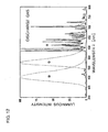
- Fig. 12 is a view showing an emission spectrum of a two-component gas containing neon and xenon.
- examples of emission peaks of R, G, and B fluorescent substances are shown by broken lines.
- the emission peak of the discharge gas is located near the maximum emission peak (590 nm) of the R fluorescent substance. Therefore, the red color generated by light-emission of the discharge gas is added irrespective of the color reproduced by the fluorescent substances, whereby a reddish display will appear on the entire screen. In other words, the capability of displaying the blue and green colors will decrease.
- the display color of a white pixel will be a color having a lower color temperature than the color reproduced by the fluorescent substances of the three colors.
- EP-A-0814492 discloses a plasma display panel in which a separate color filter is formed in front of each fluorescent substance.
- a gas discharge display device comprising: a plasma display panel having a plurality of discharge cells formed within a discharge space between a front substrate and a rear substrate, each of the discharge cells including a discharge gas therein and being provided with one of fluorescent substances of red, green and blue selected to emit light for performing color display; and a filter disposed on a front side of the front substrate, characterised in that the filter has a characteristic of absorbing light within a wavelength range of visible light emitted by the discharge gas, and a light-emission intensity of at least one of the fluorescent substances of red, green and blue is set to be larger than would be necessary to display an intended white color by simultaneous unfiltered light emission of the fluorescent substances of red, green and blue, so that light within said wavelength range is emitted with an intensity which compensates for the attenuation of light within the wavelength range absorbed by the filter.
- a filter is disposed for attenuating a light emitted by a discharge gas.
- the white color balance of the color reproduction by the fluorescent substances is intentionally shifted from the optimal value beforehand. For example, if a discharge gas emitting a light having a spectrum shown in Fig. 12 is to be used, the influence of light-emission of the discharge gas can be reduced by employing a red-cutting filter. This is disclosed as a side effect accompanying a shield of near infrared light in Japanese Unexamined Patent Publication No. HEI 09(1997)-145918.
- the capability of displaying a red color will decrease because the light of a red region emitted by the fluorescent substance will also be attenuated, even though the display color of the white pixel can be shifted to a blue side on a chromaticity diagram. It is extremely difficult to selectively exclude only the color emitted by the discharge gas.
- the emission of light from the fluorescent substances is controlled so that the light within a wavelength region attenuated by the filter will be emitted at an intensity which is stronger by an amount attenuated by the filter.
- the amount of red light may be set to be a little larger among the fluorescent substances of R, G and B.
- Examples of the ways for allowing the amount of light emitted by a fluorescent substance of one color to be larger than those by the fluorescent substances of the other two colors include adoption of a material having a high luminance and increase of discharge intensity or light-emission area by changing an element structure. Element structures corresponding to the fluorescent substances of the three colors may be made different from each other to provide difference in the amount of light emission.
- An embodiment of the present invention can provide a gas discharge display device for displaying a color image by means of first, second and third fluorescent substances having different emission colors, wherein a color to be reproduced by light-emission of the first to third fluorescent substances for displaying a white pixel is set to be different from a white color intended for display, and a filter is disposed on a front side of the first to third fluorescent substances for approximating a display color of the white pixel to the white color intended for display.
- a structural condition of a display element corresponding to the first fluorescent substance may be different from structural conditions of other display elements, and a light-emission intensity of the display element corresponding to the first fluorescent substance may be higher than a light-emission intensity of the display element corresponding to the first fluorescent substance which intensity is required in reproducing a white color intended for display by means of light emission of the display elements corresponding to the first to third fluorescent substances.
- each of the display elements may comprise a pair of electrodes for display discharge, a fluorescent substance layer that emits light by means of electric discharge between the electrodes, and dielectric substance layers that cover the respective electrodes, and the structural condition may be an area of the electrodes.
- the structural condition may be an area of a light-emission region of the fluorescent substance layer.
- the structural condition may be a thickness of the dielectric layers.
- a light-emission intensity of a display element corresponding to the first fluorescent substance may be higher than a light-emission intensity of the display element corresponding to the first fluorescent substance which intensity is required in reproducing a white color intended for display by means of light-emission of the display elements corresponding to the first to third fluorescent substances.
- the filter may have a color correction function for increasing a color temperature value.
- the filter may have a characteristic of attenuating an intensity of light in a red wavelength region.
- the filter may have a characteristic such that an average transmissivity of light in a green wavelength region is lower than an average transmissivity of light in a blue wavelength region and higher than an average transmissivity of light in a red wavelength region.
- the filter may have a characteristic such that a transmissivity of a shorter wavelength side of a red wavelength region is higher than a transmissivity of a longer wavelength side of the red wavelength region.
- the filter may have a characteristic such that a wavelength providing the lowest transmissivity has a value within a range of 560 to 610 nanometers.
- the filter may have a characteristic such that absorption peaks appear at least in a wavelength region of 470 to 520 nanometers and in a wavelength region of 560 to 610 nanometers.
- a gas discharge display device embodying the present invention may comprise a substrate that constitutes a display surface with display elements, and the filter may be formed directly on the substrate.
- a gas discharge display device embodying the present invention may comprise a display panel incorporating a discharge space therein with arranged display elements, and the filter may be fabricated separately from the display panel and disposed on a front side of the display panel.
- the filter may be a pigment filter.
- the filter may be a multi-layer film filter.
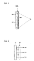
- Fig. 1 is a view illustrating a construction of a plasma display device 100 embodying the present invention.
- Fig. 2 is a model view illustrating a filter function.
- Fig. 3 is a view illustrating a construction of another plasma display device 200 embodying the present invention.
- the plasma display device 100 includes a PDP 1 as a color display panel, a filter 51 formed in close contact with a front surface of the PDP 1, a driving unit 80 for activating (i.e. lighting) each cell in the PDP 1 in accordance with display contents, and an external cover 90.
- the PDP 1 emits lights L R , L G , L B of three colors of R, G, B by light-emission of fluorescent substances, and a light L g by light-emission of a discharge gas.
- the filter 51 is designed to have a dimension extending over an entire display surface and an optical characteristic such that the filter 51 selectively attenuates the light L g . Referring to Fig.
- the plasma display device 200 includes a PDP 1b having the same structure as the PDP 1 and a filter 52 disposed on a front side of the PDP 1b.
- the filter 52 is fabricated separately from the PDP 1b and fixed to the PDP 1b or a frame of a device housing by means of a support (not shown).
- the filter 52 also has a characteristic to attenuate the light emitted by the discharge gas.
- a pigment filter utilizing a light absorption by a pigment, a multi-layer film filter utilizing an interference of a multi-layer film, or a different kind of filter may be used as the filter 51 and the filter 52.
- Fig. 4 is an exploded perspective view illustrating a fundamental structure inside the PDP 1.
- the PDP 1 is a three-electrode surface discharge PDP in which pairs of first and second main electrodes X and Y are disposed in parallel for generating an electric discharge for sustaining light-emission, and define cells (display elements) at intersections of the main electrodes X, Y with address electrodes A as third electrodes.
- the main electrodes X and Y extend in the direction of lines, i.e. in the horizontal direction, on the screen.
- the second main electrodes Y are used as scanning electrodes to select cells line by line in addressing.
- the address electrodes A extend in the direction of columns, i.e. in the vertical direction, and are used as data electrodes to select cells column by column in the addressing.
- a region on a substrate surface where the main electrodes intersect with the address electrodes is a display surface.
- a pair of main electrodes X and Y is disposed on each line on an inside surface of a glass substrate 11 which is a base member for a front-side substrate assembly.
- the line is a row of cells in the horizontal direction on the screen.
- the main electrodes X and Y each include an electrically conductive transparent film 41 and a metal film (bus conductor) 42 and is covered with a dielectric layer 17 of a low melting point glass of about 30 ⁇ m thickness.
- a protection film 18 of magnesia (MgO) of several thousand ⁇ thickness is disposed on a surface of the dielectric layer 17.
- the address electrodes A are arranged on an inside surface of a glass substrate 21 which is a base member for a rear-side substrate assembly.
- the address electrodes A are covered with a dielectric layer 24 of about 10 ⁇ m thickness.
- ribs 29 of about 150 ⁇ m height are each disposed between the address electrodes A.
- the ribs 29 are in the form of a linear band in a plan view. These ribs 29 partition a discharge space 30 for each sub-pixel (a unit light-emission area) in the row direction and also define a gap dimension for the discharge space 30.
- Fluorescent layers 28R, 28G, and 28B of three colors R, G, and B for color display are formed to cover a rear-side inner surface including a portion above the address electrodes A and side walls of the ribs 29.
- Preferable examples of the fluorescent substances are shown in Table 1. Emission color Fluorescent substance R (Y, Gd) BO 3 : Eu G Zn 2 SiO 4 : Mn B BaMgAl 10 O 17 : Eu
- the discharge space 30 is filled with a discharge gas containing neon as a main component with which xenon (4 to 5%) is mixed.
- the fluorescent layers 28R, 28G, and 28B are locally excited to emit light by ultraviolet rays radiated by xenon when an electric discharge takes place.
- the relative ratio of the maximum luminous intensities of R, G, and B in an embodiment of the present invention is set in such a manner that the luminous intensity within the attenuated wavelength region is a little stronger in order to compensate for the attenuation caused by the filter 51 or filter 52 so as to attain the best reproducibility of white color. In other words, if the filter 51 or 52 were not provided, a color different from that of the original image would be reproduced.
- the relative ratio of the luminous intensities is set by selecting the materials to be used for the fluorescent layers 28R, 28G, and 28B.
- One pixel for display is composed of three sub-pixels adjacently placed in the row direction and having different emission colors.
- a structural unit of each sub-pixel is a cell (a display element). Since the ribs 29 are arranged in a stripe pattern, portions of the discharge space 30 which correspond to the individual columns are continuous in the column direction, bridging all the lines.
- the gap of the electrodes between adjacent lines is set at a value which is sufficiently larger than the surface discharge gap (for example, a value within the range of 80 to 140 ⁇ m) and which can prevent charge coupling in the column direction (for example, a value within the range of 400 to 500 ⁇ m).
- An addressing discharge is generated between the main electrode Y and the address electrode A in a cell to be activated (in the case of a writing address form) or in a cell to be inactivated (in the case of an erasing address form) to form a charged state in which a suitable amount of wall charge is present only on cells to be activated for each line.
- an activation-sustaining voltage Vs is applied between the main electrodes X, Y to generate a surface discharge along the substrate surface in the cells to be activated.
- the filters 51, 52 have a characteristic of attenuating an intensity of light in a red wavelength region.
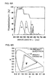
- Figs. 5A and 5B are views showing a first example of a filter characteristic and a range of color reproduction.
- the transmissivity characteristic of the filter 51 or the filter 52 is shown by a thick solid line and a light emission spectrum distributions of the fluorescent layers are shown by thin solid lines as a reference.
- Fig. 5B is a view showing a chromaticity diagram, wherein the black solid circle represents the white color displayed by application of an embodiment of the present invention.
- Fig. 5B the blank square represents a white color displayed using a previously-considered PDP and the broken line shows a range of color reproduction using a previously-considered PDP.
- the later-mentioned Figs. 6A and 6B to 8A and 8B are drawn in the same manner as in Figs. 5A and 5B.
- the filter characteristic shown in the example of Figs. 5A and 5B is such that the transmissivities of the visible light beams in the emission wavelength region of the R (red) fluorescent substance and in a region of emission wavelength longer than the above (i.e. the emission wavelength region of neon) are lower than the average transmissivity in the other visible light wavelength region.
- the filters 51, 52 have a characteristic such that an average transmissivity of light in a green wavelength region is lower than an average transmissivity of light in a blue wavelength region and higher than an average transmissivity of light in a red wavelength region.
- Figs. 6A and 6B are views showing a second example of a filter characteristic and a range of color reproduction.
- the filter characteristic shown in the example of Figs. 6A and 6B is such that the transmissivity of visible light beams in the red wavelength region is the same as that shown in Figs. 5A and 5B, and the average transmissivity of visible light beams in the wavelength region of the G fluorescent substance is lower than the average transmissivity of visible light beams in the wavelength region of the B fluorescent substance and is higher than the average transmissivity of visible light beams in the wavelength region of the R fluorescent substance.
- This may optimize the chromaticity of the white color display and the color temperature value to a greater degree than the example shown in Figs. 5A and 5B.
- the chromaticity of each color in Fig. 6B is shown in Table 3 together with that of the previously-considered PDP.
- White Red Green Blue x y x y x y x y y Present invention 0.31 0.31 0.62 0.35 0.24 0.65 0.17 0.08
- the filters 51, 52 have a characteristic such that a transmissivity of a longer wavelength side of a red wavelength region is higher than a transmissivity of a shorter wavelength side of the red wavelength region.
- a transmissivity of a longer wavelength side of a red wavelength region is higher than a transmissivity of a shorter wavelength side of the red wavelength region.
- the filters 51, 52 have a characteristic such that a wavelength providing the lowest transmissivity has a value within a range of 560 to 610 nanometers; and in Figs.
- the filters 51, 52 have a characteristic such that absorption peaks appear at least in a wavelength region of 470 to 520 nanometers and in a wavelength region of 560 to 610 nanometers.
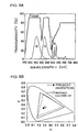
- Figs. 7A and 7B are views showing a third example of a filter characteristic and a range of color reproduction.
- the filter characteristic shown in the example of Figs. 7A and 7B is such that the filter shows an absorption peak within a region of 560 to 610 nm at which the emission peak of the discharge gas appears, thereby to efficiently remove the color emitted by the discharge gas.
- the filter has a characteristic such that the transmissivity of a longer wavelength side of the red wavelength region of the R fluorescent substance is higher than the transmissivity of a shorter wavelength side of the red wavelength region. This provides an effect that the light beams which are emitted by the R fluorescent substance and which does not overlap with the emission peak of the discharge gas can be effectively utilized for displaying, thereby improving the capability of expressing the red color.
- Figs. 8A and 8B are views showing a fourth example of a filter characteristic and a range of color reproduction.
- the filter characteristic shown in the example of Figs. 8A and 8B is such that the transmissivity of visible light beams in the red wavelength region is the same as that shown in Figs. 7A and 7B, and the filter shows an absorption peak in a wavelength region of 470 to 520 nanometers so as to clearly separate the emission of B color from the emission of G color. This may realize a display with excellent color purities of G and B in addition to an improvement in the reproducibility of white color.
- the chromaticity of each color in Fig. 8B is shown in Table 5 together with that of the previously-considered PDP.
- White Red Green Blue x y x y x y x y y Present invention 0.28 0.32 0.63 0.34 0.22 0.67 0.16 0.08
- the filter 51, 52 is disposed on the front side of the discharge space 30.
- the filter 51, 52 may be formed either directly on the outer surface of the glass substrate 11 or on a protection plate (reinforced glass or acrylic resin plate) disposed on the front side of the glass substrate 11 through the intermediary of an air layer (gap) having a thickness of about 1.5 to 6 mm for shutting off heat generated from the PDP.
- the base material may be a glass, an acrylic resin, a polycarbonate resin, a polymer film, or the like.
- the filter 51, 52 is preferably a film-like filter.
- a desired transmissivity characteristic may be made by dispersing a suitable pigment on a surface of a polymer film and pasting the obtained film-like filter on the glass substrate 11 or the protection film.
- the portion encircled by a chain line shows an example in which the film-like filter 53 is pasted on the inner surface of the protection plate 54 made of reinforced glass or acrylic resin plate.
- an electromagnetic shielding film 55 and a light-reflection preventive film 56 are further laminated in this order on the outer surface of the protection plate.
- the pigment that attenuates the light in the emission wavelength region of the discharge gas may be, for example, 1-ethyl-4-[(1-ethyl-4(1H)-quinolinylidene)methyl]quinolinium iodide having an absorption maximum at 590 nm (Product No. NK-6 manufactured by Nippon Kanko Shikiso Kenkyuosho Co., Ltd.
- the layers of the multi-layer film may be laminated by means of a thin film formation technique such as vapor deposition, sputtering, CVD, or the like.
- the emission of light in a wavelength region which is to be attenuated by the filter is increased (intensified) by selecting a material for the fluorescent substances while maintaining the cell structures for the R, G, and B colors to be the same.
- the ratio of the emission intensities of the R, G, and B colors is set by allowing the cells to have different cell structures.
- the area of the electrodes in the red display element is larger than an area of the electrodes in the red display element which area is required in reproducing the white color intended for display.
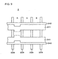
- Fig. 9 is a plan view illustrating an electrode structure of a PDP 2 according to a second embodiment of the present invention.
- the PDP 2 also has a three-electrode surface-discharge structure and its basic construction is the same as that of the PDP 1.
- a fluorescent layer (not shown) is disposed between adjacent ribs 229 arranged in a stripe-like pattern. Three consecutive cells arranged in parallel in the direction of arranging the ribs (i.e. in the row direction) constitute one pixel.
- the electrically-conductive transparent film 241 and the metal film 242, which constitute the main electrodes do not have uniform widths. Namely, the electrically conductive transparent film 241 above the R cells protrudes into the surface discharge gap and, in accordance therewith, the metal film 242 is formed to have a locally wider portion, as shown in Fig. 9.
- This structure allows the R cells to have a larger electrode area than the G cells or the B cells, whereby the discharge intensity of the R cells in this embodiment is increased as compared with the R cells of the previously-considered PDP in which the luminance ratio of R, G, and B is set to be a value (3 : 6 : 1) for reproducing the white color of intended display.
- the same effect may also be obtained by allowing only the electrically conductive transparent film 241 to have a locally wider portion.
- the area of the light-emission region of the fluorescent substance layer in the red display element is larger than an area of the light-emission region of the fluorescent substance layer in the red display element which area is required in reproducing the white color intended for display.
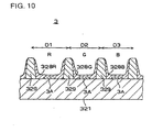
- Fig. 10 is a cross-sectional view illustrating part of a PDP 3 according to a third embodiment of the present invention.
- Address electrodes 3A and ribs 329 are arranged on a glass substrate 321 located on the rear side of the PDP 3, and fluorescent layers 328R, 328G, and 328B are formed between the ribs 329.
- the dimension D1 of the R cells in the line direction is longer than the each of the dimensions D2, D3 of the G cells and the B cells in the line direction.
- the emission area for the R color is larger than each of the emission areas for the G color and the B color to allow the R cells of this embodiment to generate a stronger discharge than the R cells of the previously-considered PDP.
- the thickness of the dielectric substance layers covering the electrodes in the red display element is smaller than a thickness of the dielectric substance layers covering the electrodes in the red display element which thickness is required in reproducing the white color intended for display.
- Fig. 11 is a cross-sectional view illustrating part of a PDP 4 according to a fourth embodiment of the present invention.
- Main electrodes 412 and a dielectric layer 417 are disposed on an inner surface of a glass substrate 411 located on the front side of the PDP 4.
- Address electrodes 4A and ribs 429 are arranged on a glass substrate 421 located on the rear side of the PDP 4, and fluorescent layers 428R, 428G, and 428B are formed between the ribs 429.
- the dielectric layer 417 above the R cells has a smaller thickness than the dielectric layer 417 above the G cells or the B cells, whereby the discharge intensity of the R cells in this embodiment is increased as compared with the R cells of the previously-considered PDP.
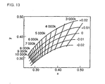
- Fig. 13 is cited from "Television Technology Handbook", Video Information Media Society ed., 1998, p. 20, and shows equi-color-temperature lines and equi-deviation lines on an x-y chromaticity diagram.
- a color temperature to be reproduced by light-emission of the first to third fluorescent substances for displaying white pixel is set to be about 1000K lower than the color temperature of white color intended for display to cut the color emitted from the discharge gas effectively.
- the preferable color temperature value varies in accordance with the system requirements or the region in which the device is used. For instance, in Japan, people prefer a color temperature value of about 9000K. However, the value of about 6000K is preferred in Europe and the United States of America.
- the filter characteristic may be set so that the color emitted by the discharge gas is removed and the emission intensity of the light in the wavelength region which is attenuated by the filter is increased.
- the filter for removing the color emitted by the discharge gas may be combined with individual built-in R, G, B filters that are disposed for improving the color purity in each of R, G, and B cells.
- the emission intensity of the R color may be increased by varying the voltages supplied to the electrodes instead of varying the cell structures as mentioned above.
- the present invention can also be applied in other embodiments to a display using a gas discharge device other than the PDP.
- a gas discharge display device embodying the present invention can reduce the influence of light-emission by discharge gas and increase the color reproducibility.
Landscapes
- Physics & Mathematics (AREA)
- Engineering & Computer Science (AREA)
- Plasma & Fusion (AREA)
- Electromagnetism (AREA)
- Chemical & Material Sciences (AREA)
- Inorganic Chemistry (AREA)
- Materials Engineering (AREA)
- Organic Chemistry (AREA)
- Gas-Filled Discharge Tubes (AREA)
Claims (19)
- Gasentladungs-Anzeigevorrichtung, umfassend:dadurch gekennzeichnet, dass der Filter eine Charakteristik aufweist, gemäß der Licht in einem Wellenlängenbereich des von dem Entladungsgas emittierten sichtbaren Lichts absorbiert wird, und dass eine Lichtemissions-Intensität von wenigstens einer der fluoreszierenden Substanzen von rot, grün und blau größer eingestellt ist, als es erforderlich wäre, um eine erwünschte weiße Farbe durch gleichzeitige ungefilterte Lichtemission der fluoreszierenden Substanzen von rot, grün und blau anzuzeigen, so dass das Licht in dem Wellenlängenbereich mit einer Intensität emittiert wird, welche die Dämpfung des Lichtes in dem durch den Filter absorbierten Wellenlängenbereich kompensiert.ein Plasma-Anzeigefeld (1) mit einer Vielzahl von Entladungszellen, welche in einem Entladungsraum (30) zwischen einem vorderen Substrat (11) und einem hinteren Substrat (21) ausgebildet sind, wobei jede der Entladungszellen ein Entladungsgas darin umfasst und versehen ist mit einer von fluoreszierenden Substanzen von rot, grün und blau, welche ausgewählt sind, um Licht zur Erzeugung einer Farbanzeige zu emittieren; undeinen Filter (31; 52), der auf einer Vorderseite des vorderen Substrats (11) angeordnet ist,
- Gasentladungs-Anzeigevorrichtung nach Anspruch 1, bei welcher die Lichtemissions-Intensität der roten fluoreszierenden Substanz größer eingestellt ist, als es erforderlich wäre, um eine erwünschte weiße Farbe durch gleichzeitige ungefilterte Lichtemission der fluoreszierenden Substanzen von rot, grün und blau anzuzeigen.
- Gasentladungs-Anzeigevorrichtung nach Anspruch 2, bei welcher jede der Entladungszellen ein Paar von Elektroden zur Erzeugung einer elektrischen Entladung zwischen den Elektroden aufweist, um zu ermöglichen, dass die fluoreszierenden Substanzen Licht emittieren, und jede der Entladungszellen mit der roten fluoreszierenden Substanz eine Fläche der Elektroden aufweist, die größer als diejenigen der Entladungszellen mit andersfarbigen fluoreszierenden Substanzen ist.
- Gasentladungs-Anzeigevorrichtung nach Anspruch 2, bei welcher jede der Entladungszellen mit roter fluoreszierender Substanz eine Fläche eines Lichtemissionsbereichs aufweist, die größer als diejenige der Entladungszellen mit andersfarbigen fluoreszierenden Substanzen ist.
- Gasentladungs-Anzeigevorrichtung nach Anspruch 2, bei welcher jede der Entladungszellen ein Paar von Elektroden zur Erzeugung einer elektrischen Entladung zwischen den Elektroden aufweist, um zu ermöglichen, dass die fluoreszierenden Substanzen Licht emittieren, sowie eine dielektrische Substanzschicht, welche die jeweiligen Elektroden bedeckt, wobei jede der Entladungszellen mit der roten fluoreszierenden Substanz eine Dicke der dielektrischen Substanzschicht aufweist, die kleiner als diejenige der Entladungszellen mit andersfarbigen fluoreszierenden Substanzen ist.
- Gasentladungs-Anzeigevorrichtung nach einem der Ansprüche 2 bis 5, bei welcher der Filter eine Farbkorrekturfunktion zur Erhöhung eines Farbtemperaturwerts aufweist.
- Gasentladungs-Anzeigevorrichtung nach einem der Ansprüche 2 bis 6, bei welcher der Filter eine Charakteristik zur Dämpfung einer Lichtintensität in einem roten Wellenlängenbereich aufweist.
- Gasentladungs-Anzeigevorrichtung nach einem der Ansprüche 2 bis 7, bei welcher der Filter eine Charakteristik derart aufweist, dass eine durchschnittliche Lichtdurchlässigkeit in einem grünen Wellenlängenbereich niedriger als eine durchschnittliche Lichtdurchlässigkeit in einem blauen Wellenlängenbereicht und höher als eine durchschnittliche Lichtdurchlässigkeit in einem roten Wellenlängenbereich ist.
- Gasentladungs-Anzeigevorrichtung nach einem der Ansprüche 2 bis 8, bei welcher der Filter eine Charakteristik derart aufweist, dass eine Durchlässigkeit auf der Seite mit längerer Wellenlänge eines roten wellenlängenbereichs größer ist als eine Durchlässigkeit auf einer Seite mit kürzerer Wellenlänge des roten Wellenlängenbereichs.
- Gasentladungs-Anzeigevorrichtung nach einem der Ansprüche 2 bis 9, bei welcher der Filter eine Charakteristik derart aufweist, dass eine Wellenlänge, welche die niedrigste Durchlässigkeit bereitstellt, einen Wert innerhalb eines Bereichs von 560 bis 610 Nanometer aufweist.
- Gasentladungs-Anzeigevorrichtung nach einem der Ansprüche 2 bis 10, bei welcher der Filter eine Charakteristik derart aufweist, dass die Absorptionsspitzen wenigstens in einem Wellenbereich von 470 bis 520 Nanometer und in einem Wellenbereich von 560 bis 610 Nanometer auftreten.
- Gasentladungs-Anzeigevorrichtung nach einem der vorhergehenden Ansprüche, bei welcher die Gasentladungs-Anzeigevorrichtung ein Paar von Substraten zum Ausbilden eines dazwischenliegenden Entladungsraums umfasst und der Filter direkt auf einer inneren und äußeren Fläche von einem der Substrate, welche eine Anzeigefläche bildet, ausgebildet ist.
- Gasentladungs-Anzeigevorrichtung nach einem der Ansprüche 1 bis 11, bei welcher die Gasentladungs-Anzeigevorrichtung ein Anzeigefeld umfasst, in dem ein Entladungsraum mit angeordneten Anzeigeelementen ausgebildet ist, und der Filter separat von dem Anzeigefeld hergestellt ist und auf einer Vorderseite des Anzeigefelds angeordnet ist.
- Gasentladungs-Anzeigevorrichtung nach einem der Ansprüche 1 bis 11, bei welcher die Gasentladungs-Anzeigevorrichtung umfasst ein Anzeigefeld, in dem ein Entladungsraum mit angeordneten Anzeigeelementen ausgebildet ist, und eine transparente Schutzplatte zum schutz einer Anzeigefläche des Anzeigefelds und bei welcher der Filter auf einer inneren und äußeren Fläche der Schutzplatte angeordnet ist.
- Gasentladungs-Anzeigevorrichtung nach einem der vorhergehenden Ansprüche, bei welcher der Filter ein Pigmentfilter ist.
- Gasentladungs-Anzeigevorrichtung nach einem der Ansprüche 1 bis 14, bei welcher der Filter ein Mehrschichtfilm-Filter ist.
- Gasentladungs-Anzeigevorrichtung nach einem der vorhergehenden Ansprüche, bei welcher die rote fluoreszierende Substanz eine fluoreszierende Substanz zusammengesetzt aus (Y, Gd) BO3 : Eu ist, die grüne fluoreszierende Substanz eine fluoreszierende Substanz zusammengesetzt aus Zn2SiO4 : Mn ist und die blaue fluoreszierende Substanz eine fluoreszierende Substanz zusammengesetzt aus BaMgAl10O17 : Eu ist.
- Gasentladungs-Anzeigevorrichtung nach einem der vorhergehenden Ansprüche, bei welcher das Entladungsgas ein Penning-Gas zusammengesetzt aus Neon und Xenon ist.
- Gasentladungs-Anzeigevorrichtung nach einem der vorhergehenden Ansprüche, bei welcher die Lichtemission von den fluoreszierenden Substanzen gesteuert wird, so dass Licht in einem Wellenlängenbereich, der durch den Filter absorbiert wird, mit einer Intensität emittiert wird, welche stärker als das Licht ist, welches in den anderen Wellenlängenbereichen emittiert wird.
Applications Claiming Priority (2)
| Application Number | Priority Date | Filing Date | Title |
|---|---|---|---|
| JP17117998A JP3410024B2 (ja) | 1998-06-18 | 1998-06-18 | ガス放電表示装置 |
| JP17117998 | 1998-06-18 |
Publications (3)
| Publication Number | Publication Date |
|---|---|
| EP0966017A2 EP0966017A2 (de) | 1999-12-22 |
| EP0966017A3 EP0966017A3 (de) | 2000-01-19 |
| EP0966017B1 true EP0966017B1 (de) | 2005-08-31 |
Family
ID=15918476
Family Applications (1)
| Application Number | Title | Priority Date | Filing Date |
|---|---|---|---|
| EP99301043A Expired - Lifetime EP0966017B1 (de) | 1998-06-18 | 1999-02-12 | Gasentladungs-Anzeigevorrichtung |
Country Status (5)
| Country | Link |
|---|---|
| US (3) | US6853125B1 (de) |
| EP (1) | EP0966017B1 (de) |
| JP (1) | JP3410024B2 (de) |
| KR (1) | KR100352864B1 (de) |
| DE (1) | DE69926956T2 (de) |
Families Citing this family (20)
| Publication number | Priority date | Publication date | Assignee | Title |
|---|---|---|---|---|
| JP4533538B2 (ja) * | 1998-10-20 | 2010-09-01 | 富士フイルム株式会社 | 光学フィルター |
| US20020005509A1 (en) * | 1999-01-21 | 2002-01-17 | Chia-Chi Teng | Dye combinations for image enhancement filters for color video displays |
| JP3864204B2 (ja) | 1999-02-19 | 2006-12-27 | 株式会社日立プラズマパテントライセンシング | プラズマディスプレイパネル |
| JP3589892B2 (ja) * | 1999-03-18 | 2004-11-17 | 富士通株式会社 | プラズマディスプレイパネル |
| JP3576032B2 (ja) * | 1999-03-31 | 2004-10-13 | 富士通株式会社 | ガス放電表示装置 |
| JP3625719B2 (ja) * | 1999-12-07 | 2005-03-02 | 富士通株式会社 | ガス放電表示装置 |
| JP2006058896A (ja) * | 2000-02-01 | 2006-03-02 | Mitsui Chemicals Inc | プラズマディスプレイ用フィルタ、表示装置およびその製造方法 |
| JP2001228323A (ja) * | 2000-02-14 | 2001-08-24 | Bridgestone Corp | 光学フィルタ及びプラズマディスプレイパネル |
| JP3576076B2 (ja) * | 2000-06-30 | 2004-10-13 | 松下電器産業株式会社 | 白色度評価方法及び照明用光源・照明装置 |
| JP4527862B2 (ja) * | 2000-09-04 | 2010-08-18 | 日立プラズマディスプレイ株式会社 | プラズマディスプレイパネル |
| JP2004101916A (ja) * | 2002-09-10 | 2004-04-02 | Fujitsu Hitachi Plasma Display Ltd | ガス放電表示装置 |
| KR20050106622A (ko) * | 2004-05-06 | 2005-11-11 | 엘지전자 주식회사 | 플라즈마 표시장치 및 그 제조방법 |
| JP2006059693A (ja) * | 2004-08-20 | 2006-03-02 | Fujitsu Ltd | 表示装置 |
| KR100667549B1 (ko) * | 2004-09-21 | 2007-01-12 | 엘지전자 주식회사 | 플라즈마 파이프를 포함하는 플라즈마 디스프레이 패널 |
| KR20060031560A (ko) * | 2004-10-08 | 2006-04-12 | 엘지전자 주식회사 | 스캔 전극과 서스테인 전극을 포함하는 플라즈마디스플레이 패널 |
| JP2008003508A (ja) * | 2006-06-26 | 2008-01-10 | Fujitsu Hitachi Plasma Display Ltd | ディスプレイ装置 |
| TWI312540B (en) * | 2006-10-11 | 2009-07-21 | Icf Technology Limite | Patterned thin-film layer and method for manufacturing same |
| US7839414B2 (en) * | 2007-07-30 | 2010-11-23 | Motorola Mobility, Inc. | Methods and devices for display color compensation |
| KR20090081596A (ko) * | 2008-01-24 | 2009-07-29 | 삼성에스디아이 주식회사 | 플라즈마 디스플레이 패널용 필터 및 이를 구비한 플라즈마디스플레이 장치 |
| CN111257268B (zh) * | 2020-03-23 | 2023-11-28 | 京东方科技集团股份有限公司 | 红外滤光装置及其制备方法、红外气体传感器 |
Family Cites Families (26)
| Publication number | Priority date | Publication date | Assignee | Title |
|---|---|---|---|---|
| JPS58153904A (ja) | 1982-03-08 | 1983-09-13 | Mitsubishi Rayon Co Ltd | プラスチツク系フイルタ− |
| JPS615202A (ja) * | 1984-06-20 | 1986-01-11 | Okuno Seiyaku Kogyo Kk | 赤色色光用無機素材光学フイルタ− |
| US4803402A (en) * | 1984-08-22 | 1989-02-07 | United Technologies Corporation | Reflection-enhanced flat panel display |
| US5024923A (en) * | 1987-09-09 | 1991-06-18 | Fuji Photo Film Co., Ltd. | Infrared absorbent compositions |
| US4990821A (en) * | 1988-06-27 | 1991-02-05 | Gte Products Corporation | Multicolor picture element with merged colors |
| US4989953A (en) * | 1989-01-24 | 1991-02-05 | Kirschner Kevin A | Video display terminal filter |
| EP0452922B1 (de) * | 1990-04-18 | 1997-01-29 | Matsushita Electric Industrial Co., Ltd. | Kompositschicht, Glaskompositmaterial und Verfahren zu seiner Herstellung |
| JPH0568257A (ja) | 1991-07-15 | 1993-03-19 | Canon Inc | カラー撮像装置 |
| JP3121090B2 (ja) | 1992-01-24 | 2000-12-25 | 富士通株式会社 | プラズマディスプレイパネル |
| JPH08123364A (ja) | 1994-10-20 | 1996-05-17 | Fujitsu General Ltd | 色補正装置 |
| JPH08190869A (ja) | 1994-11-08 | 1996-07-23 | Matsushita Electric Ind Co Ltd | プラズマディスプレイパネル |
| JP3719743B2 (ja) * | 1995-08-09 | 2005-11-24 | 株式会社日立製作所 | プラズマディスプレイパネル |
| JP3145279B2 (ja) * | 1995-08-28 | 2001-03-12 | 大日本印刷株式会社 | プラズマディスプレイパネル及びその製造方法 |
| JPH0992162A (ja) * | 1995-09-20 | 1997-04-04 | Hitachi Ltd | プラズマディスプレイパネル |
| JPH09145918A (ja) | 1995-11-22 | 1997-06-06 | Fujitsu General Ltd | フィルタ装置 |
| JP3145309B2 (ja) | 1996-06-12 | 2001-03-12 | 富士通株式会社 | 平面表示装置及びプラズマディスプレイパネルの近赤外線放出影響防止方法 |
| JP3116844B2 (ja) * | 1996-06-21 | 2000-12-11 | 日本電気株式会社 | カラープラズマディスプレイパネル、及びその製造方法 |
| US5834122A (en) | 1996-11-25 | 1998-11-10 | Hoechst Celanese Corp. | Spectrally tuned multiple bandpass filters for video displays |
| US6008582A (en) * | 1997-01-27 | 1999-12-28 | Dai Nippon Printing Co., Ltd. | Plasma display device with auxiliary partition walls, corrugated, tiered and pigmented walls |
| JP3039437B2 (ja) * | 1997-04-15 | 2000-05-08 | 日本電気株式会社 | カラープラズマディスプレイパネル |
| US5813753A (en) * | 1997-05-27 | 1998-09-29 | Philips Electronics North America Corporation | UV/blue led-phosphor device with efficient conversion of UV/blues light to visible light |
| US20020005509A1 (en) * | 1999-01-21 | 2002-01-17 | Chia-Chi Teng | Dye combinations for image enhancement filters for color video displays |
| JP2000323041A (ja) * | 1999-05-17 | 2000-11-24 | Hitachi Ltd | 表示用放電管 |
| JP2002056781A (ja) * | 2000-05-31 | 2002-02-22 | Mitsubishi Electric Corp | プラズマディスプレイパネル及びプラズマディスプレイ装置 |
| KR100391370B1 (ko) * | 2001-06-02 | 2003-07-16 | 주식회사옌트 | 교류형 플라즈마 디스플레이 패널의 색온도 향상을 위한제어 방법 및 장치 |
| EP2095421A2 (de) | 2006-07-27 | 2009-09-02 | Nanosolar Inc. | Individuell eingekapselte solarzellen und/oder solarzellenketten |
-
1998
- 1998-06-18 JP JP17117998A patent/JP3410024B2/ja not_active Expired - Fee Related
-
1999
- 1999-01-21 US US09/234,490 patent/US6853125B1/en not_active Expired - Fee Related
- 1999-01-28 KR KR1019990002650A patent/KR100352864B1/ko not_active Expired - Fee Related
- 1999-02-12 EP EP99301043A patent/EP0966017B1/de not_active Expired - Lifetime
- 1999-02-12 DE DE69926956T patent/DE69926956T2/de not_active Expired - Lifetime
-
2004
- 2004-09-14 US US10/939,420 patent/US7211952B2/en not_active Expired - Fee Related
-
2007
- 2007-03-12 US US11/716,596 patent/US20070152587A1/en not_active Abandoned
Also Published As
| Publication number | Publication date |
|---|---|
| KR100352864B1 (ko) | 2002-09-16 |
| JP2000011901A (ja) | 2000-01-14 |
| DE69926956D1 (de) | 2005-10-06 |
| US7211952B2 (en) | 2007-05-01 |
| KR20000005573A (ko) | 2000-01-25 |
| EP0966017A3 (de) | 2000-01-19 |
| JP3410024B2 (ja) | 2003-05-26 |
| US20050029943A1 (en) | 2005-02-10 |
| US6853125B1 (en) | 2005-02-08 |
| DE69926956T2 (de) | 2006-02-23 |
| EP0966017A2 (de) | 1999-12-22 |
| US20070152587A1 (en) | 2007-07-05 |
Similar Documents
| Publication | Publication Date | Title |
|---|---|---|
| US20070152587A1 (en) | Gas discharge display device with particular filter characteristics | |
| JP4838767B2 (ja) | プラズマディスプレイパネル | |
| JP2005063961A (ja) | プラズマディスプレイパネル | |
| EP1041598B1 (de) | Gasentladungs-Anzeigevorrichtung | |
| EP1107280B1 (de) | Gasentladungsanzeigevorrichtung | |
| KR20040087905A (ko) | 플라즈마 디스플레이 패널 | |
| JP3121090B2 (ja) | プラズマディスプレイパネル | |
| EP1067574B1 (de) | Plasma-Anzeigetafel | |
| US20060208636A1 (en) | Plasma display panel | |
| KR100551025B1 (ko) | 플라즈마 디스플레이 장치 | |
| JP2004527892A (ja) | カラーフィルタを有するプラズマカラーディスプレイスクリーン | |
| EP1398813A2 (de) | Gasentladungsanzeigevorrichtung | |
| EP1601001A2 (de) | Plasmaanzeigetafel (PDP) | |
| JP3761391B2 (ja) | プラズマディスプレイパネル | |
| KR100599683B1 (ko) | 플라즈마 디스플레이 패널 | |
| JP2003257326A (ja) | プラズマディスプレイパネル及びその製造方法 | |
| JP3410086B2 (ja) | プラズマディスプレイパネル | |
| KR19990027586A (ko) | 칼라 플라즈마 표시소자 | |
| KR20020018894A (ko) | 플라즈마 디스플레이 패널 | |
| JP2006086136A (ja) | プラズマディスプレイパネル |
Legal Events
| Date | Code | Title | Description |
|---|---|---|---|
| PUAI | Public reference made under article 153(3) epc to a published international application that has entered the european phase |
Free format text: ORIGINAL CODE: 0009012 |
|
| PUAL | Search report despatched |
Free format text: ORIGINAL CODE: 0009013 |
|
| AK | Designated contracting states |
Kind code of ref document: A2 Designated state(s): DE FR GB NL |
|
| AX | Request for extension of the european patent |
Free format text: AL;LT;LV;MK;RO;SI |
|
| AK | Designated contracting states |
Kind code of ref document: A3 Designated state(s): AT BE CH CY DE DK ES FI FR GB GR IE IT LI LU MC NL PT SE |
|
| AX | Request for extension of the european patent |
Free format text: AL;LT;LV;MK;RO;SI |
|
| 17P | Request for examination filed |
Effective date: 20000410 |
|
| AKX | Designation fees paid |
Free format text: DE FR GB NL |
|
| 17Q | First examination report despatched |
Effective date: 20021128 |
|
| GRAP | Despatch of communication of intention to grant a patent |
Free format text: ORIGINAL CODE: EPIDOSNIGR1 |
|
| GRAS | Grant fee paid |
Free format text: ORIGINAL CODE: EPIDOSNIGR3 |
|
| GRAA | (expected) grant |
Free format text: ORIGINAL CODE: 0009210 |
|
| AK | Designated contracting states |
Kind code of ref document: B1 Designated state(s): DE FR GB NL |
|
| REG | Reference to a national code |
Ref country code: GB Ref legal event code: FG4D |
|
| REF | Corresponds to: |
Ref document number: 69926956 Country of ref document: DE Date of ref document: 20051006 Kind code of ref document: P |
|
| ET | Fr: translation filed | ||
| PLBE | No opposition filed within time limit |
Free format text: ORIGINAL CODE: 0009261 |
|
| STAA | Information on the status of an ep patent application or granted ep patent |
Free format text: STATUS: NO OPPOSITION FILED WITHIN TIME LIMIT |
|
| 26N | No opposition filed |
Effective date: 20060601 |
|
| PGFP | Annual fee paid to national office [announced via postgrant information from national office to epo] |
Ref country code: NL Payment date: 20140110 Year of fee payment: 16 |
|
| PGFP | Annual fee paid to national office [announced via postgrant information from national office to epo] |
Ref country code: FR Payment date: 20140211 Year of fee payment: 16 |
|
| PGFP | Annual fee paid to national office [announced via postgrant information from national office to epo] |
Ref country code: GB Payment date: 20140212 Year of fee payment: 16 |
|
| PGFP | Annual fee paid to national office [announced via postgrant information from national office to epo] |
Ref country code: DE Payment date: 20140417 Year of fee payment: 16 |
|
| REG | Reference to a national code |
Ref country code: DE Ref legal event code: R119 Ref document number: 69926956 Country of ref document: DE |
|
| REG | Reference to a national code |
Ref country code: NL Ref legal event code: V1 Effective date: 20150901 |
|
| PG25 | Lapsed in a contracting state [announced via postgrant information from national office to epo] |
Ref country code: NL Free format text: LAPSE BECAUSE OF NON-PAYMENT OF DUE FEES Effective date: 20150901 |
|
| GBPC | Gb: european patent ceased through non-payment of renewal fee |
Effective date: 20150212 |
|
| REG | Reference to a national code |
Ref country code: FR Ref legal event code: ST Effective date: 20151030 |
|
| PG25 | Lapsed in a contracting state [announced via postgrant information from national office to epo] |
Ref country code: DE Free format text: LAPSE BECAUSE OF NON-PAYMENT OF DUE FEES Effective date: 20150901 Ref country code: GB Free format text: LAPSE BECAUSE OF NON-PAYMENT OF DUE FEES Effective date: 20150212 |
|
| PG25 | Lapsed in a contracting state [announced via postgrant information from national office to epo] |
Ref country code: FR Free format text: LAPSE BECAUSE OF NON-PAYMENT OF DUE FEES Effective date: 20150302 |